EP1089305A2 - Composition d'électrolyte, dispositif de conversion photoélectrique et cellule photoélectrochimique - Google Patents
Composition d'électrolyte, dispositif de conversion photoélectrique et cellule photoélectrochimique Download PDFInfo
- Publication number
- EP1089305A2 EP1089305A2 EP00121440A EP00121440A EP1089305A2 EP 1089305 A2 EP1089305 A2 EP 1089305A2 EP 00121440 A EP00121440 A EP 00121440A EP 00121440 A EP00121440 A EP 00121440A EP 1089305 A2 EP1089305 A2 EP 1089305A2
- Authority
- EP
- European Patent Office
- Prior art keywords
- group
- substituent
- hydrogen atom
- substituted
- electrolyte composition
- Prior art date
- Legal status (The legal status is an assumption and is not a legal conclusion. Google has not performed a legal analysis and makes no representation as to the accuracy of the status listed.)
- Granted
Links
Images


Classifications
-
- H—ELECTRICITY
- H01—ELECTRIC ELEMENTS
- H01M—PROCESSES OR MEANS, e.g. BATTERIES, FOR THE DIRECT CONVERSION OF CHEMICAL ENERGY INTO ELECTRICAL ENERGY
- H01M6/00—Primary cells; Manufacture thereof
- H01M6/14—Cells with non-aqueous electrolyte
- H01M6/16—Cells with non-aqueous electrolyte with organic electrolyte
- H01M6/162—Cells with non-aqueous electrolyte with organic electrolyte characterised by the electrolyte
- H01M6/168—Cells with non-aqueous electrolyte with organic electrolyte characterised by the electrolyte by additives
-
- H—ELECTRICITY
- H01—ELECTRIC ELEMENTS
- H01G—CAPACITORS; CAPACITORS, RECTIFIERS, DETECTORS, SWITCHING DEVICES, LIGHT-SENSITIVE OR TEMPERATURE-SENSITIVE DEVICES OF THE ELECTROLYTIC TYPE
- H01G9/00—Electrolytic capacitors, rectifiers, detectors, switching devices, light-sensitive or temperature-sensitive devices; Processes of their manufacture
- H01G9/20—Light-sensitive devices
-
- H—ELECTRICITY
- H01—ELECTRIC ELEMENTS
- H01G—CAPACITORS; CAPACITORS, RECTIFIERS, DETECTORS, SWITCHING DEVICES, LIGHT-SENSITIVE OR TEMPERATURE-SENSITIVE DEVICES OF THE ELECTROLYTIC TYPE
- H01G9/00—Electrolytic capacitors, rectifiers, detectors, switching devices, light-sensitive or temperature-sensitive devices; Processes of their manufacture
- H01G9/20—Light-sensitive devices
- H01G9/2004—Light-sensitive devices characterised by the electrolyte, e.g. comprising an organic electrolyte
- H01G9/2013—Light-sensitive devices characterised by the electrolyte, e.g. comprising an organic electrolyte the electrolyte comprising ionic liquids, e.g. alkyl imidazolium iodide
-
- H—ELECTRICITY
- H01—ELECTRIC ELEMENTS
- H01G—CAPACITORS; CAPACITORS, RECTIFIERS, DETECTORS, SWITCHING DEVICES, LIGHT-SENSITIVE OR TEMPERATURE-SENSITIVE DEVICES OF THE ELECTROLYTIC TYPE
- H01G9/00—Electrolytic capacitors, rectifiers, detectors, switching devices, light-sensitive or temperature-sensitive devices; Processes of their manufacture
- H01G9/20—Light-sensitive devices
- H01G9/2027—Light-sensitive devices comprising an oxide semiconductor electrode
- H01G9/2031—Light-sensitive devices comprising an oxide semiconductor electrode comprising titanium oxide, e.g. TiO2
-
- H—ELECTRICITY
- H01—ELECTRIC ELEMENTS
- H01G—CAPACITORS; CAPACITORS, RECTIFIERS, DETECTORS, SWITCHING DEVICES, LIGHT-SENSITIVE OR TEMPERATURE-SENSITIVE DEVICES OF THE ELECTROLYTIC TYPE
- H01G9/00—Electrolytic capacitors, rectifiers, detectors, switching devices, light-sensitive or temperature-sensitive devices; Processes of their manufacture
- H01G9/20—Light-sensitive devices
- H01G9/2059—Light-sensitive devices comprising an organic dye as the active light absorbing material, e.g. adsorbed on an electrode or dissolved in solution
-
- H—ELECTRICITY
- H01—ELECTRIC ELEMENTS
- H01M—PROCESSES OR MEANS, e.g. BATTERIES, FOR THE DIRECT CONVERSION OF CHEMICAL ENERGY INTO ELECTRICAL ENERGY
- H01M10/00—Secondary cells; Manufacture thereof
- H01M10/05—Accumulators with non-aqueous electrolyte
- H01M10/052—Li-accumulators
- H01M10/0525—Rocking-chair batteries, i.e. batteries with lithium insertion or intercalation in both electrodes; Lithium-ion batteries
-
- H—ELECTRICITY
- H01—ELECTRIC ELEMENTS
- H01M—PROCESSES OR MEANS, e.g. BATTERIES, FOR THE DIRECT CONVERSION OF CHEMICAL ENERGY INTO ELECTRICAL ENERGY
- H01M10/00—Secondary cells; Manufacture thereof
- H01M10/05—Accumulators with non-aqueous electrolyte
- H01M10/056—Accumulators with non-aqueous electrolyte characterised by the materials used as electrolytes, e.g. mixed inorganic/organic electrolytes
- H01M10/0564—Accumulators with non-aqueous electrolyte characterised by the materials used as electrolytes, e.g. mixed inorganic/organic electrolytes the electrolyte being constituted of organic materials only
- H01M10/0566—Liquid materials
- H01M10/0567—Liquid materials characterised by the additives
-
- H—ELECTRICITY
- H01—ELECTRIC ELEMENTS
- H01M—PROCESSES OR MEANS, e.g. BATTERIES, FOR THE DIRECT CONVERSION OF CHEMICAL ENERGY INTO ELECTRICAL ENERGY
- H01M2300/00—Electrolytes
- H01M2300/0017—Non-aqueous electrolytes
- H01M2300/0025—Organic electrolyte
-
- H—ELECTRICITY
- H10—SEMICONDUCTOR DEVICES; ELECTRIC SOLID-STATE DEVICES NOT OTHERWISE PROVIDED FOR
- H10K—ORGANIC ELECTRIC SOLID-STATE DEVICES
- H10K85/00—Organic materials used in the body or electrodes of devices covered by this subclass
- H10K85/30—Coordination compounds
- H10K85/311—Phthalocyanine
-
- H—ELECTRICITY
- H10—SEMICONDUCTOR DEVICES; ELECTRIC SOLID-STATE DEVICES NOT OTHERWISE PROVIDED FOR
- H10K—ORGANIC ELECTRIC SOLID-STATE DEVICES
- H10K85/00—Organic materials used in the body or electrodes of devices covered by this subclass
- H10K85/30—Coordination compounds
- H10K85/321—Metal complexes comprising a group IIIA element, e.g. Tris (8-hydroxyquinoline) gallium [Gaq3]
- H10K85/324—Metal complexes comprising a group IIIA element, e.g. Tris (8-hydroxyquinoline) gallium [Gaq3] comprising aluminium, e.g. Alq3
-
- H—ELECTRICITY
- H10—SEMICONDUCTOR DEVICES; ELECTRIC SOLID-STATE DEVICES NOT OTHERWISE PROVIDED FOR
- H10K—ORGANIC ELECTRIC SOLID-STATE DEVICES
- H10K85/00—Organic materials used in the body or electrodes of devices covered by this subclass
- H10K85/60—Organic compounds having low molecular weight
-
- Y—GENERAL TAGGING OF NEW TECHNOLOGICAL DEVELOPMENTS; GENERAL TAGGING OF CROSS-SECTIONAL TECHNOLOGIES SPANNING OVER SEVERAL SECTIONS OF THE IPC; TECHNICAL SUBJECTS COVERED BY FORMER USPC CROSS-REFERENCE ART COLLECTIONS [XRACs] AND DIGESTS
- Y02—TECHNOLOGIES OR APPLICATIONS FOR MITIGATION OR ADAPTATION AGAINST CLIMATE CHANGE
- Y02E—REDUCTION OF GREENHOUSE GAS [GHG] EMISSIONS, RELATED TO ENERGY GENERATION, TRANSMISSION OR DISTRIBUTION
- Y02E10/00—Energy generation through renewable energy sources
- Y02E10/50—Photovoltaic [PV] energy
- Y02E10/542—Dye sensitized solar cells
-
- Y—GENERAL TAGGING OF NEW TECHNOLOGICAL DEVELOPMENTS; GENERAL TAGGING OF CROSS-SECTIONAL TECHNOLOGIES SPANNING OVER SEVERAL SECTIONS OF THE IPC; TECHNICAL SUBJECTS COVERED BY FORMER USPC CROSS-REFERENCE ART COLLECTIONS [XRACs] AND DIGESTS
- Y02—TECHNOLOGIES OR APPLICATIONS FOR MITIGATION OR ADAPTATION AGAINST CLIMATE CHANGE
- Y02E—REDUCTION OF GREENHOUSE GAS [GHG] EMISSIONS, RELATED TO ENERGY GENERATION, TRANSMISSION OR DISTRIBUTION
- Y02E60/00—Enabling technologies; Technologies with a potential or indirect contribution to GHG emissions mitigation
- Y02E60/10—Energy storage using batteries
Definitions
- the present invention relates to an electrolyte composition excellent in durability and charge-transporting capability, a photoelectric conversion device comprising the electrolyte composition, and a photo-electrochemical cell composed thereof.
- the present invention also relates to novel imidazolium compound and pyridinium compound, which can be used for the electrolyte composition.
- an electrolysis solution prepared by dissolving an electrolyte salt in a solvent has been used as an electrolyte for electrochemical devices such as a cell, a capacitor, a sensor, a display device, a recording device, etc.
- the electrochemical device comprising such an electrolysis solution is unreliable because it often causes leakage of the solution during long-term operation or storage.
- Japanese Patent Laid-Open No. 8-259543, Denki Kagaku, 65, 11, 923 (1997), etc. are methods for preventing the leakage and depletion of the electrolytic solution, in which a pyridinium salt, an imidazolium salt or a triazolium salt is used as the electrolyte for the photoelectric conversion device.
- the salts are liquid at room temperature, called as "room temperature-molten salt".
- room temperature-molten salt the durability of the device is improved because a solvent for dissolving the electrolyte such as water and organic solvents is not necessary or needed only a little amount.
- the device using the room temperature-molten salt generally has such a defect as a low open circuit voltage and insufficient photoelectric conversion efficiency.
- an object of the present invention is to provide an electrolyte composition excellent in durability and charge-transporting capability, a photoelectric conversion device comprising the electrolyte composition that exhibits high durability and excellent photoelectric conversion properties, and a photo-electrochemical cell composed thereof.
- Another object of the present invention is to provide novel imidazolium compound and pyridinium compound, which can be used for the electrolyte composition.
- an electrolyte composition comprising a compound represented by the following general formula (1) is excellent in the durability and charge-transporting capability.
- the present invention has been accomplished by the finding.
- Q represents an atomic group forming an aromatic cation having a 5- or 6-membered ring structure with a nitrogen atom
- R 001 represents L 001 -A 01 (in which L 001 is a single bond or a divalent linking group, A 01 is a substituent when L 001 is a single bond, and A 01 is a hydrogen atom or a substituent when L 001 is a divalent linking group)
- n01 represents 0 or an integer of 1 to the maximum number of R 001 attachable to Q, and R 001 's may be the same or different groups when n01 is 2 or more
- R 002 represents L 002 -L 003 -A 02 (in which L 002 is a substituted or unsubstituted alkylene group
- a photoelectric conversion device of the present invention has an electrically conductive layer, a photosensitive layer, a charge transfer layer and a counter electrode, and the charge transfer layer comprises the electrolyte composition of the present invention.
- the photoelectric conversion device exhibits high durability and excellent photoelectric conversion properties.
- a photo-electrochemical cell of the present invention is composed of the photoelectric conversion device.
- the durability, the charge-transporting capability and the photoelectric conversion properties are further improved by satisfying any of the following conditions (1) to (8).
- a novel imidazolium compound represented by the following general formula (4) and a novel pyridinium compound represented by the following general formula (5) can be preferably used for the electrolyte composition according to the present invention.
- R 008 represents L 014 -A 08 (in which L 014 is a divalent linking group selected from the group consisting of an alkylene group, - O- and a combination thereof, and A 08 is a hydrogen atom or a substituent); n04 represents an integer of 0 to 3, and R 008 ' s may be the same or different groups when n04 is 2 or more; R 009 represents a hydrogen atom or L 015 -A 09 (in which L 015 is a divalent linking group selected from the group consisting of an alkylene group, -O- and a combination thereof, and A 09 is a hydrogen atom or a substituent); R 010 represents L 016 -A 10 (in which L 016 is a divalent linking group selected from the group consisting of an alkylene group, -O- and a combination thereof, and A 10 is a hydrogen atom or a substituent); X - represents an anion; at least one of A 08 to A 10
- R 011 represents L 017 -A 11 (in which L 017 is a divalent linking group selected from the group consisting of an alkylene group, - O- and a combination thereof, and A 11 is a hydrogen atom or a substituent); n05 represents an integer of 0 to 5, and R 011 's may be the same or different groups when n05 is 2 or more; R 012 represents L 018 -A 12 (in which L 018 is a divalent linking group selected from the group consisting of an alkylene group, -O- and a combination thereof, and A 12 is a hydrogen atom or a substituent); X - represents an anion; at least one of A 11 and A 12 is a substituent, a conjugate acid of a compound obtained by adding a hydrogen atom thereto exhibiting a pKa value of 3 to 15.
- An electrolyte composition according to the present invention can be used as a solvent for a chemical reaction, a metal plating, etc., or used for a CCD (charge coupling device) camera, various kinds of photoelectric conversion devices or cells, etc.
- the composition is preferably used for a lithium ion secondary batteries or a photo-electrochemical cell.
- the constitutive elements of the electrolyte composition will be described in detail below.
- the electrolyte composition of the present invention comprises a compound represented by the following general formula (1):
- the compound represented by the general formula (1) is preferably a salt with a low melting point, a so-called “molten salt”, more preferably such that is liquid at room temperature (around 25 °C), a so-called “room temperature-molten salt”.
- the melting point is preferably 100 °C or less, more preferably 80 °C or less, particularly preferably 60 °C or less.
- the compound represented by the general formula (1) is the room temperature-molten salt
- the compound can be generally used as the electrolyte with little solvent, and most thereof can be singly used as the electrolyte. Even if the compound is solid at room temperature, it can be used as the electrolyte by adding a little amount of solvent or additive thereto to liquefy.
- the compound can be incorporated in the photoelectric conversion device without any additives by: a method where the compound penetrates into an electrode of the device by heat-dissolution; a method comprising the steps of dissolving the compound in a solvent with a low boiling temperature such as methanol, acetonitrile and methylene chloride, making the resultant solution penetrate into an electrode, and evaporating the solvent by heating; etc.
- a solvent with a low boiling temperature such as methanol, acetonitrile and methylene chloride
- Q represents an atomic group forming an aromatic cation having a 5- or 6-membered ring structure with a nitrogen atom.
- Q is preferably composed of atoms selected from the group consisting of carbon, hydrogen, nitrogen, oxygen and sulfur atoms.
- the 5-membered ring formed by Q preferred are such rings as an oxazole ring, a thiazole ring, an imidazole ring, a pyrazole ring, an iso-oxazole ring, a thiadiazole ring, an oxadiazole ring and a triazole ring.
- the 5-membered ring is more preferably an oxazole ring, a thiazole ring or an imidazole ring, particularly preferably an imidazole ring.
- the 6-membered ring formed by Q preferred are such rings as a pyridine ring, a pyrimidine ring, a pyridazine ring, a pyrazine ring and a triazine ring.
- the 6-membered ring is particularly preferably a pyridine ring.
- R 001 represents L 001 -A 01 (in which L 001 is a single bond or a divalent linking group, A 01 is a substituent when L 001 is a single bond, and A 01 is a hydrogen atom or a substituent when L 001 is a divalent linking group).
- n01 indicating the number of R 001 represents 0 or an integer of 1 to the maximum number of R 001 attachable to Q.
- R 001 's may be the same or different groups when n01 is 2 or more.
- L 001 is a divalent linking group
- examples thereof include an alkylene group, an alkenylene group, an arylene group, -O-, -S-, -CO-, -NR'- (in which R' is a hydrogen atom or an alkyl group), -SO 2 -, a combination thereof, etc.
- a 01 is a substituent
- examples thereof include an alkyl group, an alkenyl group, an aryl group, a heterocyclic group, an amino group, a guanidino group, a cyano group, a halogen atom, etc.
- a 01 may further have a substituent, which is preferably an alkyl group such as a methyl group, an ethyl group, a propyl group, an isopropyl group, a cyclopropyl group, a butyl group, a 2-carboxyethyl group and a benzyl group; an alkoxy group such as a methoxy group, an ethoxy group, -(OCH 2 CH 2 ) n -OCH 3 (in which n is an integer of 1 to 20) and -(OCH 2 CH 2 ) n -OCH 2 CH 3 (in which n is an integer of 1 to 20); an amino group such as a dimethylamino group and a diethylamino group; an amido group such as an acetylamino group and a benzoylamino group; a carbamoyl group such as an N , N -dimethylcarbamoyl group and an N -phen
- R 002 represents L 002 -L 003 -A 02 (in which L 002 is a substituted or unsubstituted alkylene group, or a substituted or unsubstituted alkenylene group, L 003 is a single bond or a divalent linking group, and A 02 is a hydrogen atom or a substituent).
- L 002 examples include a methylene group, an ethylene group, a propylene group, a vinylene group, a propenylene group, etc.
- L 002 is preferably a methylene group, an ethylene group or a propylene group.
- L 003 is a divalent linking group
- examples thereof include an alkylene group, an alkenylene group, an arylene group, -O-, -S-, -CO-, NR'- (in which R' is a hydrogen atom or an alkyl group), -SO 2 -, a combination thereof, etc.
- L 003 is preferably -(OCH 2 CH 2 ) n -, -(OCH 2 CH 2 ) n -CH 2 -, -(OCH 2 CH 2 ) n -O-, - (OCH 2 CH 2 CH 2 ) n -, -(OCH 2 CH 2 CH 2 ) n -O-, -(OCH(CH 3 )CH 2 ) n -, - (OCH 2 CH(CH 3 )) n -O-, -O-, -CO-, -NHCO-, -CONH-, -OCO-, -COO-, -OCOO-, -SO 2 - or -OSO 2 -, particularly preferably -(OCH 2 CH 2 ) n -, -(OCH 2 CH 2 ) n -CH 2 -, - (OCH 2 CH 2 ) n -O-, -(OCH 2 CH 2 CH 2 )
- a 02 is a substituent
- examples thereof include an alkyl group, an alkenyl group, an aryl group, a heterocyclic group, an amino group, a guanidino group, a cyano group, a halogen atom, etc.
- a 02 is preferably an alkyl group, an aryl group, a heterocyclic group, an amino group, a guanidino group or a cyano group, more preferably a nitrogen-containing heterocyclic group.
- a 02 may further have a substituent, whose preferred examples are the same as those of the substituent on A 01 mentioned above.
- R 001 and R 002 may be bonded together to form a ring.
- the ring is preferably 5- to 7-membered ring, more preferably 5- or 6-membered ring.
- the compound represented by the general formula (1) may form an oligomer through R 001 and/or R 002 .
- the oligomer is preferably a dimer, a trimer or a tetramer, more preferably a dimmer.
- At least one of A 01 and A 02 is a substituent, a conjugate acid of a compound obtained by adding a hydrogen atom thereto exhibiting a pKa value of 3 or more.
- the pKa value is preferably 3 to 15, more preferably 4 to 12.
- Such a substituent is preferably an amino group such as a dimethylamino group, a diethylamino group and an anilino group; a nitrogen-containing heterocyclic group such as a morpholino group, a quinuclidinyl group, a piperazinyl group, a piperidino group, a pyrrolidino group, an imidazolyl group, a 2-methyl imidazolyl group, a quinolyl group, an acridinyl group, a pyridyl group, a 2-methyl pyridyl group and a diazabicyclo undecenyl group; or a guanidino group such as a trimethyl guanidino group.
- an amino group such as a dimethylamino group, a diethylamino group and an anilino group
- a nitrogen-containing heterocyclic group such as a morpholino group, a quinuclidinyl group,
- the substituent is more preferably a nitrogen-containing heterocyclic group, particularly preferably an imidazolyl group or a pyridyl group.
- the imidazolyl group and pyridyl group may have a substituent, which is preferably an alkyl group such as a methyl group, an ethyl group, a propyl group, an isopropyl group, a cyclopropyl group, a butyl group, a 2-carboxyethyl group and a benzyl group; an alkoxy group such as a methoxy group, an ethoxy group, -(OCH 2 CH 2 ) n -OCH 3 (in which n is an integer of 1 to 20) and -(OCH 2 CH 2 ) n -OCH 2 CH 3 (in which n is an integer of 1 to 20); an amino group such as a dimethylamino group and a diethylamino group; an amido group such as an
- X - represents an anion.
- Preferred examples of X - include halide ions such as I - , Cl - and Br - , NCS - , BF 4 - , PF 6 - , ClO 4 - , N - (CF 3 SO 2 ) 2 , N - (CF 3 CF 2 SO 2 ) 2 , Ph 4 B - , C - (CF 3 SO 2 ) 3 , and an anion represented by the following general formula (AN-1) or (AN-2): R 013 -COO - R 014 -SO 3 - X - is more preferably I - , NCS - , BF 4 - , N - (CF 3 SO 2 ) 2 , or an anion represented by the general formula (AN-1) or (AN-2).
- R 013 is: a hydrogen atom; a substituted or unsubstituted alkyl group preferably having 1 to 10 carbon atom, which may be straight or branched, or cyclic, such as a methyl group, an ethylpropyl group, a butyl group, an isopropyl group, a pentyl group, a hexyl group, an octyl group, a 2-ethylhexyl group, a t -octyl group, a decyl group, a cyclohexyl group and a cyclopentyl group; a perfluoroalkyl group preferably having 1 to 10 carbon atom such as a trifluoromethyl group, a pentafluoroethyl group and a heptafluoropropyl group; or a substituted or unsubstituted aryl group preferably having 6 to 12 carbon
- R 014 is: a substituted or unsubstituted alkyl group preferably having 1 to 10 carbon atom, which may be straight or branched, or cyclic, such as a methyl group, an ethylpropyl group, a butyl group, an isopropyl group, a pentyl group, a hexyl group, an octyl group, a 2-ethylhexyl group, a t -octyl group, a decyl group, a cyclohexyl group and a cyclopentyl group; a perfluoroalkyl group preferably having 1 to 10 carbon atom such as a trifluoromethyl group, a pentafluoroethyl group and a heptafluoropropyl group; or a substituted or unsubstituted aryl group preferably having 6 to 12 carbon atoms, such as
- R 013 is an alkyl group or an aryl group having a substituent
- preferable examples thereof include: a halogen atom such as a fluorine atom, a chlorine atom, a bromine atom and an iodine atom; an alkoxy group such as a methoxy group, an ethoxy group, -(OCH 2 CH 2 ) n -OCH 3 (in which n is an integer of 1 to 20) and -(OCH 2 CH 2 ) n -OCH 2 CH 3 (in which n is an integer of 1 to 20); a cyano group; an alkoxycarbonyl group such as an ethoxycarbonyl group and a methoxyethoxycarbonyl group; a carbonate group such as an ethoxycarbonyloxy group; an amido group such as an acetylamino group and a benzoylamino group; a carbamoyl group such as an N,N -d
- R 014 is an alkyl group or an aryl group having a substituent
- preferable examples thereof include: an alkoxy group such as a methoxy group, an ethoxy group, -(OCH 2 CH 2 ) n -OCH 3 (in which n is an integer of 1 to 20) and -(OCH 2 CH 2 ) n -OCH 2 CH 3 (in which n is an integer of 1 to 20); a cyano group; an alkoxycarbonyl group such as an ethoxycarbonyl group and a methoxyethoxycarbonyl group; a carbonate group such as an ethoxycarbonyloxy group; an amido group such as an acetylamino group and a benzoylamino group; a carbamoyl group such as an N,N -dimethylcarbamoyl group and an N -phenylcarbamoyl group; a phosphonyl group such as a dieth
- the anion represented by the general formula (AN-1) or (AN-2) may form an oligomer (polymer) through R 013 or R 014 .
- the oligomer is preferably a dimer, a trimer or a tetramer, more preferably a dimmer.
- R 003 represents L 004 -L 005 -A 03
- n02 indicating the number of R 003 represents an integer of 0 to 3
- R 003 's may be the same or different groups when n02 is 2 or more
- R 004 represents a hydrogen atom or L 006 -L 007 -A 04
- R 005 represents L 008 -L 009 -A 05 .
- R 006 represents L 010 -L 011 -A 06
- n03 indicating the number of R 006 represents an integer of 0 to 5
- R 006 's may be the same or different groups when n03 is 2 or more
- R 007 represents L 012 -L 013 -A 07 .
- L 004 , L 006 , L 008 , L 010 and L 012 are independently a substituted or unsubstituted alkylene group, or a substituted or unsubstituted alkenylene group with examples being the same as those of L 002 mentioned above.
- L 005 , L 007 , L 009 , L 011 and L 013 are independently a single bond or a divalent linking group. Preferred examples of the divalent linking group are the same as those in the case of L 003 .
- a 03 to A 07 are independently a hydrogen atom or a substituent. Preferred examples of the substituent are the same as those in the case of A 02 . A 03 to A 07 may further have a substituent with preferred examples being the same as those of a substituent on A 01 mentioned above.
- R 003 to R 005 in the general formula (2), and two or more of R 006 and R 007 in the general formula (3) may be bonded together to form a ring, respectively.
- the ring is preferably 5- to 7-membered ring, more preferably 5- or 6-membered ring.
- the compound represented by the general formula (2) or (3) may form an oligomer through any of R 003 to R 005 , or R 006 and/or R 007 .
- the oligomer is preferably a dimer, a trimer or a tetramer, more preferably a dimmer.
- At least one of A 03 to A 05 in the general formula (2), and at least one of A 06 and A 07 in the general formula (3) are a substituent, a conjugate acid of a compound obtained by adding a hydrogen atom thereto exhibiting a pKa value of 3 or more, respectively.
- the pKa value is preferably 3 to 15, more preferably 4 to 12.
- Preferable embodiments of such a substituent are the same as those in the case of A 01 and A 02 mentioned above.
- X - represents an anion with preferable examples which is the same as those of X - in the general formula (1).
- a novel imidazolium compound represented by the following general formula (4) and a novel pyridinium compound represented by the following general formula (5) can be preferably used for the electrolyte composition according to the present invention.
- R 008 represents L 014 -A 08
- n04 indicating the number of R 008 represents an integer of 0 to 3
- R 008 's may be the same or different groups when n04 is 2 or more
- R 009 represents a hydrogen atom or L 015 -A 09
- R 010 represents L 016 -A 10
- R 011 represents L 017 -A 11
- n05 indicating the number of R 011 represents an integer of 0 to 5
- R 011 's may be the same or different groups when n05 is 2 or more
- R 012 represents L 018 -A 12 .
- L 014 to L 018 are independently a divalent linking group selected from the group consisting of an alkylene group, -O- and a combination thereof.
- Preferable examples of L 014 to L 018 include -(CH 2 ) m -, -(OCH 2 CH 2 ) n -, - (OCH 2 CH 2 ) n -CH 2 -, -(OCH 2 CH 2 CH 2 ) n -, (CH 2 ) m (OCH 2 CH 2 ) n -, -(CH 2 ) m -(OCH 2 CH 2 ) n -CH 2 , -(CH 2 ) m -(OCH 2 CH 2 CH 2 ) n -, etc.
- m and n are each an integer of 1 to 20.
- a 08 to A 12 are independently a hydrogen atom or a substituent. Preferred examples of the substituent are the same as those in the case of A 02 . A 08 to A 12 may further have a substituent with preferred examples being the same as those of a substituent on A 01 mentioned above.
- At least one of A 08 to A 10 in the general formula (4), and at least one of A 11 and A 12 in the general formula (5) are a substituent, a conjugate acid of a compound obtained by adding a hydrogen atom thereto exhibiting a pKa value of 3 or more, respectively.
- the pKa value is preferably 3 to 15, more preferably 4 to 12.
- Preferable embodiments of such a substituent are the same as those in the case of A 01 and A 02 mentioned above.
- X - represents an anion with preferable examples which is the same as those of X - in the general formula (1).
- the electrolyte composition of the present invention preferably comprises an iodine salt and/or iodine.
- an iodine salt such as a pyridinium salt, an imidazolium salt and a triazolium salt disclosed in WO 95/18456, Japanese Patent Laid-Open No. 8-259543, Denki Kagaku, 65, 11, 923 (1997), etc. is added to the electrolyte composition.
- the electrolyte composition may further comprise another salt with no iodide ion.
- a content of the compound represented by the general formula (1) is preferably 10 weight % or more, more preferably 20 to 95 weight % based on the entire electrolyte composition, when it is used together with the other electrolyte salt.
- a content of the iodine salt is preferably 10 weight % or more, more preferably 50 to 95 weight % based on the entire electrolyte composition.
- an iodine-content is preferably 0.1 to 20 weight %, more preferably 0.5 to 5 weight % based on the entire electrolyte composition.
- the preferred iodine salt used together with the compound represented by the general formula (1) is such that represented by any of the following general formulae (Y-a), (Y-b) and (Y-c):
- Q y1 represents an atomic group forming an aromatic cation having a 5- or 6-membered ring structure with a nitrogen atom.
- Q y1 is preferably composed of atoms selected from the group consisting of carbon, hydrogen, nitrogen, oxygen and sulfur atoms.
- the 5-membered ring formed by Q y1 preferred are such rings as an oxazole ring, a thiazole ring, an imidazole ring, a pyrazole ring, an iso-oxazole ring, a thiadiazole ring, an oxadiazole ring and a triazole ring.
- the 5-membered ring is more preferably an oxazole ring, a thiazole ring or an imidazole ring, particularly preferably an oxazole ring or an imidazole ring.
- the 6-membered ring formed by Q y1 preferred are such rings as a pyridine ring, a pyrimidine ring, a pyridazine ring, a pyrazine ring and a triazine ring.
- the 6-membered ring is more preferably a pyridine ring.
- a y1 represents a nitrogen atom or a phosphorus atom.
- R y1 to R y6 in the general formulae (Y-a), (Y-b) and (Y-c) independently represent: a substituted or unsubstituted alkyl group preferably having 1 to 24 carbon atom, which may be straight or branched, or cyclic, such as a methyl group, an ethyl group, a propyl group, an isopropyl group, a pentyl group, a hexyl group, an octyl group, a 2-ethylhexyl group, a t -octyl group, a decyl group, a dodecyl group, a tetradecyl group, a 2-hexyldecyl group, an octadecyl group, a cyclohexyl group, a cyclopentyl group, etc.; or a substituted or unsubstituted alkenyl group preferably having 2 to
- R y1 to R y6 is more preferably an alkyl group having 2 to 18 carbon atoms or an alkenyl group having 2 to 18 carbon atoms, particularly preferably an alkyl group having 2 to 6 carbon atoms.
- three or more of R y1 to R y4 in the general formula (Y-b) are not an alkenyl group at the same time.
- R y1 to R y4 in the general formula (Y-b) may be bonded together to form a non-aromatic ring containing A y1 .
- R y1 to R y6 in the general formula (Y-c) may be bonded together to form a ring.
- Q y1 and R y1 to R y6 in the general formulae (Y-a), (Y-b) and (Y-c) may have a substituent.
- a halogen atom such as F, Cl, Br and I
- a cyano group such as an alkoxy group such as a methoxy group and an ethoxy group
- an aryloxy group such as a phenoxy group
- an alkylthio group such as a methylthio group and an ethylthio group
- an alkoxycarbonyl group such as an ethoxycarbonyl group
- a carbonate group such as an ethoxycarbonyloxy group
- an acyl group such as an acetyl group, a propionyl group and a benzoyl group
- a sulfonyl group such as a methane sulfonyl group and a benzene sulfonyl group
- the iodine salt represented by the general formula (Y-a), (Y-b) or (Y-c) may form an oligomer (polymer) through Q y1 or R y1 to R y6 .
- the electrolyte composition of the present invention may comprise a solvent.
- a solvent-content of the electrolyte composition is preferably 50 weight % or less, more preferably 30 weight % or less, particularly preferably 10 weight % or less based on the total thereof.
- the solvent is preferably has an excellent ionic conductibility. Such a solvent exhibits a low viscosity and a high ionic mobility, and/or high permittivity and actual carrier concentration.
- the solvent include: carbonates such as ethylene carbonate and propylene carbonate; heterocyclic compounds such as 3-methyl-2-oxazolidinone; ethers such as dioxan and diethyl ether; chain ethers such as ethyleneglycol dialkylethers, propyleneglycol dialkylethers, polyethyleneglycol dialkylethers and polypropyleneglycol dialkylethers; alcohols such as methanol, ethanol, ethyleneglycol monoalkylethers, propyleneglycol monoalkylethers, polyethyleneglycol monoalkylethers and polypropyleneglycol monoalkylethers; glycols such as ethylene glycol, propylene glycol, polyethylene glycol, polypropylene glycol and glycerin; n
- the electrolyte composition of the present invention may be gelled (solidified) at practical use.
- the gelation may be achieved by: adding a polymer; adding an oil-gelling agent; polymerization of multifunctional monomers; a cross-linking reaction of a polymer; etc.
- electrolyte composition is gelled by adding a polymer
- compounds described in "Polymer Electrolyte Reviews-1 and 2", edited by J. R. MacCaLLum and C. A. Vincent, ELSEIVER APPLIED SCIENCE may be used as the polymer.
- Polyacrylonitrile or poly(vinylidene fluoride) is preferably used.
- the gelation is preferably achieved by the method comprising the steps of: preparing a solution composed of the multifunctional monomers, a polymerization initiator, the electrolyte and a solvent; forming a sol electrolyte layer on an electrode having a dye by a casting method, a coating method, a soaking method, an impregnation method, etc.; and radical polymerizing the multifunctional monomers.
- the multifunctional monomer has two or more ethylenycally unsaturated groups.
- Preferable examples thereof include divinyl benzene, ethyleneglycol diacrylate, ethyleneglycol dimethacrylate, diethyleneglycol diacrylate, diethyleneglycol dimethacrylate, triethyleneglycol diacrylate, triethyleneglycol dimethacrylate, pentaerythritol triacrylate and trimethylolpropane triacrylate.
- the solution composed of the multifunctional monomers, etc. may further contain unifunctional monomers.
- the unifunctional monomers include: acrylic acid and ⁇ -alkylacrylic acids (e.g. acrylic acid, methacrylic acid, itaconic acid, etc.), and esters or amides derived therefrom (e.g.
- vinyl acetate, etc. maleic acid and fumaric acid, and esters derived therefrom (e.g. dimethyl maleate, dibutyl maleate, diethyl fumarate, etc.); acrylonitrile and methacrylonitrile; dienes (e.g. butadiene, cyclopentadiene, isoprene, etc.); aromatic vinyl compounds (e.g.
- styrene p -chlorostyrene, t -butylstyrene, ⁇ -methylstyrene, sodium p -styrenesulfonate, etc.
- N -vinylformamide N -vinyl- N- methylformamide, N -vinylacetamide, and N -vinyl- N -methylacetamide
- vinyl sulfonic acid sodium vinylsulfonate, sodium allylsulfonate and sodium methacrylsulfonate
- vinylidene fluoride and vinylidene chloride vinyl alkyl ethers (e.g. methyl vinyl ether, etc.); ethylene, propylene, 1-butene and isobutene; and N -phenyl maleimide.
- the weight ratio of the multifunctional monomers to all the monomers in the solution is preferably 0.5 to 70 weight %, more preferably 1.0 to 50 weight %.
- the above-described monomers can be polymerized by general radical polymerization method described in Takayuki Otsu and Masaetsu Kinoshita, "Kobunshi Gosei no Jikkenho” (Kagaku Dojin), Takayuki Otsu, Koza Jugo "Hannoron 1 Rajikaru Jugo (I)” (Kagaku Dojin), etc.
- the radical polymerization of the monomers may be achieved by heating, light or electron ray, or electro-chemical method. Among them, heat-polymerization is particularly preferable.
- the polymerization initiator used in the present invention include: azo initiators such as 2,2'-azobis(isobutyronitrile), 2,2'-azobis(2,4-dimethylvaleronitrile), dimethyl 2,2'-azobis(2-methylpropionate) and dimethyl 2,2'-azobis(isobutyate); peroxide initiators such as lauryl peroxide, benzoyl peroxide and t -butyl peroctoate; etc.
- the weight ratio of the initiator to all the monomers is preferably 0.01 to 20 weight %, more preferably 0.1 to 10 weight %.
- the weight ratio of the monomers accounting for the gel electrolyte is preferably in the range of 0.5 to 70 weight %, more preferably 1.0 to 50 weight %.
- a polymer having a group with a cross-linking reactivity is preferably added to the composition in combination with a cross-linking agent.
- the group with a cross-linking reactivity is preferably a nitrogen-containing heterocyclic group such as a pyridine group, an imidazole group, a thiazole group, an oxazole group, a triazole group, a morpholine group, a piperidine group, a piperazine group, etc.
- Preferable cross-linking agent is a multi-functional electrophilic agent, which can be attacked by the nitrogen atom, such as multi-functional alkyl halides, aralkyl halides, sulfonates, acid anhydrides, acyl chlorides and isocyanates.
- a metal iodide such as LiI, NaI, CsI and CaI 2
- a metal bromide such as LiBr, NaBr, KBr, CsBr and CaBr 2
- a quaternary ammonium bromide such as a tetralkyl ammonium bromide and pyridinium bromide
- a metal complex such as a ferrocyanide-ferricyanide and a ferrocene-ferricinium ion
- a sulfur compound such as sodium polysulfide and alkylthiol-alkyldisulfide
- a viologen dye such as hydroquinone-quinone; etc.
- the electrolyte composition of the present invention may be added a basic compound such as t -butylpyridine, 2-picoline, 2,6-lutidine, etc. described in J. Am. Ceram. Soc., 80 (12), 3157 to 3171 (1997).
- concentration of the basic compound is preferably 0.05 to 2 M based on the electrolyte composition.
- the water-content of the charge transfer layer is preferably 10,000 ppm or less, more preferably 2,000 ppm or less, and particularly preferably 100 ppm or less.
- the photoelectric conversion device has an electrically conductive layer, a photosensitive layer, a charge transfer layer and a counter electrode.
- the charge transfer layer comprises the electrolyte composition of the present invention mentioned above.
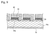
- the photoelectric conversion device comprises an electrically conductive layer 10, a photosensitive layer 20 composed of semiconductor fine particles 21 sensitized by a dye 22 and an electrolyte 23 penetrated into voids among the particles, a charge transfer layer 30, and a counter electrically conductive layer 40 laminated in this order, as shown in Fig. 1.
- the electrolyte 23 is preferably composed of the same materials as the components used in the charge transfer layer 30.
- the electrically conductive layer 10 and/or the counter electrically conductive layer 40 may be disposed a substrate 50 to improve the strength of the photoelectric conversion device.
- a layer composed of the electrically conductive layer 10 and the substrate 50 disposed thereon if necessary is referred to as "a conductive support", and a layer composed of the counter electrically conductive layer 40 and the substrate 50 disposed thereon if necessary is referred to as a "counter electrode”.
- a photo-electrochemical cell of the present invention is constituted by connecting the device to an outer circuit.
- the electrically conductive layer 10, the counter electrically conductive layer 40 and the substrate 50 shown in Fig. 1 may be a transparent electrically conductive layer 10a, a transparent counter electrically conductive layer 40a and a transparent substrate 50a, respectively.
- a light injected to the photosensitive layer 20 excites the dye 22, etc., excited high energy electrons therein are transported to a conduction band of the semiconductor fine particles 21, and they are diffused to reach to the electrically conductive layer 10.
- the dye 22 is in oxidized form.
- electrons in the electrically conductive layer 10 are returned to the oxidized dye through the counter electrically conductive layer 40 and the charge transfer layer 30 while working in the outer circuit, so that the dye 22 is regenerated.
- the photosensitive layer 20 acts as a negative electrode.
- each layer such as a boundary between the electrically conductive layer 10 and the photosensitive layer 20, a boundary between the photosensitive layer 20 and the charge transfer layer 30, a boundary between the charge transfer layer 30 and the counter electrically conductive layer 40, etc., components of each layer may be diffused and mixed.
- a boundary between the electrically conductive layer 10 and the photosensitive layer 20 and the photosensitive layer 20 and the charge transfer layer 30, a boundary between the charge transfer layer 30 and the counter electrically conductive layer 40, etc. components of each layer may be diffused and mixed.
- the conductive support is composed of: (1) a single layer of the electrically conductive layer; or (2) two layers of the electrically conductive layer and the substrate.
- the substrate is not necessary in the case where the electrically conductive layer has a high strength and can sufficiently seal the photoelectric conversion device.
- the electrically conductive layer is preferably made of a material having a sufficient strength and an electrical conductivity such as a metal, etc.
- the substrate having the electrically conductive layer comprising an electrically conductive agent at the photosensitive layer side.
- the electrically conductive agent include: metals such as platinum, gold, silver, copper, aluminum, rhodium and indium; carbon; and electrically conductive metal oxides such as indium-tin composite oxides and tin oxides doped with fluorine; etc.
- the thickness of the electrically conductive layer is preferably 0.02 to 10 ⁇ m.
- the surface resistance of the conductive support is preferably as low as possible.
- the surface resistance is preferably 100 ⁇ /square or less, more preferably 40 ⁇ /square or less.
- the lowest limit thereof is generally approximately 0.1 ⁇ /square, not limited in particular.
- the conductive support is substantially transparent.
- substantially transparent means the support has a light-transmittance of 10 % or more.
- the light-transmittance is preferably 50 % or more, particularly preferably 70 % or more.
- the transparent conductive support is preferably constituted by forming the transparent electrically conductive layer of an electrically conductive metal oxide on the transparent substrate of such material as a glass and a plastic by coating or vapor deposition.
- a transparent electrically conductive substrate made of a low-cost soda-lime float glass, on which the electrically conductive layer composed of a tin oxide doped with fluorine is deposited.
- a transparent polymer film disposed the electrically conductive layer thereon is preferably used as the transparent conductive support.
- the transparent polymer film examples include tetracetylcellulose (TAC), polyethylene terephthalate (PET), polyethylene naphthalate (PEN), syndiotactic polystyrene (SPS), polyphenylenesulfide (PPS), polycarbonate (PC), polyarylate (PAr), polysulfone (PSF), polyestersulfone (PES), polyetherimide (PEI), cyclic polyolefin, brominated phenoxy, etc.
- TAC tetracetylcellulose
- PET polyethylene terephthalate
- PEN polyethylene naphthalate
- SPS syndiotactic polystyrene
- PPS polyphenylenesulfide
- PC polycarbonate
- PAr polyarylate
- PSF polysulfone
- PET polyestersulfone
- PEI polyetherimide
- cyclic polyolefin brominated phenoxy, etc.
- a metal lead is used to reduce a resistance of the transparent conductive support.
- Material for the metal lead is preferably aluminum, copper, silver, gold, platinum, nickel, etc., particularly preferably aluminum or silver.
- the metal lead disposed the transparent electrically conductive layer of a tin oxide doped with fluorine, an ITO film, etc. thereon is preferably applied on the transparent substrate by a vapor deposition method, a sputtering method, or the like. It is also preferable that after forming the transparent electrically conductive layer on the transparent substrate, the metal lead is applied thereon.
- the reduction in quantity of incident light owing to the metal lead is suppressed to preferably 10 % or less, more preferably 1 to 5 %.
- the photosensitive layer preferably comprises semiconductor fine particles sensitized by a dye.
- the semiconductor fine particles act as a so-called "photosensitive substance" to absorb a light, thereby conducting a charge separation and generating electrons and positive holes.
- the dye-sensitized semiconductor fine particles the light-absorption and the generation of electrons and positive holes are primarily caused in the dye, the semiconductor fine particles receive and then convey the electrons.
- Used as the semiconductor fine particles may be: simple semiconductors such as silicone and germanium; III-V series compound semiconductors; metal chalcogenides such as oxides, sulfides and selenides; compounds with a perovskite structure such as strontium titanate, calcium titanate, sodium titanate, barium titanate and potassium niobate; etc.
- the semiconductor fine particles are preferably metal chalcogenide fine particles.
- metal chalcogenide examples include: oxides of titanium, tin, zinc, iron, tungsten, zirconium, hafnium, strontium, indium, cerium, yttrium, lanthanum, vanadium, niobium or tantalum; sulfides of cadmium, zinc, lead, silver, antimony or bismuth; selenides of cadmium or lead; and cadmium telluride; etc.
- other compound semiconductors include: phosphides of zinc, gallium, indium and cadmium; selenides of gallium-arsenic or copper-indium; and copper-indium sulfide; etc.
- the semiconductor used in the present invention include Si, TiO 2 , SnO 2 , Fe 2 O 3 , WO 3 , ZnO, Nb 2 O 5 , CdS, ZnS, PbS, Bi 2 S 3 , CdSe, CdTe, GaP, InP, GaAs, CuInS 2 and CuInSe 2 .
- the semiconductor may have a single crystal or poly crystal structure.
- the single crystal semiconductor is preferred from a viewpoint of a conversion efficiency, while the poly crystal semiconductor is preferred from viewpoints of a production cost, security of raw materials, an energy-payback time, etc.
- the particle size of the semiconductor fine particles is generally in the nm to ⁇ m level.
- the mean size of primary particles which is obtained from a diameter of a circle equivalent to a projected area, is preferably 5 to 200 nm, more preferably 8 to 100 nm.
- the mean size of the secondary semiconductor fine particles in dispersion is preferably 0.01 to 100 ⁇ m.
- the average particle size of the smaller particles is preferably 5 nm or less.
- the semiconductor fine particles having a large particle size e.g. approximately 300 nm, may be added to the mixture composing the semiconductor layer.
- Preferred as a method for producing the semiconductor fine particles are: sol-gel methods described in Sumio Sakka, “Science of a sol-gel method”, Agune Shofusha (1998), Technical information Association, “Thin film-coating technology by a sol-gel method” (1995), etc.; and gel-sol methods described in Tadao Sugimoto, “Synthesis of mono-dispersion particles and control of their size and form by a novel gel-sol method", and MATERIA, Vol. 35, No. 9, pp. 1012 to 1018 (1996).
- the method developed by Degussa Company which comprises preparing oxides by subjecting chlorides to a high temperature hydrolysis in an oxyhydrogen salt is also preferred.
- any of the above-described sol-gel methods, gel-sol methods and high temperature hydrolysis method is preferably used, and further a sulfuric acid method and a chlorine method described in Manabu Seino, "Titanium oxide - properties and applied technique", Gihodo Shuppan, (1997) may be used. Also preferred are sol-gel methods described in Christophe J. Barb'e, et al, Journal of American Ceramic Society, Vol. 80, No. 12, pp. 3157 to 3171 (1997) and Burnside, et al, Chemistry of Materials, Vol. 10, No. 9, pp. 2419 to 2425.
- the semiconductor fine particles may be coated on the conductive support by a method where a dispersion solution or a colloid solution containing the particles is applied on the electrically conductive layer, the above-mentioned sol-gel method, etc.
- a wet-type film production method is relatively advantageous for the mass production of the photoelectric conversion device, improvement of properties of semiconductor fine particle solution and adaptability of the conductive support, etc.
- a coating method and a printing method are typical examples.
- the sol-gel method mentioned above may be used as a method for preparing the dispersion solution containing the semiconductor fine particles. Further, the dispersion solution may be prepared by crushing the semiconductor in a mortar, dispersing the semiconductor while grinding in a mill, or precipitating the semiconductor fine particles in a solvent when the semiconductor is synthesized.
- dispersing solvent water or organic solvents such as methanol, ethanol, isopropyl alcohol, dichloromethane, acetone, acetonitrile, ethyl acetate, etc. may be used.
- a polymer, a surfactant, an acid, a chelating agent, etc. may be used as a dispersing agent, if necessary.
- Preferred coating methods are: a roller method and a dip method as an application series; an air-knife method and a blade method as a metering series; etc. Further, preferable as a method where an application and metering can be performed at the same time are a wire-bar method disclosed in JP-B-58-4589, a slide-hopper method described in United States Patent Nos. 2,681,294, 2,761,419, 2,761,791, etc., an extrusion method, a curtain method, etc. Furthermore, as for a wide use, a spin method and a spray method are preferred.
- a wet-type printing method three major printing methods comprising a relief printing, an offset printing and a gravure printing, and an intaglio printing, a gum-printing, a screen printing, etc. are preferred.
- a preferable film-production method may be selected from these methods in accordance with viscosity of the solution and a wet thickness.
- the viscosity of the dispersion solution material ly depends on the kind and dispersion property of the semiconductor fine particles, the kind of a solvent and additives such as a surfactant and a binder.
- a high viscosity solution e.g. 0.01 to 500 Poise
- an extrusion method, a cast method, a screen-printing method, etc. are preferably used.
- a low viscosity solution e.g. 0.1 Poise or less
- a slide-hopper method, a wire-bar method and a spin method are preferably used to form a uniform film.
- An extrusion method may be used for the low viscosity solution if it is coated to some extent.
- a wet-type film-production method may be properly selected in accordance with the viscosity of the coating solution, the coating amount, the support, a coating speed and so on.
- the layer of the semiconductor fine particles is not limited to a single layer.
- the dispersion solutions each comprising the semiconductor fine particles having a different particle size may be subjected to a multi-layer coating.
- coating solutions each containing different kinds of semiconductor fine particles, binder, or additives may be subjected to a multi-layer coating.
- a multi-layer coating is also effective when a film-thickness is insufficient by coating once. Suitable for the multi-layer coating are an extrusion method and a slide-hopper method.
- multi-layers may be coated at the same time, or alternatively they may be coated one over the other from several times to ten-several times. In the latter case, a screen method is also preferably used.
- a preferable thickness of the semiconductor fine particle layer is 0.1 to 100 ⁇ m.
- the thickness thereof is preferably 1 to 30 ⁇ m, more preferably 2 to 25 ⁇ m.
- a coating amount of the semiconductor fine particles per 1 m 2 of the support is preferably 0.5 to 400 g, more preferably 5 to 100 g.
- the particles are preferably subjected to a heat treatment to electronically contact them with each other, and to increase a coating strength and an adherence thereof with the support.
- a heating temperature is preferably 40 °C or more but less than 700 °C, more preferably 100 to 600 °C.
- a heating time is approximately 10 minutes to 10 hours. It is not preferred that a support having a low melting point or softening point such as a polymer film is subjected to a high temperature treatment because such a support tends to be deteriorated thereby.
- the heat treatment is preferably carried out at a temperature as low as possible also from a viewpoint of cost. The practice at such a low temperature is realized by a combination use with the above-described small semiconductor fine particles having a size of 5 nm or less, a heat treatment in the presence of a mineral acid, etc.
- a chemical metal-plating using an titanium tetrachloride aqueous solution, etc. or an electrochemical metal-plating using an titanium trichloride aqueous solution may be carried out to increase a surface area of the semiconductor fine particles, or to enhance a purity in the vicinity of the particles, thereby improving an efficiency of electron injection into the particles from the dye.
- the semiconductor fine particles have a large surface area, so that they can adsorb lots of dyes. Therefore, the surface area in the state that the semiconductor fine particle layer have been coated on the support is preferably 10 times or more, more preferably 100 times or more of the projected area. The highest limit, even though it is not limited in particular, is generally a level of 1000 times.
- the dye used for the photosensitive layer in the present invention is preferably a metal complex dye, a phthalocyanine dye and/or a methine dye, more preferably a metal complex dye and/or a methine dye.
- Two or more kinds of dyes may be used as a mixture to obtain a large photoelectric conversion wavelength region and a high photoelectric conversion efficiency.
- the dye and its mixing ratio may be selected in accordance with the wavelength region and the strength distribution of the light source.
- the dye preferably has an appropriate interlocking group for interacting with the surface of the semiconductor fine particles.
- Preferred interlocking groups include -COOH, -OH, -SO 3 H, a cyano group, -P(O)(OH) 2 , -OP(O)(OH) 2 , and chelating groups with ⁇ -conductivity such as oxime, dioxime, hydroxyquinoline, salicylate and ⁇ -ketoenolate groups.
- particularly preferred are -COOH, -P(O)(OH) 2 and -OP(O)(OH) 2 .
- the interlocking group may form a salt with an alkali metal, etc. or an intramolecular salt. If the methine chain of the polymethine dye has an acidic group as in the case where the methine chain forms a squarylium ring or a croconium ring, it may act as the interlocking group.
- the preferred dyes used for the photosensitive layer will be specifically described below.
- the metal complex dye used in the present invention is preferably ruthenium complex.
- the ruthenium complex dyes described in United States Patent Nos. 4,927,721, 4,684,537, 5,084,365, 5,350,644, 5,463,057, 5,525,440, Japanese Patent Laid-Open No. 7-249790, WO 98/50393, etc. may be used in the present invention.
- the ruthenium complex dye is preferably represented by the following formula (I): (A 1 ) p Ru(B-a)(B-b)(B-c) wherein A 1 represents a ligand selected from the group consisting of Cl, SCN, H 2 O, Br, I, CN, NCO and SeCN; p represents an integer of 0 to 2, preferably 2; and B-a, B-b, and B-c independently represent an organic ligand selected from the compounds represented by the following formulae B-1 to B-8.
- a 1 represents a ligand selected from the group consisting of Cl, SCN, H 2 O, Br, I, CN, NCO and SeCN
- p represents an integer of 0 to 2, preferably 2
- B-a, B-b, and B-c independently represent an organic ligand selected from the compounds represented by the following formulae B-1 to B-8.
- R 11 represents a substituent. Specific examples thereof include: a halogen atom; a substituted or unsubstituted alkyl group having 1 to 12 carbon atom; a substituted or unsubstituted aralkyl group having 7 to 12 carbon atoms; a substituted or unsubstituted aryl group having 6 to 12 carbon atoms; an acidic group that may form a salt such as a carboxyl group and a phosphono group; etc.
- the alkyl group and the alkyl moiety of the aralkyl group may be straight or branched, and the aryl group and the aryl moiety of the aralkyl group may have a monocyclic structure or a polycyclic structure such as a condensed ring and a ring assemblage.
- B-a, B-b and B-c may be the same or different ligands.
- the methine dyes preferably used in the present invention include those represented by any of the following general formulae (II), (III), (IV) and (V).
- R 21 and R 25 independently represent a hydrogen atom, an alkyl group, an aryl group or a heterocyclic group;
- R 22 to R 24 independently represent a hydrogen atom or a substituent;
- R 21 to R 25 may be bonded together to form a ring;
- L 11 and L 12 independently represent a nitrogen atom, an oxygen atom, a sulfur atom, a selenium atom or a tellurium atom;
- n1 and n3 independently represent an integer of 0 to 2; and
- n2 represents an integer of 1 to 6.
- This dye may have a counter ion in agreement with the charge quantity of the whole molecule.
- the above-mentioned alkyl group, aryl group and heterocyclic group may have a substituent.
- the alkyl group may be a straight or branched, and the aryl group and the heterocyclic group may have a monocyclic structure or a polycyclic structure such as a condensed ring and a ring assemblage.
- the ring formed by R 21 to R 25 may have a substituent, and may be a monocyclic ring or a condensed ring.
- Z a represents a non-metal atomic group forming a nitrogen-containing heterocyclic group
- R 31 represents an alkyl group or an aryl group.
- Q a represents a methine group or a polymethine group necessary to act as a polymethine dye.
- the dye may form an oligomer or a polymer through Q a .
- X 3 represents a counter ion, and n4 indicating a number thereof represents an integer of 0 to 10.
- the nitrogen-containing heterocyclic ring formed by Z a may have a substituent, and may be a monocyclic ring or a condensed ring.
- the alkyl or aryl group represented by R 31 may have a substituent, the alkyl group may be a straight or branched, and the aryl group may have a monocyclic structure or a polycyclic structure such as a condensed ring and a ring assemblage.
- dyes represented by the general formula (III) more preferred are those represented by any of the following general formulae (III-a) to (III-d): wherein R 41 to R 45 , R 51 to R 54 , R 61 to R 63 and R 71 to R 73 independently represent a hydrogen atom, an alkyl group, an aryl group or a heterocyclic group; L 21 , L 22 , L 31 , L 32 , L 41 to L 45 and L 51 to L 56 independently represent an oxygen atom, a sulfur atom, a selenium atom, a tellurium atom, -CRR'- or -NR- (in which R and R' independently represent a hydrogen atom, an alkyl group, an aryl group or a heterocyclic group, and may be the same or different); L 33 represents O - , S - , Se - , Te - or N - R (in which R represents a hydrogen atom, an alkyl group, an aryl group or a
- the dyes represented by any one of the general formulae (III-a) to (III-d) may have a counter ion in agreement with the charge of the molecule.
- the alkyl group, the aryl group and the heterocyclic group mentioned above may have a substituent, the alkyl group may be straight or branched, and the aryl group and the heterocyclic group may have a monocyclic structure or a polycyclic structure such as a condensed ring and a ring assemblage.
- polymethine dyes represented by the general formula (III) are described in detail in M. Okawara, T. Kitao, T. Hirashima and M. Matsuoka, Organic Colorants, Elsevier, etc.
- Q b represents an atomic group forming a 5-or 6-membered nitrogen-containing heterocycle
- Z b represents an atomic group forming a 3- to 9-membered ring
- L 61 to L 65 independently represent a substituted or unsubstituted methine group.
- n8 is an integer of 0 to 4, preferably 0 to 3, and n9 is 0 or 1.
- R 81 represents a substituent
- X 4 represents a counter ion contained if necessary to neutralize charge of the dye.
- the nitrogen-containing heterocycle formed by Q b may be a condensed ring, and may have a substituent.
- the heterocycle include a benzothiazole ring, a benzoxazole ring, a benzoselenazole ring, a benzotellurazole ring, a 2-quinoline ring, a 4-quinoline ring, a benzoimidazole ring, a thiazoline ring, an indolenine ring, an oxadiazole ring, a thiazole ring and an imidazole ring.
- a benzothiazole ring a benzoxazole ring, a benzoimidazole ring, a benzoselenazole ring, a 2-quinoline ring, a 4-quinoline ring and an indolenine ring are more preferred, a benzothiazole ring, a benzoxazole ring, a 2-quinoline ring, a 4-quinoline ring and an indolenine ring are particularly preferred.
- the substituent on Q b include: a carboxyl group; a phosphonyl group; a sulfonyl group; halogen atoms such as F, Cl, Br and I; a cyano group; an alkoxy group such as a methoxy group, an ethoxy group and a methoxyethoxy group; an aryloxy group such as a phenoxy group; an alkyl group such as a methyl group, an ethyl group, a cyclopropyl group, a cyclohexyl group, a trifluoromethyl group, a methoxyethyl group, an allyl group and a benzyl group; an alkylthio group such as a methylthio group and an ethylthio group; an alkenyl group such as a vinyl group and a 1-propenyl group; an aryl group such as a phenyl group, a chlorophen
- Z b is preferably composed of atoms selected from the group consisting of carbon, oxygen, nitrogen, sulfur and hydrogen atoms.
- the ring formed by Z b is preferably a ring with a 4 to 6 carbon skeleton, more preferably such that represented by any one of the following (a) to (e), the most preferably such that represented by (a).
- Examples of the substituent on L 61 to L 65 include: a substituted or unsubstituted alkyl group having preferably 1 to 12, more preferably 1 to 7 carbon atom, such as a methyl group, an ethyl group, a propyl group, an isopropyl group, a cyclopropyl group, a butyl group, a 2-carboxyethyl group and a benzyl group; a substituted or unsubstituted aryl group preferably having 6, 8 or 10 carbon atoms, more preferably 6 or 8 carbon atoms, such as a phenyl group, a tolyl group, a chlorophenyl group and an o -carboxyphenyl group; a heterocyclic group such as a pyridyl group, a thienyl group, a furanyl group and a barbituric acid group; a halogen atom such as a chlorine atom and a bromine atom
- the substituents may be bonded together to form a cyclopentene ring, a cyclohexene ring, a squalilium ring, etc. Further, the substituents may combine an auxochrome to form a ring.
- the substituent represented by R 81 is preferably an aliphatic group that may have a substituent or an aromatic group that may have a substituent.
- the aliphatic group has preferably 1 to 10, more preferably 1 to 6 carbon atom.
- the aromatic group has preferably 1 to 16 carbon atom, more preferably 5 or 6 carbon atoms.
- Examples of the unsubstituted aliphatic group and aromatic group include a methyl group, an ethyl group, a n -propyl group, a n -butyl group, a phenyl group and a naphthyl group.
- Typical positive counter ions are inorganic or organic ammonium ions such as a tetraalkyl ammonium ion, a pyridinium ion, etc. and alkali metal ions.
- negative counter ions may be inorganic or organic, and examples thereof include: a halide ion such as a fluoride ion, a chloride ion, a bromide ion and an iodide ion; a substituted aryl sulfonate ion such as a p -toluene sulfonate ion and a p -chlorobenzene sulfonate ion; an aryl disulfonate ion such as a 1,3-benzene disulfonate ion, a 1,5-naphthalene disulfonate ion and a 2,6-naphthalene disulfonate ion; an alkyl sulfate ion such as a methyl sulfate ion; a sulfate ion; a thiocyanate ion; a perchlorate ion
- ionic polymers or other dyes having an opposite charge to the dye may be also used as a charge-balancing counter ion.
- metal complex such as bisbenzene-1,2-dithiolato nickel (III) can be also used in the present invention.
- Q c represents an at least tetravalent aromatic group
- L 71 and L 72 independently represent a sulfur atom, a selenium atom or -CRR'- (R and R' independently represent a hydrogen atom or an alkyl group).
- L 71 and L 72 are preferably a sulfur atom or -CRR'-, more preferably -CRR'-, respectively.
- R 91 and R 92 independently represent an alkyl group or an aromatic group
- Y 51 and Y 52 independently represent a non-metal atomic group necessary to act as a polymethine dye.
- X 5 represents a counter ion.
- Q c examples include at least tetravalent aromatic groups derived from: an aromatic hydrocarbon such as benzene, naphthalene, anthracene and phenanthrene; or an aromatic heterocyclic ring such as anthraquinone, carbazole, pyridine, quinoline, thiophene, furan, xanthene and thianthrene.
- the aromatic group may have a substituent.
- Q c is derived from preferably aromatic hydrocarbon, more preferably benzene or naphthalene.
- Various kinds of methine dyes can be formed by Y 51 and Y 52 . It is preferably that Y 51 and Y 52 form a cyanine dye, a merocyanine dye, a rhodacyanine dye, a trinuclear merocyanine dye, an allopolar dye, a hemicyanine dye or a styryl dye.
- the cyanine dyes include such that having substituents on the methine chain forming a squalium ring, a croconium ring, etc. Details of the dyes represented by the general formula (V) are described in: F. M.
- the dye represented by the general formula (V) has a squalilium ring on preferably at least one methine chain, more preferably the both methine chains.
- R 91 and R 92 are independently an alkyl group or an aromatic group, and may have a substituent.
- the aliphatic group has preferably 1 to 10 carbon atom, more preferably 1 to 6 carbon atom.
- the aromatic group has preferably 5 to 16 carbon atoms, more preferably 5 or 6 carbon atoms. Examples of the unsubstituted aliphatic group and aromatic group include a methyl group, an ethyl group, a n -propyl group, a n -butyl group, a phenyl group and a naphthyl group.
- R 91 , R 92 , Y 51 and Y 52 has an acidic group.
- the acidic group is a group with a dissociative proton, such as a carboxylic acid group, a phosphonic acid group, a sulfonic acid group, a boric acid group, etc. Among them, preferred is a carboxylic acid group.
- the dissociative proton of the acidic group may be dissociated.
- the dyes represented by the formulae (II) and (III) can be synthesized by the methods described in: F. M. Harmer, "Heterocyclic Compounds -Cyanine Dyes and Related Compounds", John Wiley & Sons, New York, London (1964); D. M. Sturmer, "Heterocyclic Compounds -Special Topics in Heterocyclic Chemistry", chapter 18, section 14, pp. 482 to 515, John Wiley & Sons, New York, London (1977); “Rodd's Chemistry of Carbon Compounds", 2nd. Ed., vol. IV, part B, chapter 15, pp. 369 to 422, Elsevier Science Publishing Company Inc., New York (1977); British Patent No.
- the dyes represented by the formula (IV) can be synthesized based on the methods described in Dyes and Pigments, vol. 21, pp. 227 to 234, etc.
- the dyes represented by the formula (V) can be synthesized based on: Ukrainskii Khimicheskii Zhurnal, vol. 40, No. 3, pp. 253 to 258; Dyes and Pigments, vol. 21, pp. 227 to 234; and references therein.
- the dye may be adsorbed to the semiconductor fine particles by soaking the conductive support having the well-dried semiconductor fine particle layer in a dye solution, or by coating the dye solution to the semiconductor fine particle layer.
- a soaking method, a dipping method, a roller method, an air-knife method, etc. may be used.
- the dye may be adsorbed at a room temperature or while refluxing as described in Japanese Patent Laid-Open No. 7-249790.
- a coating method of the latter a wire-bar method, a slide-hopper method, an extrusion method, a curtain method, a spin method, a spray method, etc. may be used.
- a printing method a relief printing, an offset printing, a gravure printing, a screen-printing, etc. may be used.
- a solvent for the dye solution may be properly selected in accordance with the solubility of the dye.
- alcohols such as methanol, ethanol, t -butanol, benzyl alcohol, etc.
- nitriles such as acetonitrile, propionitrile, 3-methoxypropionitrile, etc.
- nitromethane halogenated hydrocarbons such as dichloromethane, dichloroethane, chloroform, chlorobenzene, etc.
- ethers such as diethylether, tetrahydrofuran, etc.
- dimethylsulfoxide amides such as N,N -dimethylformamide, N,N -dimethylacetamide, etc.
- N -methylpyrrolidone 1,3-dimethylimidazolidinone; 3-methyloxazolidinone
- esters such as ethyl acetate, butyl acetate, etc.
- carbonates such as diethyl carbon
- an extrusion method and various kinds of printing methods are suitable for a high viscosity solution (e.g. 0.01 to 500 Poise), and a slide-hopper method, a wire bar method and a spin method are suitable for a low viscosity solution (e.g. 0.1 Poise or less) to form a uniform film.
- a high viscosity solution e.g. 0.01 to 500 Poise
- a slide-hopper method e.g. 0.01 to 500 Poise
- a wire bar method and a spin method are suitable for a low viscosity solution (e.g. 0.1 Poise or less) to form a uniform film.
- the dye adsorption method may be properly selected in accordance with the viscosity of the dye solution, the coating amount, the conductive support, the coating speed, etc. It is preferable that the dye-adsorbing time after coating is as short as possible from a viewpoint of mass production.
- the unadsorbed dyes are preferably removed by washing immediately after adsorption because they often cause disturbance of efficiency of the device.
- the washing is preferably carried out using a wet-type washing bath with a polar solvent such as acetonitrile, or an organic solvent such as an alcohol-based solvent.
- a heat treatment is preferably carried out before the adsorption. After the heat treatment, it is preferable that the dye is quickly adsorbed at 40 to 80 °C without cooling to a room temperature in order to prevent adsorption of water to the surface of the semiconductor fine particles.
- the total amount of the dye is preferably 0.01 to 100 mmol per the unit surface area (1 m 2 ) of the conductive support.
- the amount of the dye adsorbed to the semiconductor fine particles is preferably 0.01 to 1 mmol per 1 g of the semiconductor fine particles.
- Such an adsorption amount of the dye effects a sufficient sensitization to the semiconductors.
- the sensitization effect is not sufficient.
- the dye unadsorbed to the semiconductor fine particles floats to reduce sensitization effect.
- Two or more kinds of dyes may be mixed and used for the photoelectric conversion device to extend the conversion wavelength range and to increase a conversion efficiency.
- the dyes and their proportion are preferably selected in accordance with the wavelength region and the intensity distribution of a light source.
- a colorless compound may be co-adsorbed on the semiconductor fine particles together with the dye to weaken an interaction, such as association, between the dyes.
- Used as a hydrophobic compound for the co-adsorption may be a steroid compound having a carboxyl group such as chenodeoxycholic acid, etc.
- An UV-absorbing agent may be used together therewith.
- the surface of the semiconductor fine particles may be treated with amines after dye adsorption to accelerate to remove an excessive dye.
- amines include pyridine, 4- t -butylpyridine, polyvinylpyridine, etc.
- the amine may be used as it is, or as a solution with an organic solvent when it is liquid.
- the charge transfer layer replenishes electrons to the oxidized dye.
- the charge transfer layer comprises the electrolyte composition of the present invention mentioned above.
- a solid electrolyte and a hole-transporting material may be also used therefor.
- the charge transfer layer is preferably formed by applying the electrolyte composition to the photosensitive layer using a casting method, a coating method, a soaking method, a loading method, etc., and heating if necessary.
- the charge transfer layer may be formed by: preparing the uniform solution of the electrolyte composition comprising the molten salt, additives such as a coating quality-improving agent (a leveling agent, etc.), etc.; coating the solution by a spin coating method, a dip coating method, an air-knife coating method, a curtain coating method, a roller coating method, a wire-bar coating method, a gravure coating method, an extrusion coating method using a hopper described in United States Patent No. 2,681,294, a simultaneous multi-layer coating method described in United States Patent Nos. 2,761,418, 3,508,947 and 2,761,791; and heating if necessary.
- a coating quality-improving agent a leveling agent, etc.
- the heating temperature is properly selected in accordance with a heat-resistance of the dye, etc.
- the temperature is preferably 10 to 150 °C, more preferably 10 to 100 °C in general.
- the heating time, depending on the heating temperature, etc., may be approximately 5 minutes to 72 hours.
- the solution of the electrolyte composition is coated in an excess of the amount with which voids in the photosensitive layer are completely fulfilled. Therefore, the resulting electrolyte layer substantially exists from the surface of the electrically conductive layer 10 to the surface of the counter electrically conductive layer 40, as shown in Fig. 1.
- the electrolyte layer is defined as the charge transfer layer 30, the thickness thereof is preferably 0.001 to 200 ⁇ m, more preferably 0.1 to 100 ⁇ m, particularly preferably 0.1 to 50 ⁇ m.
- the charge transfer layer 30 has thickness of less than 0.001 ⁇ m, there is a fear that the semiconductor fine particles 21 in the photosensitive layer comes in contact with the counter electrically conductive layer 40.
- the total thickness of the photosensitive layer 20 and the charge transfer layer 30, which is substantially equal to the thickness of the electrolyte layer is preferably 0.1 to 300 ⁇ m, more preferably 1 to 130 ⁇ m, particularly preferably 2 to 75 ⁇ m.
- iodine, etc. may be introduced by: adding it to the above-mentioned solution of the electrolyte composition; or placing the support disposed the charge transfer layer thereon in a sealed vessel with iodine, etc., thereby diffusing it into the electrolyte; etc. Further, iodine may be introduced to the charge transfer layer by coating or vapor-depositing it on the counter electrode before constituting the photoelectric conversion device.
- the counter electrode acts as an anode of the cell.
- the counter electrode may be a single layer of a counter conductive layer of an electrically conductive material, or composed of the counter electrically conductive layer and a support, as is similar to the above-described conductive support.
- the conductive material for the counter electrically conductive layer include: metals such as platinum, gold, silver, copper, aluminum, rhodium and indium; carbon; and electrically conductive metal oxides such as indium-tin composite oxides and fluorine-doped tin oxides.
- the substrate for the counter electrode is preferably made of glass or plastic, and the electrically conductive layer is coated or vapor-deposited thereon.
- the thickness of the counter electrically conductive layer is not limited in particular, preferably 3 nm to 10 ⁇ m. In the case of the metal counter electrically conductive layer, the thickness thereof is preferably 5 ⁇ m or less, more preferably 5 nm to 3 ⁇ m.
- a light may be irradiated from any one or both side of the conductive support and the counter electrode. At least one of them must be substantially transparent to have light reached to the photosensitive layer. From a viewpoint of improving an electric generation efficiency, it is preferably that the conductive support is transparent and light is irradiated through it.
- the counter electrode preferably has a light-reflective property. Glass or plastic having vapor-deposited metal or electrically conductive oxides thereon, or a metal thin film can be preferably used as a material for such a counter electrode.
- the counter electrode may be disposed (i) on the charge transfer layer formed beforehand, or (ii) on the semiconductor fine particle layer through a spacer before forming the charge transfer layer.
- the counter electrode may be disposed by: directly coating, metal-plating, or vapor-depositing (PVD, CVD, etc.) the electrically conductive material on the charge transfer layer; or laminating the electrically conductive layer formed on the substrate on the charge transfer layer.
- the counter electrode is disposed on the semiconductor fine particle layer through the spacer, and the open ends therebetween is soaked in the solution of the electrolyte composition. The solution penetrates into the voids between the counter electrode and the semiconductor fine particle layer by capillarity or reduced pressure.
- the metal lead for reducing the resistance of the electrode particularly in the case of the transparent counter electrode.
- Preferable embodiments of the metal lead are the same as the case of the conductive support mentioned above.
- Functional layers such as a protective layer and a reflection-preventing layer may be disposed on one or both of the conductive support and the counter electrode each acting as the electrode.
- Such functional layers may be formed in a fashion of multi-layers by a simultaneous multi-layer coating method or a successive coating method.
- the simultaneous multi-layer coating method is preferred from a viewpoint of productivity.
- a slide-hopper method and an extrusion method are preferable from the viewpoint of the productivity and homogeneity of a coated film.
- the functional layers may be disposed by a method selected in accordance with the materials for the layer, such as a vapor-deposition method and a sticking method.
- An undercoating layer may be disposed between the conductive support and the photosensitive layer to prevent short-circuit of the device.
- the undercoating layer is preferably composed of a semiconductor thin film.
- Preferable materials therefor include TiO 2 , SnO 2 , Fe 2 O 3 , WO 3 , ZnO and Nb 2 O 5 . Among them, TiO 2 is more preferred.
- the undercoating layer may be disposed by a spray-pyrolysis method described in Electrochim. Acta, 40, 643 to 652 (1995).
- the thickness of the undercoating layer is preferably 5 to 1000 nm, more preferably 10 to 500 nm.
- the photoelectric conversion device may have various interior structures in accordance with an end of use. These structures are classified into two major forms, a structure allowing incidence of light from both faces, and a structure allowing it from only one face.
- Fig. 2 to 8 each illustrate examples of the interior structure of the photoelectric conversion device that can be preferably used in the present invention.
- a photosensitive layer 20 and a charge transfer layer 30 are disposed between a transparent electrically conductive layer 10a and a transparent counter electrically conductive layer 40a. This structure allows incidence of a light from both faces of the device.
- a transparent electrically conductive layer 10a As for the structure illustrated in Fig. 3, on a transparent substrate 50a partially having a metal lead 11 is disposed a transparent electrically conductive layer 10a, an undercoating layer 60, a photosensitive layer 20, a charge transfer layer 30 and a counter electrically conductive layer 40 are laminated in this order, and a substrate 50 is further placed thereon.
- This structure allows incidence of light from the electrically conductive layer side.
- a photosensitive layer 20 is disposed on a substrate 50 having an electrically conductive layer 10 thereon through an undercoating layer 60, a charge transfer layer 30 and a transparent counter electrically conductive layer 40a are disposed thereon, and further a transparent substrate 50a locally having a metal lead 11 is placed so that the metal lead 11 side orients inward.
- This structure allows incidence of light from the counter electrode side.
- a transparent electrically conductive layer 10a or a transparent counter electrically conductive layer 40a partially are formed on two transparent substrates 50a each having a metal lead 11 partially are formed a transparent electrically conductive layer 10a or a transparent counter electrically conductive layer 40a, respectively, and an undercoating layer 60, a photosensitive layer 20 and a charge transfer layer 30 placed between the conductive layers.
- This structure allows incidence of light from both faces of the photoelectric conversion device.
- a photosensitive layer 20 As for the structure illustrated in Fig. 6, on a transparent substrate 50a having a transparent electrically conductive layer 10a is disposed a photosensitive layer 20 through an undercoating layer 60, a charge transfer layer 30 and a counter electrically conductive layer 40 are formed thereon, and further a substrate 50 is placed thereon.
- This structure allows incidence of light from the electrically conductive layer side.
- a photosensitive layer 20 As for the structure illustrated in Fig. 7, on a substrate 50 having an electrically conductive layer 10 is disposed a photosensitive layer 20 through an undercoating layer 60, a charge transfer layer 30 and a transparent counter electrically conductive layer 40a are formed thereon, and further a transparent substrate 50a is placed thereon.
- This structure allows incidence of light from the counter electrode side.
- a transparent substrate 50a having a transparent electrically conductive layer 10a is disposed on a transparent substrate 50a having a transparent electrically conductive layer 10a through an undercoating layer 60, a charge transfer layer 30 and a transparent counter electrically conductive layer 40a are formed thereon, and further a transparent substrate 50a is placed thereon.
- This structure allows incidence of light from both faces of the photoelectric conversion device.
- the photo-electrochemical cell of the present invention comprises the above-described photoelectric conversion device designed to work in the outer circuit.
- the side face of the photo-electrochemical cell is preferably sealed with a polymer or an adhesive agent, etc. to prevent deterioration of the compositions thereof and volatility of the content in the cell.
- the outer circuit is connected to the conductive support and the counter electrode via a lead.
- Various known circuits may be used in the present invention.
- the interior structure of a cell may be essentially the same as the photoelectric conversion device mentioned above.
- Module structures of the solar cell comprising the photoelectric conversion device of the present invention will be explained below.
- the dye-sensitized solar cell of the present invention may have the same module structure as that of prior art solar cells.
- the solar cell module generally has a structure where cells are placed on a substrate of metal, ceramic, etc., they are covered with a packing resin, a protective glass, etc., and light is introduced from an opposite side of the substrate.
- the solar cell module may have a structure where the cells are placed on a substrate of a transparent material such as a tempered glass, and light is introduced from the transparent substrate side.
- a superstraight type module structure, a substrate type module structure, a potting type module structure, substrate-integrated type module structure used for an amorphous silicon solar cell, etc. are known as the solar cell module structure.
- the dye-sensitized solar cell of the present invention may have a module structure properly selected from the above structures in accordance with ends, environment at use.
- the super straight type module and the substrate type module generally have a structure where the cells are placed at a regular intervals between substrates, and connected by a metal lead, a flexible wirering, etc., and collector electrodes are placed at the outer marginal portion so that a generated electric power can be delivered to the outside.
- the substrate is subjected to a reflection-preventing treatment, and one or both side thereof is transparent.
- plastic material such as ethylene vinyl acetate (EVA) to protect the cell or to improve a collector efficiency.
- EVA ethylene vinyl acetate
- Such a plastic material is may be used in a form of a film or a packing resin.
- one of the substrate can be omitted by forming a surface protective layer of a transparent plastic film, or by hardening the above-described packing resin to give a protection function.
- the periphery of the substrates may be sandwiched and fixed by metallic flames, and the substrates and the flames may be sealed with a sealant in order to seal the interior of the cell and to secure rigidity of a module.
- flexible materials may be used for the cell, the substrate, the packing agent and the sealant to constructing the solar cell on a curved surface.
- the super straight type solar cell module may be manufactured by the following steps of: placing cells on a front substrate sent out from a substrate-supplying device together with lead lines for connecting a sealant to the cells and a sealant for back surface while carrying the front substrate by a belt conveyer, etc.; placing a back substrate or a back cover thereon; and setting flames at the outer edge portion.
- the substrate type solar cell may be manufactured by the following steps of: placing cells on a substrate sent out from a substrate-supplying device together with lead lines for connecting the cells and a sealant, etc. while carrying the substrate by a belt conveyer, etc.; placing a front cover thereon; and setting flames at the outer edge portion.
- Fig. 9 shows a structure of an embodiment of the substrate-integrated type solar cell produced by modularizing a photoelectric conversion device of the present invention.
- the solar cell shown in Fig. 9 has a structure where cells having a transparent electrically conductive layer 10a, a photosensitive layer 20 containing dye-adsorbed TiO 2 , a charge transfer layer 30 and a metal counter electrically conductive layer 40 are modularized on one surface of a transparent substrate 50a, and a reflection-preventing layer 70 is applied on the other surface of the substrate.
- a desired module structure can be obtained by patterning according to a semiconductor process technique such as selective metal plating, selective etching, CVD, PVD, etc., or a mechanical method such as laser scribing, plasma CVM, polishing, etc. so that the transparent electrically conductive layers, the photosensitive layers, the charge transfer layers and the counter electrode etc. are three-dimensionally arranged at a regular interval on the substrate.
- a semiconductor process technique such as selective metal plating, selective etching, CVD, PVD, etc.
- a mechanical method such as laser scribing, plasma CVM, polishing, etc.
- various materials such as a liquid EVA (ethylene vinyl acetate), an EVA film, a mixture of fluorinated vinylidene copolymer and an acrylic resin, etc. may be used in accordance with objects such as application of weather-resistance or electric insulation, improvement in light-condensing efficiency, protection of a cell (improvement in impact resistance), etc.
- the outer edge of the module and the frame surrounding the fringe are preferably sealed with the sealant having high weather-resistance and moisture permeability.
- the strength and light transmittance of the sealed cell can be enhanced by adding a transparent filter into the sealant.
- a method suited to a property of the sealant is preferably used.
- Various methods therefor may be used such as roll pressurization followed by thermal adherence, vacuum pressurization followed by thermal adherence, etc. for the film sealant, and roll coat, bar coat, spray coat, screen printing, etc. for the liquid or paste sealant.
- a flexible material such as PET and PEN is used for a substrate, because after constructing the cells on a roll-like support, the sealing layer can be successively laminated according to the above-described methods to obtain a high productivity.
- the light-taking surface of the substrate, generally a tempered glass substrate, of the module may be subjected to a reflection-preventing treatment.
- the reflection-preventing treatment may comprise laminating a reflection-preventing film, coating a reflection-preventing layer, etc.
- the surface of the cell may be grooved or textured, thereby enhancing efficiency of utilizing incident light.
- the light reflectance may be increased by vapor-depositing or metal-plating the substrate with Ag, Al, etc. after a mirror plane-polishing, applying a layer comprising an Al-Mg alloy, an Al-Ti alloy, etc. as reflective layer at the lowest layer in the solar cell, making the lowest layer to a texture structure by annealing.
- the cells are generally connected each other by a wire bonding method or using an electrically conductive flexible sheet.
- the cells may be connected by methods such as electrically connecting while fixing the cells by an electrically conductive adhesives, adhesive tapes, etc., and pattern-coating an electrically conductive hot melt at an intended position.
- a solar cell comprising a flexible support made of a polymer film, etc. may be manufactured by a method comprising the steps: forming cells in the same manner as described above while sending out a roll-like support; cutting it to an intended size; and sealing the marginal portion thereof with a flexible, moisture permeable material.
- the solar cell may have a module structure called "SCAF" described in Solar Energy Materials and Solar Cells, 48, p 383 to 391. Further, the solar cell comprising the flexible support may be used while adhered and fixed to a curved glass, etc.
- the solar cells comprising the photoelectric conversion device of the present invention may have various kinds of forms and functions in accordance with ends and environment of use.
- the compounds represented by the general formula (1) were synthesized, using the compounds a to d shown below.
- the structure of product was identified by 1 H-NMR. Water-content of the product was measured by Karl Fisher method, and the viscosity thereof was measured by the B-type viscometer manufactured by TOKIMEC INC.
- a 200 ml inner volume of a stainless steel vessel coated with Teflon inside was charged with 15 g of titanium dioxide fine particles "Degussa P-25" manufactured by Nippon Aerosil K.K., 45 g of water, 1 g of dispersant "Triton X-100" manufactured by Aldrich, and 30 g of zirconia beads having a diameter of 0.5 mm manufactured by Nikkato K.K. These contents were subjected to a dispersion treatment for 2 hours at 1500 rpm by means of a sand-grinder mill manufactured by Imex K.K. The zirconia beads were removed by filtration to obtain the titanium dioxide dispersion. The average particle diameter of the titanium dioxide particles in the dispersion was 2.5 ⁇ m. Herein, the particle diameter was measured by Master Sizer manufactured by MALVERN.
- the above dispersion was coated on an electrically conductive surface of a conductive glass having a fluorine-doped tin oxide layer by a glass bar.
- a conductive glass having a fluorine-doped tin oxide layer by a glass bar.
- Used as the conductive glass was 20 mm ⁇ 20 mm of "TCO Glass-U” manufactured by Asahi Glass K.K. with a surface resistance of approximately 30 ⁇ /square.
- a coating amount of the semiconductor fine particles was 20 g/m 2 .
- the coated glasses were air-dried for a day at a room temperature after peeling the adhesive tapes. Then, the glasses were placed in an electric furnace "muffle furnace FP-32" manufactured by Yamato Science K.K., followed by calcinating at 450 °C for 30 minutes to obtain TiO 2 electrodes.
- the electrodes were taken out of the furnace and cooled, they were immersed in ethanol solution comprising the dye shown in Table 1 for 3 hours to adsorbing the dye, respectively.
- the concentration of the dye in the ethanol solution was 3 ⁇ 10 -4 mol/l.
- the dye-adsorbed TiO 2 electrodes were further immersed in 4- t -butylpyridine for 15 minutes, then washed with ethanol and air-dried.
- the thickness of thus-obtained photosensitive layer was shown in Table 1, and an adsorbing amount of the dye was appropriately selected in a range of 0.1 to 10 mmol/m 2 according to the dye.
- the 20 mm ⁇ 20 mm in size of dye-sensitized TiO 2 electrode glass substrate prepared as described above was put on a platinum-vapor deposited glass having the same size.
- an electrolyte composition was permeated into a crevice between the glasses through capillarity to be introduced into the TiO 2 electrode, thereby obtaining a photo-electrochemical cell.
- the photo-electrochemical cell similar to that shown in Fig.
- the conductive support of the electrically conductive glass comprising the transparent substrate 50a of glass and the electrically conductive layer 10a disposed thereon; the photosensitive layer 20 of the dye-sensitized TiO 2 ; the charge transfer layer 30; the counter electrically conductive layer 40 of platinum; and the transparent substrate 50a of glass were laminated in this order, and sealed with an epoxy-based sealant.
- the photo-electrochemical cell was produced by the method comprising the steps of: warming the electrolyte composition to 50 °C; applying it on the TiO 2 electrode; sufficiently permeating the electrolyte composition into the electrode and removing air in the electrode under reduced pressure; and putting a platinum-deposited counter electrode glass thereon.
- the compound represented by the general formula (1) used for the electrolyte composition has a substituent, a conjugate acid of a compound obtained by adding a hydrogen atom thereto exhibiting a pKa value of 3 to 15.
- a substituent is: a pyridyl group (the pKa value: 5) in the case of 1-a to 1-f and 15-c; an ⁇ -picolyl group (the pKa value: 6) in the case of 2-b, 2-c, 3-d, 3-e, 4-c to 4-f and 5-c; a 2-methylimidazolyl group (the pKa value: 8) in the case of 7-c; and an imidazolyl group (the pKa value: 7) in the case of 13-c.
- the structure of compounds Y-1 to Y-8 used in the EXAMPLES and COMPARATIVE EXAMPLES will be illustrated below.
- a simulated sunlight was irradiated to the photo-electrochemical cells of EXAMPLES and COMPARATIVE EXAMPLES at 55 °C, and the generated electricity was measured by the current-voltage tester "Keithley SMU238", to obtain open circuit voltage (Voc), short-circuit current density (Jsc), fill factor (FF), photoelectric conversion efficiency ( ⁇ ), and decrease (%) of photoelectric conversion efficiency after storage in the dark for 80 hours with respect to each of the cells.
- the results are shown in Table 2.
- the simulated sunlight was obtained by passing the light of a 500 W xenone lamp manufactured by Ushio K.K. through an "AM 1.5 filter” manufactured by Oriel Co. and a sharp cut filter "Kenko L-42".
- the electrolyte composition preferably comprises 10 weight % or less of solvent, more preferably comprises no solvent.
- the cells comprising the electrolyte composition with no solvent
- the cells of COMPARATIVE EXAMPLES 6 to 10 using only conventional imidazolium salts and COMPARATIVE EXAMPLES 11 to 15 using the salts and the basic compound Y-2 exhibit a low open circuit voltage and photoelectric conversion efficiency.
- the cells according to the present invention of EXAMPLES 4 to 30 exhibit a high open circuit voltage and improved conversion efficiency.
- the electrolyte composition of the present invention is excellent in the durability and charge-transporting capability.
- the photoelectric conversion device comprising the electrolyte composition exhibits the excellent photoelectric conversion properties and less deterioration of the properties during the long-term use or storage.
- the photo-electrochemical cell composed of the device is remarkably useful as a solar cell.
Landscapes
- Engineering & Computer Science (AREA)
- Chemical & Material Sciences (AREA)
- Chemical Kinetics & Catalysis (AREA)
- Electrochemistry (AREA)
- Power Engineering (AREA)
- Manufacturing & Machinery (AREA)
- General Chemical & Material Sciences (AREA)
- Microelectronics & Electronic Packaging (AREA)
- Hybrid Cells (AREA)
- Photovoltaic Devices (AREA)
- Conductive Materials (AREA)
Applications Claiming Priority (2)
| Application Number | Priority Date | Filing Date | Title |
|---|---|---|---|
| JP27732299 | 1999-09-29 | ||
| JP27732299 | 1999-09-29 |
Publications (3)
| Publication Number | Publication Date |
|---|---|
| EP1089305A2 true EP1089305A2 (fr) | 2001-04-04 |
| EP1089305A3 EP1089305A3 (fr) | 2004-09-08 |
| EP1089305B1 EP1089305B1 (fr) | 2008-02-06 |
Family
ID=17581930
Family Applications (1)
| Application Number | Title | Priority Date | Filing Date |
|---|---|---|---|
| EP00121440A Expired - Lifetime EP1089305B1 (fr) | 1999-09-29 | 2000-09-29 | Composition d'électrolyte, dispositif de conversion photoélectrique et cellule photoélectrochimique |
Country Status (3)
| Country | Link |
|---|---|
| EP (1) | EP1089305B1 (fr) |
| AT (1) | ATE385609T1 (fr) |
| DE (1) | DE60037958T2 (fr) |
Cited By (25)
| Publication number | Priority date | Publication date | Assignee | Title |
|---|---|---|---|---|
| EP1271580A1 (fr) | 2001-06-29 | 2003-01-02 | Imra Europe S.A. | Celulle photoelectrochimique à rendement amélioré |
| WO2003065392A3 (fr) * | 2002-01-25 | 2003-12-31 | Konarka Technologies Inc | Interconnexion de cellules photovoltaiques |
| WO2004027788A1 (fr) * | 2002-09-20 | 2004-04-01 | Nisshinbo Industries, Inc. | Electrolyte non aqueux, condensateurs double couche, et accumulateurs a electrolyte non aqueux |
| WO2004030139A1 (fr) * | 2002-09-25 | 2004-04-08 | Sharp Corporation | Photopile sensibilisee aux couleurs |
| WO2003065472A3 (fr) * | 2002-01-25 | 2004-04-15 | Konarka Technologies Inc | Structures et substances pour colorer des piles solaires |
| EP1271581A3 (fr) * | 2001-06-05 | 2004-06-02 | Fuji Photo Film Co., Ltd. | Composition d'électrolyte, dispositif de conversion photoélectrique et cellule photoélectrochimique |
| WO2004038745A3 (fr) * | 2002-10-23 | 2004-08-12 | Creavis Tech & Innovation Gmbh | Cellules photovoltaiques a colorant, procede de production de ces cellules photovoltaiques et utilisation de ces dernieres |
| US6858158B2 (en) | 2002-01-25 | 2005-02-22 | Konarka Technologies, Inc. | Low temperature interconnection of nanoparticles |
| US6900382B2 (en) | 2002-01-25 | 2005-05-31 | Konarka Technologies, Inc. | Gel electrolytes for dye sensitized solar cells |
| US6911595B2 (en) | 2001-06-14 | 2005-06-28 | Fuji Photo Film Co., Ltd. | Charge transfer material, and photoelectric conversion device and photoelectric cell using same, and pyridine compound |
| US6913713B2 (en) | 2002-01-25 | 2005-07-05 | Konarka Technologies, Inc. | Photovoltaic fibers |
| US6949400B2 (en) | 2002-01-25 | 2005-09-27 | Konarka Technologies, Inc. | Ultrasonic slitting of photovoltaic cells and modules |
| US7186911B2 (en) | 2002-01-25 | 2007-03-06 | Konarka Technologies, Inc. | Methods of scoring for fabricating interconnected photovoltaic cells |
| US7205473B2 (en) | 2002-01-25 | 2007-04-17 | Konarka Technologies, Inc. | Photovoltaic powered multimedia greeting cards and smart cards |
| WO2007111763A3 (fr) * | 2006-03-20 | 2008-02-28 | Gen Electric | Dispositifs opto-électroniques présentant une meilleure efficacité |
| US7351907B2 (en) | 2002-01-25 | 2008-04-01 | Konarka Technologies, Inc. | Displays with integrated photovoltaic cells |
| US7414188B2 (en) | 2002-01-25 | 2008-08-19 | Konarka Technologies, Inc. | Co-sensitizers for dye sensitized solar cells |
| EP1387430A4 (fr) * | 2001-03-26 | 2009-09-09 | Sharp Kk | Pile solaire sensibilisee par un colorant |
| EP1655799A4 (fr) * | 2003-05-30 | 2009-12-30 | Fujikura Ltd | Composition electrolytique et convertisseur photo-electrolytique utilisant cette composition |
| US8071874B2 (en) | 2002-01-25 | 2011-12-06 | Konarka Technologies, Inc. | Photovoltaic cells incorporating rigid substrates |
| US20150108415A1 (en) * | 2012-03-30 | 2015-04-23 | Basf Se | Quinolinium dyes with fluorinated counter anion for dye sensitized solar cells |
| CN111684111A (zh) * | 2018-01-16 | 2020-09-18 | 德国艾托特克公司 | 金属或金属合金沉积组合物和电镀化合物 |
| US11207432B2 (en) | 2013-03-08 | 2021-12-28 | The University Of British Columbia | Substituted organofluoroborates as imaging agents |
| CN119764568A (zh) * | 2024-12-27 | 2025-04-04 | 远景动力技术(鄂尔多斯市)有限公司 | 一种锂离子电池电解液及其应用 |
| US12427209B2 (en) | 2018-12-18 | 2025-09-30 | Provincial Health Services Authority | Dual mode 18F-labelled theranostic compounds and uses thereof |
Families Citing this family (1)
| Publication number | Priority date | Publication date | Assignee | Title |
|---|---|---|---|---|
| US6919119B2 (en) | 2000-05-30 | 2005-07-19 | The Penn State Research Foundation | Electronic and opto-electronic devices fabricated from nanostructured high surface to volume ratio thin films |
Family Cites Families (9)
| Publication number | Priority date | Publication date | Assignee | Title |
|---|---|---|---|---|
| NL166053C (nl) * | 1970-06-27 | 1981-06-15 | Philips Nv | Beeldweergeefinrichting. |
| DE2408813A1 (de) * | 1974-02-23 | 1975-09-04 | Agfa Gevaert Ag | N-carbamoyloxypyridiniumsalze und verfahren zur herstellung derselben |
| JPS5937311B2 (ja) * | 1975-05-31 | 1984-09-08 | ガツコウホウジン トウキヨウデンキダイガク | 表示素子 |
| DE2720416A1 (de) * | 1976-05-21 | 1977-12-01 | Fisons Ltd | Heterocyclische verbindungen und verfahren zu ihrer herstellung |
| JPS54144377A (en) * | 1978-04-28 | 1979-11-10 | Fujisawa Pharmaceut Co Ltd | Viologen derivative and its polymer |
| JP2636004B2 (ja) * | 1988-06-29 | 1997-07-30 | 工業技術院長 | 高分子非線形光学材料 |
| DE3922852A1 (de) * | 1989-07-12 | 1991-01-24 | Roederstein Kondensatoren | Feststoffelektrolyte und diese enthaltende kondensatoren |
| US5728487A (en) * | 1993-12-29 | 1998-03-17 | Ecole Polytechnique Federale De Lausanne | Photoelectrochemical cell and electrolyte for this cell |
| JPH11224831A (ja) * | 1998-02-05 | 1999-08-17 | Showa Denko Kk | 電気二重層コンデンサ用電解液および該コンデンサ |
-
2000
- 2000-09-29 DE DE60037958T patent/DE60037958T2/de not_active Expired - Lifetime
- 2000-09-29 EP EP00121440A patent/EP1089305B1/fr not_active Expired - Lifetime
- 2000-09-29 AT AT00121440T patent/ATE385609T1/de not_active IP Right Cessation
Cited By (35)
| Publication number | Priority date | Publication date | Assignee | Title |
|---|---|---|---|---|
| EP1387430A4 (fr) * | 2001-03-26 | 2009-09-09 | Sharp Kk | Pile solaire sensibilisee par un colorant |
| EP1271581A3 (fr) * | 2001-06-05 | 2004-06-02 | Fuji Photo Film Co., Ltd. | Composition d'électrolyte, dispositif de conversion photoélectrique et cellule photoélectrochimique |
| US6911595B2 (en) | 2001-06-14 | 2005-06-28 | Fuji Photo Film Co., Ltd. | Charge transfer material, and photoelectric conversion device and photoelectric cell using same, and pyridine compound |
| EP1271580A1 (fr) | 2001-06-29 | 2003-01-02 | Imra Europe S.A. | Celulle photoelectrochimique à rendement amélioré |
| US7186911B2 (en) | 2002-01-25 | 2007-03-06 | Konarka Technologies, Inc. | Methods of scoring for fabricating interconnected photovoltaic cells |
| US7351907B2 (en) | 2002-01-25 | 2008-04-01 | Konarka Technologies, Inc. | Displays with integrated photovoltaic cells |
| US8581096B2 (en) | 2002-01-25 | 2013-11-12 | Merck Patent Gmbh | Gel electrolytes for dye sensitized solar cells |
| US8071874B2 (en) | 2002-01-25 | 2011-12-06 | Konarka Technologies, Inc. | Photovoltaic cells incorporating rigid substrates |
| US6858158B2 (en) | 2002-01-25 | 2005-02-22 | Konarka Technologies, Inc. | Low temperature interconnection of nanoparticles |
| US6900382B2 (en) | 2002-01-25 | 2005-05-31 | Konarka Technologies, Inc. | Gel electrolytes for dye sensitized solar cells |
| US7932464B2 (en) | 2002-01-25 | 2011-04-26 | Konarka Technologies, Inc. | Methods of scoring for fabricating interconnected photovoltaic cells |
| US6913713B2 (en) | 2002-01-25 | 2005-07-05 | Konarka Technologies, Inc. | Photovoltaic fibers |
| US6924427B2 (en) | 2002-01-25 | 2005-08-02 | Konarka Technologies, Inc. | Wire interconnects for fabricating interconnected photovoltaic cells |
| US6949400B2 (en) | 2002-01-25 | 2005-09-27 | Konarka Technologies, Inc. | Ultrasonic slitting of photovoltaic cells and modules |
| US7094441B2 (en) | 2002-01-25 | 2006-08-22 | Konarka Technologies, Inc. | Low temperature interconnection of nanoparticles |
| US7894694B2 (en) | 2002-01-25 | 2011-02-22 | Konarka Technologies, Inc. | Photovoltaic fibers |
| US6706963B2 (en) | 2002-01-25 | 2004-03-16 | Konarka Technologies, Inc. | Photovoltaic cell interconnection |
| US7205473B2 (en) | 2002-01-25 | 2007-04-17 | Konarka Technologies, Inc. | Photovoltaic powered multimedia greeting cards and smart cards |
| US7622667B2 (en) | 2002-01-25 | 2009-11-24 | Konarka Technologies, Inc. | Photovoltaic fibers |
| WO2003065472A3 (fr) * | 2002-01-25 | 2004-04-15 | Konarka Technologies Inc | Structures et substances pour colorer des piles solaires |
| US7414188B2 (en) | 2002-01-25 | 2008-08-19 | Konarka Technologies, Inc. | Co-sensitizers for dye sensitized solar cells |
| US7572974B2 (en) | 2002-01-25 | 2009-08-11 | Konarka Technologies, Inc. | Gel electrolytes for dye sensitized solar cells |
| WO2003065392A3 (fr) * | 2002-01-25 | 2003-12-31 | Konarka Technologies Inc | Interconnexion de cellules photovoltaiques |
| US7154737B2 (en) | 2002-09-20 | 2006-12-26 | Nisshinbo Industries, Inc. | Nonaqueous electrolyte, electrical double-layer capacitors, and nonaqueous electrolyte secondary cells |
| WO2004027788A1 (fr) * | 2002-09-20 | 2004-04-01 | Nisshinbo Industries, Inc. | Electrolyte non aqueux, condensateurs double couche, et accumulateurs a electrolyte non aqueux |
| WO2004030139A1 (fr) * | 2002-09-25 | 2004-04-08 | Sharp Corporation | Photopile sensibilisee aux couleurs |
| WO2004038745A3 (fr) * | 2002-10-23 | 2004-08-12 | Creavis Tech & Innovation Gmbh | Cellules photovoltaiques a colorant, procede de production de ces cellules photovoltaiques et utilisation de ces dernieres |
| EP1655799A4 (fr) * | 2003-05-30 | 2009-12-30 | Fujikura Ltd | Composition electrolytique et convertisseur photo-electrolytique utilisant cette composition |
| WO2007111763A3 (fr) * | 2006-03-20 | 2008-02-28 | Gen Electric | Dispositifs opto-électroniques présentant une meilleure efficacité |
| US20150108415A1 (en) * | 2012-03-30 | 2015-04-23 | Basf Se | Quinolinium dyes with fluorinated counter anion for dye sensitized solar cells |
| US11207432B2 (en) | 2013-03-08 | 2021-12-28 | The University Of British Columbia | Substituted organofluoroborates as imaging agents |
| CN111684111A (zh) * | 2018-01-16 | 2020-09-18 | 德国艾托特克公司 | 金属或金属合金沉积组合物和电镀化合物 |
| CN111684111B (zh) * | 2018-01-16 | 2023-08-18 | 德国艾托特克公司 | 金属或金属合金沉积组合物和电镀化合物 |
| US12427209B2 (en) | 2018-12-18 | 2025-09-30 | Provincial Health Services Authority | Dual mode 18F-labelled theranostic compounds and uses thereof |
| CN119764568A (zh) * | 2024-12-27 | 2025-04-04 | 远景动力技术(鄂尔多斯市)有限公司 | 一种锂离子电池电解液及其应用 |
Also Published As
| Publication number | Publication date |
|---|---|
| DE60037958T2 (de) | 2009-01-29 |
| EP1089305B1 (fr) | 2008-02-06 |
| DE60037958D1 (de) | 2008-03-20 |
| ATE385609T1 (de) | 2008-02-15 |
| EP1089305A3 (fr) | 2004-09-08 |
Similar Documents
| Publication | Publication Date | Title |
|---|---|---|
| EP1075005B1 (fr) | Composition d'electrolyte et cellule photoélectrochimique | |
| EP1089305B1 (fr) | Composition d'électrolyte, dispositif de conversion photoélectrique et cellule photoélectrochimique | |
| JP4620224B2 (ja) | 電解質組成物 | |
| JP4363553B2 (ja) | 電解質組成物、光電変換素子および光電気化学電池 | |
| EP1176618B1 (fr) | Colorant de complexes de ruthénium, dispositif de conversion photoélectrique et cellule photoélectrochimique | |
| JP2000294306A (ja) | 光電変換素子および光電気化学電池 | |
| JP2000285977A (ja) | 光電変換素子および光電池 | |
| JP2000268892A (ja) | 光電変換素子および光電池 | |
| JP2001319698A (ja) | 光電変換素子および光電池 | |
| EP1134759B1 (fr) | Composition d'électrolyte pour des cellules photoélectrochimiques | |
| JP2001167630A (ja) | 電解質組成物、光電変換素子及び光電気化学電池 | |
| EP1139357B1 (fr) | Cellule photoélectrochimique | |
| EP1020881A2 (fr) | Cellule photoélectrochimique | |
| JP2001035253A (ja) | 電解質組成物、光電変換素子および光電気化学電池 | |
| EP1271581B1 (fr) | Composition d'électrolyte, dispositif de conversion photoélectrique et cellule photoélectrochimique | |
| JP4521737B2 (ja) | 太陽光発電装置 | |
| JP2001273936A (ja) | 光電変換素子および太陽電池 | |
| JP2001035552A (ja) | 電解質組成物、光電変換素子および光電気化学電池 | |
| JP2001067931A (ja) | 電解質組成物、光電変換素子および光電気化学電池 | |
| JP2002042909A (ja) | 光電変換素子および光電池 | |
| JP2000235874A (ja) | 光電変換素子および光電気化学電池 | |
| JP2000294305A (ja) | 光電変換素子および光電気化学電池 | |
| JP4229252B2 (ja) | 光電変換素子および光電気化学電池 | |
| JP2001229983A (ja) | 光電変換素子及び光電池 | |
| JP2001257013A (ja) | 光電極の作成方法、光電極、光電変換素子および光電池 |
Legal Events
| Date | Code | Title | Description |
|---|---|---|---|
| PUAI | Public reference made under article 153(3) epc to a published international application that has entered the european phase |
Free format text: ORIGINAL CODE: 0009012 |
|
| AK | Designated contracting states |
Kind code of ref document: A2 Designated state(s): AT BE CH CY DE DK ES FI FR GB GR IE IT LI LU MC NL PT SE |
|
| AX | Request for extension of the european patent |
Free format text: AL;LT;LV;MK;RO;SI |
|
| PUAL | Search report despatched |
Free format text: ORIGINAL CODE: 0009013 |
|
| AK | Designated contracting states |
Kind code of ref document: A3 Designated state(s): AT BE CH CY DE DK ES FI FR GB GR IE IT LI LU MC NL PT SE |
|
| AX | Request for extension of the european patent |
Extension state: AL LT LV MK RO SI |
|
| RIC1 | Information provided on ipc code assigned before grant |
Ipc: 7H 01G 9/20 A Ipc: 7H 01B 1/12 B Ipc: 7H 01M 10/40 B Ipc: 7C 07D 213/30 B Ipc: 7C 07D 233/54 B Ipc: 7C 07D 213/28 B |
|
| 17P | Request for examination filed |
Effective date: 20041221 |
|
| AKX | Designation fees paid |
Designated state(s): AT BE CH CY DE DK ES FI FR GB GR IE IT LI LU MC NL PT SE |
|
| 17Q | First examination report despatched |
Effective date: 20050708 |
|
| RAP1 | Party data changed (applicant data changed or rights of an application transferred) |
Owner name: FUJIFILM CORPORATION |
|
| GRAP | Despatch of communication of intention to grant a patent |
Free format text: ORIGINAL CODE: EPIDOSNIGR1 |
|
| GRAS | Grant fee paid |
Free format text: ORIGINAL CODE: EPIDOSNIGR3 |
|
| GRAA | (expected) grant |
Free format text: ORIGINAL CODE: 0009210 |
|
| AK | Designated contracting states |
Kind code of ref document: B1 Designated state(s): AT BE CH CY DE DK ES FI FR GB GR IE IT LI LU MC NL PT SE |
|
| REG | Reference to a national code |
Ref country code: GB Ref legal event code: FG4D |
|
| REG | Reference to a national code |
Ref country code: CH Ref legal event code: EP |
|
| REG | Reference to a national code |
Ref country code: IE Ref legal event code: FG4D |
|
| REF | Corresponds to: |
Ref document number: 60037958 Country of ref document: DE Date of ref document: 20080320 Kind code of ref document: P |
|
| PG25 | Lapsed in a contracting state [announced via postgrant information from national office to epo] |
Ref country code: ES Free format text: LAPSE BECAUSE OF FAILURE TO SUBMIT A TRANSLATION OF THE DESCRIPTION OR TO PAY THE FEE WITHIN THE PRESCRIBED TIME-LIMIT Effective date: 20080517 Ref country code: FI Free format text: LAPSE BECAUSE OF FAILURE TO SUBMIT A TRANSLATION OF THE DESCRIPTION OR TO PAY THE FEE WITHIN THE PRESCRIBED TIME-LIMIT Effective date: 20080206 |
|
| NLV1 | Nl: lapsed or annulled due to failure to fulfill the requirements of art. 29p and 29m of the patents act | ||
| PG25 | Lapsed in a contracting state [announced via postgrant information from national office to epo] |
Ref country code: AT Free format text: LAPSE BECAUSE OF FAILURE TO SUBMIT A TRANSLATION OF THE DESCRIPTION OR TO PAY THE FEE WITHIN THE PRESCRIBED TIME-LIMIT Effective date: 20080206 |
|
| PG25 | Lapsed in a contracting state [announced via postgrant information from national office to epo] |
Ref country code: BE Free format text: LAPSE BECAUSE OF FAILURE TO SUBMIT A TRANSLATION OF THE DESCRIPTION OR TO PAY THE FEE WITHIN THE PRESCRIBED TIME-LIMIT Effective date: 20080206 |
|
| PG25 | Lapsed in a contracting state [announced via postgrant information from national office to epo] |
Ref country code: NL Free format text: LAPSE BECAUSE OF FAILURE TO SUBMIT A TRANSLATION OF THE DESCRIPTION OR TO PAY THE FEE WITHIN THE PRESCRIBED TIME-LIMIT Effective date: 20080206 Ref country code: PT Free format text: LAPSE BECAUSE OF FAILURE TO SUBMIT A TRANSLATION OF THE DESCRIPTION OR TO PAY THE FEE WITHIN THE PRESCRIBED TIME-LIMIT Effective date: 20080707 Ref country code: SE Free format text: LAPSE BECAUSE OF FAILURE TO SUBMIT A TRANSLATION OF THE DESCRIPTION OR TO PAY THE FEE WITHIN THE PRESCRIBED TIME-LIMIT Effective date: 20080506 Ref country code: DK Free format text: LAPSE BECAUSE OF FAILURE TO SUBMIT A TRANSLATION OF THE DESCRIPTION OR TO PAY THE FEE WITHIN THE PRESCRIBED TIME-LIMIT Effective date: 20080206 |
|
| EN | Fr: translation not filed | ||
| PLBE | No opposition filed within time limit |
Free format text: ORIGINAL CODE: 0009261 |
|
| STAA | Information on the status of an ep patent application or granted ep patent |
Free format text: STATUS: NO OPPOSITION FILED WITHIN TIME LIMIT |
|
| 26N | No opposition filed |
Effective date: 20081107 |
|
| PG25 | Lapsed in a contracting state [announced via postgrant information from national office to epo] |
Ref country code: MC Free format text: LAPSE BECAUSE OF NON-PAYMENT OF DUE FEES Effective date: 20080930 Ref country code: FR Free format text: LAPSE BECAUSE OF FAILURE TO SUBMIT A TRANSLATION OF THE DESCRIPTION OR TO PAY THE FEE WITHIN THE PRESCRIBED TIME-LIMIT Effective date: 20081128 |
|
| REG | Reference to a national code |
Ref country code: CH Ref legal event code: PL |
|
| GBPC | Gb: european patent ceased through non-payment of renewal fee |
Effective date: 20080929 |
|
| PG25 | Lapsed in a contracting state [announced via postgrant information from national office to epo] |
Ref country code: CY Free format text: LAPSE BECAUSE OF FAILURE TO SUBMIT A TRANSLATION OF THE DESCRIPTION OR TO PAY THE FEE WITHIN THE PRESCRIBED TIME-LIMIT Effective date: 20080206 Ref country code: IE Free format text: LAPSE BECAUSE OF NON-PAYMENT OF DUE FEES Effective date: 20080929 |
|
| PG25 | Lapsed in a contracting state [announced via postgrant information from national office to epo] |
Ref country code: IT Free format text: LAPSE BECAUSE OF FAILURE TO SUBMIT A TRANSLATION OF THE DESCRIPTION OR TO PAY THE FEE WITHIN THE PRESCRIBED TIME-LIMIT Effective date: 20080206 |
|
| PG25 | Lapsed in a contracting state [announced via postgrant information from national office to epo] |
Ref country code: CH Free format text: LAPSE BECAUSE OF NON-PAYMENT OF DUE FEES Effective date: 20080930 Ref country code: LI Free format text: LAPSE BECAUSE OF NON-PAYMENT OF DUE FEES Effective date: 20080930 |
|
| PG25 | Lapsed in a contracting state [announced via postgrant information from national office to epo] |
Ref country code: GB Free format text: LAPSE BECAUSE OF NON-PAYMENT OF DUE FEES Effective date: 20080929 |
|
| PG25 | Lapsed in a contracting state [announced via postgrant information from national office to epo] |
Ref country code: LU Free format text: LAPSE BECAUSE OF NON-PAYMENT OF DUE FEES Effective date: 20080929 |
|
| PG25 | Lapsed in a contracting state [announced via postgrant information from national office to epo] |
Ref country code: GR Free format text: LAPSE BECAUSE OF FAILURE TO SUBMIT A TRANSLATION OF THE DESCRIPTION OR TO PAY THE FEE WITHIN THE PRESCRIBED TIME-LIMIT Effective date: 20080507 |
|
| PGFP | Annual fee paid to national office [announced via postgrant information from national office to epo] |
Ref country code: DE Payment date: 20150922 Year of fee payment: 16 |
|
| REG | Reference to a national code |
Ref country code: DE Ref legal event code: R119 Ref document number: 60037958 Country of ref document: DE |
|
| PG25 | Lapsed in a contracting state [announced via postgrant information from national office to epo] |
Ref country code: DE Free format text: LAPSE BECAUSE OF NON-PAYMENT OF DUE FEES Effective date: 20170401 |