EP1089342A1 - Sensormatrix mit einem Bereich mit konstanter Auflösung - Google Patents
Sensormatrix mit einem Bereich mit konstanter Auflösung Download PDFInfo
- Publication number
- EP1089342A1 EP1089342A1 EP99203202A EP99203202A EP1089342A1 EP 1089342 A1 EP1089342 A1 EP 1089342A1 EP 99203202 A EP99203202 A EP 99203202A EP 99203202 A EP99203202 A EP 99203202A EP 1089342 A1 EP1089342 A1 EP 1089342A1
- Authority
- EP
- European Patent Office
- Prior art keywords
- sensor element
- sensor
- element location
- substantially constant
- sites
- Prior art date
- Legal status (The legal status is an assumption and is not a legal conclusion. Google has not performed a legal analysis and makes no representation as to the accuracy of the status listed.)
- Granted
Links
Images






Classifications
-
- H—ELECTRICITY
- H10—SEMICONDUCTOR DEVICES; ELECTRIC SOLID-STATE DEVICES NOT OTHERWISE PROVIDED FOR
- H10F—INORGANIC SEMICONDUCTOR DEVICES SENSITIVE TO INFRARED RADIATION, LIGHT, ELECTROMAGNETIC RADIATION OF SHORTER WAVELENGTH OR CORPUSCULAR RADIATION
- H10F39/00—Integrated devices, or assemblies of multiple devices, comprising at least one element covered by group H10F30/00, e.g. radiation detectors comprising photodiode arrays
- H10F39/80—Constructional details of image sensors
- H10F39/802—Geometry or disposition of elements in pixels, e.g. address-lines or gate electrodes
-
- H—ELECTRICITY
- H04—ELECTRIC COMMUNICATION TECHNIQUE
- H04N—PICTORIAL COMMUNICATION, e.g. TELEVISION
- H04N25/00—Circuitry of solid-state image sensors [SSIS]; Control thereof
- H04N25/70—SSIS architectures; Circuits associated therewith
- H04N25/702—SSIS architectures characterised by non-identical, non-equidistant or non-planar pixel layout
Definitions
- the present invention relates to the provision of an array of sensor elements especially radiation sensitive elements. Such arrays may find advantageous use in cameras.
- Solid state image sensors are well known. Commonly solid state image sensors are implemented in a CCD-technology or in a CMOS- or MOS-technology. Solid state image sensors find a widespread use in camera systems. A matrix of pixels comprising light sensitive elements constitutes an image sensor, which is mounted in the camera system. The signal of the matrix is measured and transformed to a so-called video-signal.
- CCD-based camera systems have less noise fluctuations in the image compared to CMOS- or MOS-based camera systems. Therefore CCD-based camera systems are nowadays preferred in applications wherein a high image quality is required such as video or still camera applications. Due to the further miniaturization of the CMOS electronics technology, it is possible to realize complex CMOS- or MOS-based pixels as small as CCD-based pixels. It is a further advantage of CMOS- or MOS-based pixels that CMOS is a technology being widely offered whereas CCD-technology is rarely offered and is a more complex and expensive one.
- CMOS or MOS image sensors with passive pixels and CMOS or MOS image sensors with active pixels are known
- An active pixel is configured with means integrated in the pixel to amplify the charge that is collected on the light sensitive element. Passive pixels do not have such means and require a charge-sensitive amplifier that is not integrated in the pixel but is connected with a line towards the pixel.
- space-variant visual sensors in image communication and processing is gaining more and more attention as a simple and direct way of reducing the visual information transmitted and/or processed while preserving both high resolution and a wide field of view.
- US 4,267,573 describes an interesting device in which the sensors are located on logarithmic spirals. However, at the center of the sensor array the sensor density approaches infinity. Hence, for the central region another solution has to be found, e.g. a hole is left in the middle where there are no sensors.
- US 5,587,580 shows a polar array of sensor elements. However, how the central region is dealt with is not described.
- US 5,712,729 shows a non-spatially variant array based on a hexagonal geometrical pattern. Non-spatially variant arrays are wasteful of sensors at large radii. Further, a hexagonal geometry also includes a local discontinuity at each apex.
- the present invention has for its object to realize a spatially variant sensor array which is substantially free of local or global discontinuities.
- Still a further object of the present invention is to provide an electronic camera with a spatial arrangement which may have a similar functionality to that of the human retina.
- the present invention may provide a sensor array comprising: a substantially constant resolution portion comprising a first series of first concentric closed rings, each first closed ring comprising a monodimensional array of equally spaced sensor element locations, each location including at aleast one sensor element; and a spatially variant portion comprising a second series of second concentric closed rings, the second series being concentric with the first series and each second closed ring comprising a monodimensional array of equally spaced sensor element locations, each location having at least one sensor element, the spatially variant portion surrounding or being surrounded by the substantially constant resolution portion, and the density of sensor element locations continuously increasing or decreasing between the substantially constant resolution portion and the spatially variant portion.
- each sensor location site there may be one or more sensor elements, e.g. in a color sensor array each sensor location site may include three sensor elements, each one sensitive to a primal color such as red, green or blue.
- the sensor elements may be identical with respective filters arranged in the light path to select the wavelength or wavelength range to be detected by each sensor element.
- An efficient number of sensor elements may be used in accordance with certain embodiments of the present invention by varying the resolution from a central region having a substantially uniform resolution to an outer region having a spatially variant resolution.
- the present invention may find advantageous use in an integrated design of a solid state sensor, which may be combined with a lens and driving electronics in a miniature camera device.
- the present invention may include a substantially constant resolution sensor array comprising a first series of concentric closed rings, each closed ring comprising a monodimensional array of equally spaced sensor element locations, each location having at least one sensor element, in which the number of sensor element locations in each closed ring is defined by the i th closed ring having n sensor element locations and the i + 1 th closed ring having n + m sensor element locations where n is not equal to 1, and the envelope through the middle of the sensor element locations of one closed ring is a closed smooth curve.
- the closed smooth curve may be a circle, ellipse, oval, egg-shape or similar.
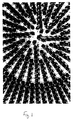
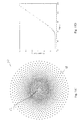
- Fig. 1 shows a diagram of the center of a conventional CMOS spatially variant imaging sensor.
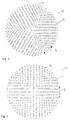
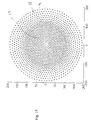
- Fig. 2 shows a substantially constant resolution sensor array in accordance with an embodiment of the present invention.
- Fig. 3 shows a substantially constant resolution sensor array in accordance with an embodiment of the present invention having an elliptical form.
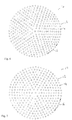
- Figs. 4 to 9 each show a substantially constant resolution sensor array in accordance with an embodiment of the present invention
- Fig. 10 is a graph showing the relationship between aspect ratio and symmetry m for substantially constant resolution sensor arrays in accordance with individual embodiments of the present invention
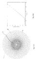
- Figs. 11A and B are, respectively, the representation of the sensor array and the variation of sensor spacing with radial distance in accordance with an embodiment of the present invention.
- Figs. 11C and 11D are, respectively, the representation of the sensor array and the variation of sensor spacing with radial distance in accordance with another embodiment of the present invention in which the sensor spacing merges gradually from the substantially constant resolution portion into the space variant portion.
- Figs. 12A and B are, respectively, the representation of the sensor array and the variation of sensor spacing with radial distance in accordance with another embodiment of the present invention in which the sensor spacing merges gradually from the substantially constant resolution portion into the space variant portion and back to a substantially constant resolution portion
- Figs. 13A and 13B show individual embodiments of sensor arrays including a substantially constant resolution portion and an outer space variant portion whereby in
- Fig. 13B the sensor location sites in each ring are displaced by one half of the site spacing compared to the previous ring.
- Figs. 14 and 15 show individual embodiments of sensor arrays including a substantially constant resolution portion and an outer space variant portion.
- Fig. 16 shows an embodiment of sensor location sites of a substantially constant resolution portion of a sensor array.
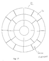
- Fig. 17 shows a further embodiment of sensor location sites of a substantially constant resolution portion of a sensor array.
- Aspect ratio the ratio between the radial and the angular distances dimension of each sensor element location site or of each sensor. Alternatively, the ratio between the mid-line to mid-line radial distance between neighboring rings and the angular distance between neighboring sensor element location sites or sensors.
- Sensor density number of sensor elements per unit area or the number of sensor element location sites per unit area. There can be a global and local density values.
- a global density is the density for the whole array or of a significant part of an array.
- Local density is the density of a small area of the array, e.g. defined by a sensor element location site or a sensor element and its neighbors. Sensor geometries with local discontinuities generally show local variations in local density.
- a log-polar array has a local resolution which varies linearly with radius.
- Resolution the inverse of the centre-centre distance between adjacent sensor element location sites or between sensor elements, for example it may be quoted as "dots per inch", "pixels per inch” or similar.
- a global resolution is the resolution typically possible for the whole array or for large part of an array.
- Local resolution is the centre-centre distance between sensor elements or sensor element location sites in a small area of the array, e.g. between one sensor element location site or sensor element and its neighbors. Sensor geometries with local discontinuities generally show local variations in local resolution.
- Closed smooth curve a closed figure which is non-polygonal. Examples are circle, ellipse, oval, egg-shape
- the present invention will be described with reference to certain embodiments and drawings but is not limited to these but only by the claims.
- the drawings are schematic.
- the present invention will mainly be described with reference to a radiation sensitive sensor array but the present invention is not limited thereto.
- the sensor element geometries of the present invention may be made with any suitable sensor elements, e.g. tactile sensor elements, proximity sensors.
- the present invention relates to the provision of a synthetic sensor array with a substantially constant resolution portion.
- synthetic is meant that natural sensor arrays such as the human eye are excluded.
- the substantially constant resolution portion may be used with a spatially variant portion which either surrounds the substantially constant resolution portion on the outside or is enclosed by the substantially constant resolution portion.
- CMOS or MOS semiconductor processing technology it is preferred in the present invention to use conventional CMOS or MOS semiconductor processing technology but the present invention is not limited thereto and includes other manufacturing technologies and devices made therefrom, such as CCD arrays.
- the present invention is not limited to visual light sensors but may be used with any radiation sensitive elements, e.g. those sensitive to X-rays or infra-red or ultraviolet radiation.
- sensor arrays in accordance with the present invention need not be radiation sensitive, they may be used, for instance, with tactile sensors, e.g. to model a synthetic finger tip.
- the sensors of the present invention may be conveniently manufactured in 0.35 micron CMOS technology but the present invention is not limited thereto.
- An individual sensor with such technology may have a diameter of about 7 micron.
- CMOS technology e.g. 0.35 micron
- An individual sensor with such technology may have a diameter of about 7 micron.
- electronic re-mapping e.g. log-polar mapping
- Such an array makes poor use of the large number of outer sensor elements as these are at the extremes of the field of view of a camera where high resolution is not so relevant.
- the number of these elements increases as the square of the radius so the total number of elements of such a uniform array compared to a space variant one is significantly larger. This increases processing time and therefore the cost of the sensor array.
- sensor element location sites 14 In the following reference will be made to sensor element location sites 14 and sensor elements. An example will be described for sensor element location sites with a symmetry of 6 (see below) but the skilled person will appreciate that the principles may be extended to a range of symmetries.
- Fig. 16 a series of concentric rings 16 of areas 14 is shown. These areas 14 are locations in which at least one sensor element is located hence they are sensor element location sites 14. More than one sensor element may be located in the each sensor element location site 14. Also a sensor element need not be located at the center of a sensor element location site 14. It is included within the present invention that a sensor element may be displaced from the center of a sensor element location, for example the displacements may be small, random in size and random in direction.
- Fig. 17 shows a further arrangement of sensor location sites 14.
- An embodiment of the present invention relates to a circular (polar) and regular arrangement of sensor element location sites 14 covering a bi-dimensional sensor array.
- Fig. 2 and following figures the center of each site 14 is marked with a dot.
- each site has an area determined by the bounds of the ring and its neighbors.
- sensor element location site 14 one or more sensor elements may be located.
- sensor elements are known, for example, from EP 739 039, EP 858 111, EP 773 669, for instance.
- This arrangement is intended primarily to implement at least one substantially constant resolution area 12 in a sensor 10 with a polar geometry (see Fig. 2).
- This constant resolution and polar arrangement is realized with sensor element location sites 14 arranged on concentric rings 16 which could be circles or any other closed curve, in particular closed, smooth curve, such as an ellipse as shown in Fig. 3 or an egg shape or an oval.
- “Substantially constant resolution” may be defined in accordance with the present invention as a polar array of sensor element locations 14 as described above wherein the radial displacement of any sensor element location site from a regular polar distribution is ⁇ 5% of the radius (defined by the distance from the center of the relevant ring) of the respective sensor element location site, more preferably ⁇ 3% of the radius and most preferably ⁇ 1% of the radius.
- the displacement of the sensor element location sites 14 from a regular polar distribution may be ⁇ 20% of the sensor element location site spacing in the angular direction (circumferential direction), more preferably ⁇ 10% and most preferably ⁇ 5% of the sensor element location site spacing in any ring.
- a substantially constant resolution portion 12 in accordance with an embodiment of the present invention may be characterized by a constant increase in the number of sensor element location sites per ring. For example if n (n ⁇ 1) is the number of sensor element location sites at the i th circle of an m- symmetric array, circle i+1 has n+m sensor element location sites.
- Various different symmetries are shown in Figs. 4 to 9.
- each ring 16 (other than the second ring) has m more sensor element location sites 14 than the ring inside it.
- the sensor element location sites 14 are distributed evenly along the ring.
- Figs. 4 to 9 show arrangements with m being 4, 5, 6, 7, 8, 9 respectively.
- each ring is calculated on the basis of equation 1.
- R n x 1/2 ⁇ + k
- R is the radius
- n is the number of sensor element location sites per ring
- 1 is the minimum center-centre distance between sensor element location sites around a ring
- k is a constant which is usually zero.
- the constant “k” effectively increases the dimension "1” by a fixed amount.
- the different symmetries shown are also characterized by the aspect ratio of each single sensory element locations.
- the aspect ratio of one sensor element location site may be defined as the ratio between the radial and the angular distances between the one sensor element location site and neighboring sensor element location sites or, alternatively, between the radial and the angular dimension of each single sensor element location sites.
- the spatial arrangement of constant resolution sensor element location sites 14 towards the outer diameter of the array is such that it may blend smoothly with a space-variant structure, such as an array of sensor element location sites with a log-polar density.
- a log polar mapping may be obtained by keeping the number of sensor element location sites per ring constant while the radius of each ring is defined in a log-polar manner, i.e. the ratio of the radii of adjacent ring is a constant. In such an arrangement the ratio of the diameters of adjacent rings is a constant.
- the outermost ring of the central constant resolution circular area 12 contains the same number of sensor element location sites as all the rings in the space-variant region 18.
- Figures 11 c and 11d show a further embodiment of the present invention in which an even smoother transition between the central constant resolution area 12 and the spatially variant peripheral part 18 of the array is obtained by sensor element location site spacing adjustments at the interface between region 12 and 18.
- the sensor element location site spacing may be gradually varied between the constant resolution portion and the spatially variant portion as shown in Fig.
- This gradual change may be defined by any suitable smoothing function. If the example of a log-polar mapping is taken for the spatially variant portion then the ratio of the outer diameters of adjacent rings is a constant in this portion. In the transition region between the constant resolution portion and the spatially variant portion this constant ratio of the radii of adjacent rings is changed smoothly from the value achieved at the outer ring of the constant resolution portion to the value in the body of the spatially variant portion.
- Constant resolution spatial arrangements in accordance with the present invention can be used not only for inner regions (as shown in Fig. 2) but also for annular regions 20 surrounding, for example, a space-variant circular region 18. This is shown in Figs. 12a and 12b in which there is a constant resolution portion 12 at the center and at the outer portion 20 of the sensor array with a log-polar arrangement in-between.
- the spatial arrangements for constant resolution areas of an image sensor have the following advantages:
- Sensor arrangements according to the present invention can be used as the basic sensor array of a color visual sensor.
- FIG. 13a An array with a quasi-square tessellation
- Fig. 13b An array with a quasi-hexagonal one
- each sensor element location site 14 includes one sensor element having a diameter of about 7 micron. This results in an diameter for the inner constant resolution portion of about 73 micron and about 100 micron for each design, respectively.
- the sensor arrays as described above in accordance with any of the embodiments of the present invention may find advantageous use in cameras, especially miniature cameras.
- Such cameras may be included in surveillance schemes such as for door or intruder surveillance, cameras for mounting in mobile telephones or lap-top or palm-top computers for capturing still and video images for transmission over telecommunications networks or similar, "eye-ball" cameras for mounting close to a Personal Computer for capturing still or video images and for transmission over telecommunications networks such as company Intranets, WAN's or the Internet or via telephone lines.
- the sensor arrays as described above may be associated with active or passive read-out electronics and digital signal processing circuitry to provide an electronic digital output of the image sensed by the array.
Landscapes
- Engineering & Computer Science (AREA)
- Multimedia (AREA)
- Signal Processing (AREA)
- Transforming Light Signals Into Electric Signals (AREA)
- Solid State Image Pick-Up Elements (AREA)
- Photometry And Measurement Of Optical Pulse Characteristics (AREA)
- Cameras In General (AREA)
Priority Applications (7)
| Application Number | Priority Date | Filing Date | Title |
|---|---|---|---|
| AT99203202T ATE450053T1 (de) | 1999-09-30 | 1999-09-30 | Sensormatrix mit einem bereich mit konstanter auflösung |
| DE69941698T DE69941698D1 (de) | 1999-09-30 | 1999-09-30 | Sensormatrix mit einem Bereich mit konstanter Auflösung |
| EP99203202A EP1089342B1 (de) | 1999-09-30 | 1999-09-30 | Sensormatrix mit einem Bereich mit konstanter Auflösung |
| US09/675,095 US7009645B1 (en) | 1999-09-30 | 2000-09-28 | Constant resolution and space variant sensor arrays |
| JP2000298896A JP2001160926A (ja) | 1999-09-30 | 2000-09-29 | センサアレイおよびカメラ |
| CA002321397A CA2321397A1 (en) | 1999-09-30 | 2000-09-29 | Constant resolution and space variant sensor arrays |
| US11/370,195 US20060215049A1 (en) | 1999-09-30 | 2006-03-07 | Constant resolution and space variant sensor arrays |
Applications Claiming Priority (1)
| Application Number | Priority Date | Filing Date | Title |
|---|---|---|---|
| EP99203202A EP1089342B1 (de) | 1999-09-30 | 1999-09-30 | Sensormatrix mit einem Bereich mit konstanter Auflösung |
Publications (2)
| Publication Number | Publication Date |
|---|---|
| EP1089342A1 true EP1089342A1 (de) | 2001-04-04 |
| EP1089342B1 EP1089342B1 (de) | 2009-11-25 |
Family
ID=8240697
Family Applications (1)
| Application Number | Title | Priority Date | Filing Date |
|---|---|---|---|
| EP99203202A Expired - Lifetime EP1089342B1 (de) | 1999-09-30 | 1999-09-30 | Sensormatrix mit einem Bereich mit konstanter Auflösung |
Country Status (5)
| Country | Link |
|---|---|
| EP (1) | EP1089342B1 (de) |
| JP (1) | JP2001160926A (de) |
| AT (1) | ATE450053T1 (de) |
| CA (1) | CA2321397A1 (de) |
| DE (1) | DE69941698D1 (de) |
Cited By (3)
| Publication number | Priority date | Publication date | Assignee | Title |
|---|---|---|---|---|
| FR2830128A1 (fr) * | 2001-09-26 | 2003-03-28 | Egg Solution Sa | Capteur photoelectrique avec des elements de capture de pixels disposes en cercles concentriques et dispositif d'acquisition d'images panoramiques comprenant ce capteur |
| WO2005057914A3 (en) * | 2003-12-05 | 2005-07-28 | Bae Systems Plc | Detection apparatus |
| US10580816B2 (en) | 2014-11-04 | 2020-03-03 | Sony Corporation | Solid-state imaging device, camera module, and electronic apparatus |
Families Citing this family (5)
| Publication number | Priority date | Publication date | Assignee | Title |
|---|---|---|---|---|
| JP4879513B2 (ja) * | 2005-05-17 | 2012-02-22 | 富士フイルム株式会社 | 撮像装置 |
| US8248499B2 (en) | 2009-02-23 | 2012-08-21 | Gary Edwin Sutton | Curvilinear sensor system |
| JP5270790B1 (ja) | 2012-05-30 | 2013-08-21 | 富士フイルム株式会社 | 放射線画像撮影装置、放射線画像撮影システム、放射線画像撮影装置の制御プログラム、及び放射線画像撮影装置の制御方法 |
| DE102016013510B4 (de) | 2016-04-18 | 2019-03-14 | Kastriot Merlaku | Scheinwerfer-System für Fahrzeuge aller Art, mit mindestens einem Leuchtmittel und eine Kamera für die Fahrbahn-Erfassung |
| CN115791917B (zh) * | 2022-11-10 | 2024-06-28 | 中国科学院长春应用化学研究所 | 圆形等面积单元划分方法及其在叉指电极分布中的应用 |
Citations (1)
| Publication number | Priority date | Publication date | Assignee | Title |
|---|---|---|---|---|
| US5587580A (en) * | 1994-10-25 | 1996-12-24 | Csem Centre Suisse D'electronique Et De Microtechnique Sa | Optoelectronic sensor for measuring the intensity and the direction of incidence of a light beam |
-
1999
- 1999-09-30 DE DE69941698T patent/DE69941698D1/de not_active Expired - Lifetime
- 1999-09-30 EP EP99203202A patent/EP1089342B1/de not_active Expired - Lifetime
- 1999-09-30 AT AT99203202T patent/ATE450053T1/de not_active IP Right Cessation
-
2000
- 2000-09-29 CA CA002321397A patent/CA2321397A1/en not_active Abandoned
- 2000-09-29 JP JP2000298896A patent/JP2001160926A/ja active Pending
Patent Citations (1)
| Publication number | Priority date | Publication date | Assignee | Title |
|---|---|---|---|---|
| US5587580A (en) * | 1994-10-25 | 1996-12-24 | Csem Centre Suisse D'electronique Et De Microtechnique Sa | Optoelectronic sensor for measuring the intensity and the direction of incidence of a light beam |
Non-Patent Citations (2)
| Title |
|---|
| PARDO F ET AL: "SPACE-VARIANT NONORTHOGONAL STRUCTURE CMOS IMAGE SENSOR DESIGN", IEEE JOURNAL OF SOLID-STATE CIRCUITS, vol. 33, no. 6, June 1998 (1998-06-01), IEEE, NEW YORK, US, pages 842 - 849, XP000833662, ISSN: 0018-9200 * |
| SCHEFFER D ET AL: "Log polar image sensor in CMOS technology", VISION SYSTEMS: SENSORS, SENSOR SYSTEMS, AND COMPONENTS, BESANCON, FRANCE, 10-12 JUNE 1996, vol. 2784, Proceedings of the SPIE - The International Society for Optical Engineering, 1996, SPIE-Int. Soc. Opt. Eng, USA, pages 2 - 11, XP002125828, ISSN: 0277-786X * |
Cited By (3)
| Publication number | Priority date | Publication date | Assignee | Title |
|---|---|---|---|---|
| FR2830128A1 (fr) * | 2001-09-26 | 2003-03-28 | Egg Solution Sa | Capteur photoelectrique avec des elements de capture de pixels disposes en cercles concentriques et dispositif d'acquisition d'images panoramiques comprenant ce capteur |
| WO2005057914A3 (en) * | 2003-12-05 | 2005-07-28 | Bae Systems Plc | Detection apparatus |
| US10580816B2 (en) | 2014-11-04 | 2020-03-03 | Sony Corporation | Solid-state imaging device, camera module, and electronic apparatus |
Also Published As
| Publication number | Publication date |
|---|---|
| CA2321397A1 (en) | 2001-03-30 |
| EP1089342B1 (de) | 2009-11-25 |
| JP2001160926A (ja) | 2001-06-12 |
| DE69941698D1 (de) | 2010-01-07 |
| ATE450053T1 (de) | 2009-12-15 |
Similar Documents
| Publication | Publication Date | Title |
|---|---|---|
| US7009645B1 (en) | Constant resolution and space variant sensor arrays | |
| US12087787B2 (en) | Solid-state image-capturing device and production method thereof, and electronic appliance | |
| US10666914B2 (en) | Solid state imaging device and electronic apparatus in which the area of the photodiode may be expanded | |
| JP5471117B2 (ja) | 固体撮像装置とその製造方法並びにカメラ | |
| US7538804B2 (en) | Solid state image pick-up device and image pick-up system | |
| US6665012B1 (en) | Process-scalable high spatial resolution and low bit resolution CMOS area image sensor | |
| TWI567955B (zh) | 用於次繞射極限感測器之色彩濾波器 | |
| US20190237496A1 (en) | Image sensor including a pixel block having 8-shared pixel structure | |
| US6838715B1 (en) | CMOS image sensor arrangement with reduced pixel light shadowing | |
| US10854649B2 (en) | Image sensor including unit pixel block having common selection transistor | |
| US20100320368A1 (en) | Color filters for sub-diffraction limit sensors | |
| JP3144537B2 (ja) | 固体撮像装置 | |
| EP1089342B1 (de) | Sensormatrix mit einem Bereich mit konstanter Auflösung | |
| KR102358317B1 (ko) | 이미지 센서 | |
| US12364035B2 (en) | Image sensor including a pixel array having pixel blocks arranged in a zigzag form | |
| US20220102401A1 (en) | Image sensing device | |
| US12035058B2 (en) | Electronic equipment | |
| US20240371903A1 (en) | Image sensor | |
| EP2304798B1 (de) | Bildsensorpixel mit grosser apertur | |
| EP0397272B1 (de) | Strahlungsempfindliche Vorrichtung in retinaähnlicher Konfiguration | |
| WO2022070815A1 (ja) | 撮像装置 | |
| JP5705462B2 (ja) | 固体撮像素子および電子情報機器 | |
| CN101278399B (zh) | 固态图像俘获装置及其制造方法和电子信息装置 | |
| US11483502B1 (en) | Bitline control supporting binning mode for pixel arrays with phase detection autofocus and image sensing photodiodes | |
| CN101512766B (zh) | 固态成像装置 |
Legal Events
| Date | Code | Title | Description |
|---|---|---|---|
| PUAI | Public reference made under article 153(3) epc to a published international application that has entered the european phase |
Free format text: ORIGINAL CODE: 0009012 |
|
| AK | Designated contracting states |
Kind code of ref document: A1 Designated state(s): AT BE CH CY DE DK ES FI FR GB GR IE IT LI LU MC NL PT SE |
|
| AX | Request for extension of the european patent |
Free format text: AL;LT;LV;MK;RO;SI |
|
| 17P | Request for examination filed |
Effective date: 20010914 |
|
| AKX | Designation fees paid |
Free format text: AT BE CH CY DE DK ES FI FR GB GR IE IT LI LU MC NL PT SE |
|
| AXX | Extension fees paid |
Free format text: AL PAYMENT 20010914;LT PAYMENT 20010914;LV PAYMENT 20010914;MK PAYMENT 20010914;RO PAYMENT 20010914;SI PAYMENT 20010914 |
|
| 17Q | First examination report despatched |
Effective date: 20070801 |
|
| GRAP | Despatch of communication of intention to grant a patent |
Free format text: ORIGINAL CODE: EPIDOSNIGR1 |
|
| RAP1 | Party data changed (applicant data changed or rights of an application transferred) |
Owner name: AITEK Owner name: IMEC |
|
| GRAS | Grant fee paid |
Free format text: ORIGINAL CODE: EPIDOSNIGR3 |
|
| GRAA | (expected) grant |
Free format text: ORIGINAL CODE: 0009210 |
|
| AK | Designated contracting states |
Kind code of ref document: B1 Designated state(s): AT BE CH CY DE DK ES FI FR GB GR IE IT LI LU MC NL PT SE |
|
| AX | Request for extension of the european patent |
Extension state: AL LT LV MK RO SI |
|
| REG | Reference to a national code |
Ref country code: GB Ref legal event code: FG4D |
|
| REG | Reference to a national code |
Ref country code: CH Ref legal event code: EP |
|
| REG | Reference to a national code |
Ref country code: IE Ref legal event code: FG4D |
|
| REF | Corresponds to: |
Ref document number: 69941698 Country of ref document: DE Date of ref document: 20100107 Kind code of ref document: P |
|
| REG | Reference to a national code |
Ref country code: NL Ref legal event code: VDEP Effective date: 20091125 |
|
| LTIE | Lt: invalidation of european patent or patent extension |
Effective date: 20091125 |
|
| PG25 | Lapsed in a contracting state [announced via postgrant information from national office to epo] |
Ref country code: SE Free format text: LAPSE BECAUSE OF FAILURE TO SUBMIT A TRANSLATION OF THE DESCRIPTION OR TO PAY THE FEE WITHIN THE PRESCRIBED TIME-LIMIT Effective date: 20091125 Ref country code: PT Free format text: LAPSE BECAUSE OF FAILURE TO SUBMIT A TRANSLATION OF THE DESCRIPTION OR TO PAY THE FEE WITHIN THE PRESCRIBED TIME-LIMIT Effective date: 20100325 Ref country code: FI Free format text: LAPSE BECAUSE OF FAILURE TO SUBMIT A TRANSLATION OF THE DESCRIPTION OR TO PAY THE FEE WITHIN THE PRESCRIBED TIME-LIMIT Effective date: 20091125 |
|
| PG25 | Lapsed in a contracting state [announced via postgrant information from national office to epo] |
Ref country code: CY Free format text: LAPSE BECAUSE OF FAILURE TO SUBMIT A TRANSLATION OF THE DESCRIPTION OR TO PAY THE FEE WITHIN THE PRESCRIBED TIME-LIMIT Effective date: 20091125 |
|
| PG25 | Lapsed in a contracting state [announced via postgrant information from national office to epo] |
Ref country code: BE Free format text: LAPSE BECAUSE OF FAILURE TO SUBMIT A TRANSLATION OF THE DESCRIPTION OR TO PAY THE FEE WITHIN THE PRESCRIBED TIME-LIMIT Effective date: 20091125 Ref country code: AT Free format text: LAPSE BECAUSE OF FAILURE TO SUBMIT A TRANSLATION OF THE DESCRIPTION OR TO PAY THE FEE WITHIN THE PRESCRIBED TIME-LIMIT Effective date: 20091125 |
|
| PG25 | Lapsed in a contracting state [announced via postgrant information from national office to epo] |
Ref country code: NL Free format text: LAPSE BECAUSE OF FAILURE TO SUBMIT A TRANSLATION OF THE DESCRIPTION OR TO PAY THE FEE WITHIN THE PRESCRIBED TIME-LIMIT Effective date: 20091125 Ref country code: ES Free format text: LAPSE BECAUSE OF FAILURE TO SUBMIT A TRANSLATION OF THE DESCRIPTION OR TO PAY THE FEE WITHIN THE PRESCRIBED TIME-LIMIT Effective date: 20100308 Ref country code: DK Free format text: LAPSE BECAUSE OF FAILURE TO SUBMIT A TRANSLATION OF THE DESCRIPTION OR TO PAY THE FEE WITHIN THE PRESCRIBED TIME-LIMIT Effective date: 20091125 |
|
| PLBE | No opposition filed within time limit |
Free format text: ORIGINAL CODE: 0009261 |
|
| STAA | Information on the status of an ep patent application or granted ep patent |
Free format text: STATUS: NO OPPOSITION FILED WITHIN TIME LIMIT |
|
| PG25 | Lapsed in a contracting state [announced via postgrant information from national office to epo] |
Ref country code: GR Free format text: LAPSE BECAUSE OF FAILURE TO SUBMIT A TRANSLATION OF THE DESCRIPTION OR TO PAY THE FEE WITHIN THE PRESCRIBED TIME-LIMIT Effective date: 20100226 |
|
| 26N | No opposition filed |
Effective date: 20100826 |
|
| PG25 | Lapsed in a contracting state [announced via postgrant information from national office to epo] |
Ref country code: IT Free format text: LAPSE BECAUSE OF FAILURE TO SUBMIT A TRANSLATION OF THE DESCRIPTION OR TO PAY THE FEE WITHIN THE PRESCRIBED TIME-LIMIT Effective date: 20091125 |
|
| PG25 | Lapsed in a contracting state [announced via postgrant information from national office to epo] |
Ref country code: MC Free format text: LAPSE BECAUSE OF NON-PAYMENT OF DUE FEES Effective date: 20100930 |
|
| REG | Reference to a national code |
Ref country code: CH Ref legal event code: PL |
|
| PG25 | Lapsed in a contracting state [announced via postgrant information from national office to epo] |
Ref country code: LI Free format text: LAPSE BECAUSE OF NON-PAYMENT OF DUE FEES Effective date: 20100930 Ref country code: IE Free format text: LAPSE BECAUSE OF NON-PAYMENT OF DUE FEES Effective date: 20100930 Ref country code: CH Free format text: LAPSE BECAUSE OF NON-PAYMENT OF DUE FEES Effective date: 20100930 |
|
| PG25 | Lapsed in a contracting state [announced via postgrant information from national office to epo] |
Ref country code: LU Free format text: LAPSE BECAUSE OF NON-PAYMENT OF DUE FEES Effective date: 20100930 |
|
| REG | Reference to a national code |
Ref country code: FR Ref legal event code: PLFP Year of fee payment: 18 |
|
| REG | Reference to a national code |
Ref country code: FR Ref legal event code: PLFP Year of fee payment: 19 |
|
| REG | Reference to a national code |
Ref country code: FR Ref legal event code: PLFP Year of fee payment: 20 |
|
| PGFP | Annual fee paid to national office [announced via postgrant information from national office to epo] |
Ref country code: FR Payment date: 20180822 Year of fee payment: 20 Ref country code: DE Payment date: 20180821 Year of fee payment: 20 |
|
| PGFP | Annual fee paid to national office [announced via postgrant information from national office to epo] |
Ref country code: GB Payment date: 20180823 Year of fee payment: 20 |
|
| REG | Reference to a national code |
Ref country code: DE Ref legal event code: R071 Ref document number: 69941698 Country of ref document: DE |
|
| REG | Reference to a national code |
Ref country code: GB Ref legal event code: PE20 Expiry date: 20190929 |
|
| PG25 | Lapsed in a contracting state [announced via postgrant information from national office to epo] |
Ref country code: GB Free format text: LAPSE BECAUSE OF EXPIRATION OF PROTECTION Effective date: 20190929 |