EP1089375A2 - Module de circuit à haute fréquence et dispositif de communication - Google Patents
Module de circuit à haute fréquence et dispositif de communication Download PDFInfo
- Publication number
- EP1089375A2 EP1089375A2 EP00117292A EP00117292A EP1089375A2 EP 1089375 A2 EP1089375 A2 EP 1089375A2 EP 00117292 A EP00117292 A EP 00117292A EP 00117292 A EP00117292 A EP 00117292A EP 1089375 A2 EP1089375 A2 EP 1089375A2
- Authority
- EP
- European Patent Office
- Prior art keywords
- dielectric substrate
- ground metal
- layer dielectric
- high frequency
- conductor
- Prior art date
- Legal status (The legal status is an assumption and is not a legal conclusion. Google has not performed a legal analysis and makes no representation as to the accuracy of the status listed.)
- Granted
Links
Images





Classifications
-
- H—ELECTRICITY
- H05—ELECTRIC TECHNIQUES NOT OTHERWISE PROVIDED FOR
- H05K—PRINTED CIRCUITS; CASINGS OR CONSTRUCTIONAL DETAILS OF ELECTRIC APPARATUS; MANUFACTURE OF ASSEMBLAGES OF ELECTRICAL COMPONENTS
- H05K1/00—Printed circuits
- H05K1/18—Printed circuits structurally associated with non-printed electric components
-
- H—ELECTRICITY
- H01—ELECTRIC ELEMENTS
- H01P—WAVEGUIDES; RESONATORS, LINES, OR OTHER DEVICES OF THE WAVEGUIDE TYPE
- H01P3/00—Waveguides; Transmission lines of the waveguide type
- H01P3/02—Waveguides; Transmission lines of the waveguide type with two longitudinal conductors
- H01P3/08—Microstrips; Strip lines
- H01P3/088—Stacked transmission lines
-
- H—ELECTRICITY
- H10—SEMICONDUCTOR DEVICES; ELECTRIC SOLID-STATE DEVICES NOT OTHERWISE PROVIDED FOR
- H10W—GENERIC PACKAGES, INTERCONNECTIONS, CONNECTORS OR OTHER CONSTRUCTIONAL DETAILS OF DEVICES COVERED BY CLASS H10
- H10W44/00—Electrical arrangements for controlling or matching impedance
- H10W44/20—Electrical arrangements for controlling or matching impedance at high-frequency [HF] or radio frequency [RF]
- H10W44/241—Electrical arrangements for controlling or matching impedance at high-frequency [HF] or radio frequency [RF] for passive devices or passive elements
- H10W44/248—Electrical arrangements for controlling or matching impedance at high-frequency [HF] or radio frequency [RF] for passive devices or passive elements for antennas
-
- H—ELECTRICITY
- H10—SEMICONDUCTOR DEVICES; ELECTRIC SOLID-STATE DEVICES NOT OTHERWISE PROVIDED FOR
- H10W—GENERIC PACKAGES, INTERCONNECTIONS, CONNECTORS OR OTHER CONSTRUCTIONAL DETAILS OF DEVICES COVERED BY CLASS H10
- H10W72/00—Interconnections or connectors in packages
- H10W72/851—Dispositions of multiple connectors or interconnections
- H10W72/874—On different surfaces
- H10W72/884—Die-attach connectors and bond wires
-
- H—ELECTRICITY
- H10—SEMICONDUCTOR DEVICES; ELECTRIC SOLID-STATE DEVICES NOT OTHERWISE PROVIDED FOR
- H10W—GENERIC PACKAGES, INTERCONNECTIONS, CONNECTORS OR OTHER CONSTRUCTIONAL DETAILS OF DEVICES COVERED BY CLASS H10
- H10W90/00—Package configurations
- H10W90/701—Package configurations characterised by the relative positions of pads or connectors relative to package parts
- H10W90/731—Package configurations characterised by the relative positions of pads or connectors relative to package parts of die-attach connectors
- H10W90/734—Package configurations characterised by the relative positions of pads or connectors relative to package parts of die-attach connectors between a chip and a stacked insulating package substrate, interposer or RDL
-
- H—ELECTRICITY
- H10—SEMICONDUCTOR DEVICES; ELECTRIC SOLID-STATE DEVICES NOT OTHERWISE PROVIDED FOR
- H10W—GENERIC PACKAGES, INTERCONNECTIONS, CONNECTORS OR OTHER CONSTRUCTIONAL DETAILS OF DEVICES COVERED BY CLASS H10
- H10W90/00—Package configurations
- H10W90/701—Package configurations characterised by the relative positions of pads or connectors relative to package parts
- H10W90/751—Package configurations characterised by the relative positions of pads or connectors relative to package parts of bond wires
- H10W90/754—Package configurations characterised by the relative positions of pads or connectors relative to package parts of bond wires between a chip and a stacked insulating package substrate, interposer or RDL
Definitions
- the present invention relates to a high frequency circuit module and a communication device such as a mobile wireless terminal and a pocket telephone using it.
- a high frequency circuit module used for a communication device such as conventional type mobile wireless terminal and pocket telephone
- the one using a single layer or multi-layer dielectric substrate is known.
- first conventional technique An example of a high frequency circuit module using a single layer dielectric substrate is shown in the proceeding of the 1996 Institute IEIC Spring Conference C-86, "A Power Amplifier Using Single Layer Alumina Substrate with Thin-Film Resistors and Capacitors for North American Digital Phone System" (hereinafter called first conventional technique).
- a transmission line which is a distributed element, a lumped constant element such as a resistor, a capacitor and an inductor and a semiconductor element are formed on the same surface of a dielectric substrate to compose an input-output matching circuit and a power amplifier.
- a high frequency signal is transmitted to an external device by a high frequency signal electrode provided to the surface of the dielectric substrate.
- the earth electrode of the semiconductor element provided to the surface of the dielectric substrate and an earth electrode on the reverse side are connected via a through-hole.
- a transmission line which is a distributed constant element, an input-output matching circuit composed of a lumped constant element such as a resistor, a capacitor and an inductor and a semiconductor element are formed on the same surface of a dielectric substrate to compose a high frequency circuit module.
- a high frequency signal electrode provided to the surface of a first layer of the dielectric substrate and a high frequency signal electrode on the reverse side of a second layer are connected via wiring provided to the surface of the second layer through a through-hole.
- the earth electrode of the semiconductor element provided to the surface of the first layer of the dielectric substrate and an earth electrode on the reverse side are connected via a through-hole.
- the order of the layers of the dielectric substrate are counted as a first layer, a second layer, a third layer, --- from the surface to the reverse side.
- Fig. 9 is a general schematic sectional view showing a transmission line formed on a single layer dielectric substrate.
- a conductor 43 on the surface, a dielectric substrate 44 and ground metal on the reverse side 45 forms a transmission line.
- Fig. 10 shows calculated values of transmission loss at the frequency of 1.9 GHz when the relative dielectric constant of the dielectric substrate 44 is 8.1 and the thickness of the dielectric substrate 44 is varied from 0.1 mm to 3.0 mm.
- Curves 1 to 3 show cases in which the width of the conductor 43 forming a transmission line is respectively 0.1 mm, 0.2 mm and 0.5 mm.
- the transmission loss has a tendency to become small.
- Fig. 11 shows calculated values of transmission loss at the frequency of 1.9 GHz when the relative inductivity of the dielectric substrate 44 is 8.1 and the width of the conductor 43 forming a transmission line is varied from 0.02 mm to 3.0 mm.
- Curves 1 to 3 show cases in which the thickness of the dielectric substrate 44 is respectively 0.15 mm, 0.3 mm and 0.6 mm.
- the transmission loss decreases as the conductor 43 forming a transmission line becomes wide, becomes minimum in a range in which the width of the conductor 43 is 0.3 to 0.7 mm and increases when the conductor 43 becomes wider.
- Fig. 12 is a general schematic sectional view showing a transmission line formed on a two-layer dielectric substrate.
- a conductor 46, a dielectric substrate 47, ground metal 48 on the reverse side and ground metal 49 on the surface forms a transmission line.
- Fig. 13 shows calculated values of transmission loss at the frequency of 1.9 GHz when the relative dielectric constant of the dielectric substrate 47 is 8.1 and the thickness of the dielectric substrate 47 is varied from 0.1 mm to 3.0 mm.
- Curves 1 to 3 show cases in which the width of the conductor 46 forming a transmission line is respectively 0.1 mm, 0.2 mm and 0.5 mm. As clear from Fig. 13, in the cases of any width of the conductor 46, as the dielectric substrate 47 becomes thick, the transmission loss becomes small.
- Fig. 14 shows calculated values of transmission loss at the frequency of 1.9 GHz when the relative inductivity of the dielectric substrate 47 is 8.1 and the width of the conductor 46 forming a transmission line is varied from 0.02 mm to 3.0 mm.
- Curves 1 to 3 show cases in which the thickness of the dielectric substrate 47 is respectively 0.15 mm, 0.3 mm and 0.6 mm.
- the transmission loss has a tendency to become small.
- the object of this invention is to provide a high frequency circuit module which can be more miniaturized and a communication device using it.
- a high frequency circuit module uses a two or more-layer dielectric substrate and the thickness of the dielectric substrate between a conductor forming the transmission line of a matching circuit on the side of input or output and ground metal is composed of two or more layers.
- the ground metal provided to the dielectric substrate between them is formed in the shape in which a part is hollowed out so that a part opposite to the conductor is included.
- the transmission loss can be reduced, and a high frequency circuit module and a communication device using it can be miniaturized.
- Fig. 1 is an exploded view showing a high frequency circuit module equivalent to a first embodiment.
- a matching circuit on the input side composed of conductor line 2 and chip capacitors 3, 4 and 5 and a matching circuit on the output side composed of conductor line 9 and chip capacitors 10, 11 and 12 are formed on the surface of a first-layer dielectric substrate 1, a matching circuit on the input side composed of conductor line 2 and chip capacitors 3, 4 and 5 and a matching circuit on the output side composed of conductor line 9 and chip capacitors 10, 11 and 12 are formed.
- the chip capacitor 3 is connected to an input terminal 8
- the chip capacitor 4 is connected to an earth terminal 6
- the chip capacitor 5 is connected to an earth terminal 7
- the chip capacitor 10 is connected to an output terminal 15
- the chip capacitor 11 is connected to an earth terminal 13 and the chip capacitor 12 is connected to an earth terminal 14.
- a through-hole 17 piercing the first-layer dielectric substrate 1 is provided to the dielectric substrate.
- a semiconductor chip 16 is bonded to ground metal 19 provided on
- the conductor line 2 on the surface of the first-layer dielectric substrate 1 is connected to one end of conductor line 25 provided on the surface of a third-layer dielectric substrate 24 via a through-hole 120 provided to the first-layer dielectric substrate 1 and a through-hole 20 provided to the second-layer dielectric substrate 18.
- the other end of the line 25 is connected to a terminal 26 provided on the surface of the first-layer dielectric substrate 1 via a through-hole 21 provided to the second-layer dielectric substrate 18 and a through-hole 121 provided to the first-layer dielectric substrate 1.
- the conductor line 9 on the surface of the first-layer dielectric substrate 1 is connected to one end of a conductor line 31 provided on the surface of a fourth-layer dielectric substrate 30 via a through-hole 122 provided to the first-layer dielectric substrate 1, a through-hole 22 provided to the second-layer dielectric substrate 18 and a through-hole 27 provided to the third-layer dielectric substrate 24.
- the other end of the conductor line 31 is connected to a terminal 32 provided on the surface of the first-layer dielectric substrate 1 via a through-hole 28 provided to the third-layer dielectric substrate 24, a through-hole 23 provided to the second-layer dielectric substrate 18 and a through-hole 123 provided to the first-layer dielectric substrate 1.
- the semiconductor chip 16 is bonded to the conductor lines 2 and 9 on the surface of the first-layer dielectric substrate 1.
- the ground metal 19 on the surface of the second-layer dielectric substrate 18 to which the semiconductor chip 16 is bonded is connected to ground metal 29 provided on the surface of the third-layer dielectric substrate 24, ground metal 33 provided on the surface of the fourth-layer dielectric substrate 30 and ground metal 34 provided on the reverse side of the fourth-layer dielectric substrate 30 via a through-hole 151 provided to the second-layer dielectric substrate 18, a through-hole 152 provided to the third-layer dielectric substrate 24, a through-hole 153 provided to the fourth-layer dielectric substrate 30 and a through-hole 154 provided to the ground metal 34 on the reverse side of the fourth-layer dielectric substrate 30.
- Each rectangular frame respectively surrounding the through-holes 151, 152, 153 and 154 shows an area where the semiconductor chip 16 is to be installed.
- a part 35 of the ground metal 19 on the surface of the second-layer dielectric substrate 18 is removed so that a part opposite to the conductor line 9 of the matching circuit on the output side on the surface of the first-layer dielectric substrate 1 is included.
- the ground metal 19 is connected to the ground metal 29, 36 and 37 provided on the surface of the third-layer dielectric substrate 24, the ground metal 33, 38 and 39 provided on the surface of the fourth-layer dielectric substrate 30 and the ground metal 34 provided on the reverse side of the fourth-layer dielectric substrate 30 via through-holes (no reference number) provided in the periphery of the second-, third- and fourth-layer dielectric substrates 18, 24 and 30 and through-holes (no reference number) provided in the periphery of the ground metal 34 provided on the reverse side of the fourth-layer dielectric substrate 30.
- each ground metal and each through-hole are connected by forming each ground metal by copper and embodying copper in each through-hole.
- the first-layer dielectric substrate 1 and the second-layer dielectric substrate 18 continue between the conductor line 9 and the ground metal 29, and for the thickness between both, the thickness of the second-layer dielectric substrate 18 is added to that of the first-layer dielectric substrate 1. Therefore, the thickness between the conductor line 9 and the ground metal 29 can be thicker than the thickness of only the first-layer dielectric substrate 1 or the second-layer dielectric substrate 18 and the transmission loss can be reduced.
- the terminals 8 and 15 via which a high frequency signal is input/output and the terminals 26 and 32 via which voltage is applied to the semiconductor chip 16 are provided on the surface of the first-layer dielectric substrate 1, however, for example, a terminal via which a high frequency signal is input/output may be also provided on the surface of the first-layer dielectric substrate 1 and a terminal via which voltage is applied to the semiconductor chip 16 may be also provided on the reverse side of the fourth-layer dielectric substrate 30. Also, a terminal via which a high frequency signal is input/output and a terminal via which voltage is applied to the semiconductor chip 16 may be also provided on the reverse side of the fourth-layer dielectric substrate 30. And the number of terminals is also not particularly limited.
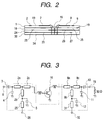
- Fig. 2 is a sectional view viewed along a line II-II in case the dielectric substrates shown in Fig. 1 are assembled.
- the dielectric substrate in the part 35 can be thicker than the first-layer dielectric substrate 1, the second-layer dielectric substrate 18, the third-layer dielectric substrate 24 and the fourth-layer dielectric substrate 30 by providing the part 35 formed by removing a part of the ground metal 19 on the surface of the second-layer dielectric substrate 18.
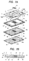
- Fig. 3 shows an equivalent circuit of a single-stage amplifier of the high frequency circuit module shown in Fig. 1. It includes a matching circuit on the input side composed of the conductor line 2, chip capacitors 3, 4 and 5, a line 25 that applies power supply voltage to the semiconductor chip 16 including bonding wire, a power supply voltage terminal 26 and an input terminal 8 and a matching circuit on the output side composed of a conductor line 9, chip capacitors 10, 11 and 12, a line 31 that applies power supply voltage to the semiconductor chip 16 including bonding wire, a power supply voltage terminal 32 and an output terminal 15.
- the conductor line 2 is composed of a conductor lines 2a, 2b and 2c and the conductor line 9 is composed of conductor lines 9a, 9b and 9c.
- Fig. 4 shows the loss of the matching circuit in case the equivalent circuit of the matching circuit on the output side shown in Fig. 3 is composed of a single layer dielectric substrate 44 as shown in Fig. 9, the output impedance of the semiconductor chip 16 including bonding wire is 1 to 100 ⁇ , load impedance is 50 ⁇ , the relative inductivity of the dielectric substrate 44 is 8.1, the width of the conductor line 9 formed on the dielectric substrate 44 is 0.3 mm, the dielectric loss tangent tan ⁇ of the dielectric substrate 44 is 0.017, the length of the conductor lines 9a, 9b and 9c and the values of the chip capacitors 10, 11 and 12 are optimized so that they are matched at the frequency of 1.9 GHz. As shown in Fig.
- curves 1, 2 and 3 show calculated values in case the thickness of the dielectric substrate 44 is respectively 0.15 mm, 0.3 mm and 0.6 mm.
- the loss of the matching circuit has a tendency to become small.
- the loss of the matching circuit is 0.16 dB in case the thickness of the dielectric substrate 44 is 0.15 mm, however, when the thickness of the dielectric substrate 44 is 0.3 mm, the loss of the matching circuit is 0.13 dB and when the thickness of the dielectric substrate 44 is 0.6 mm, the loss of the matching circuit is reduced up to 0.1 dB.
- Fig. 5A is an exploded view showing a high frequency circuit module equivalent to a second embodiment and Fig. 5B is a sectional view viewed along a line VB-VB in case the high frequency circuit module shown in Fig. 5A is assembled.
- a matching circuit on the input side composed of a conductor line 2 and chip capacitors 3, 4 and 5 is formed on a first-layer dielectric substrate 1, the chip capacitor 3 is connected to an input terminal 8, the chip capacitor 4 is connected to an earth terminal 6 and the chip capacitor 5 is connected to an earth terminal 7.
- the input terminal 8 is connected to a terminal 8c provided by removing ground metal formed on the reverse side of a third-layer dielectric substrate 24 via a through-hole 8a provided to a second-layer dielectric substrate 18 and a through-hole 8b provided to the third-layer dielectric substrate 24. Further, a matching circuit on the output side composed of a conductor line 9 and chip capacitors 10, 11 and 12 is formed, the chip capacitor 10 is connected to an output terminal 15, the chip capacitor 11 is connected to an earth terminal 13 and the chip capacitor 12 is connected to an earth terminal 14.
- the output terminal 15 is connected to a terminal 15c provided by removing ground metal formed on the reverse side of the third-layer dielectric substrate 24 via a through-hole 15a provided to the second-layer dielectric substrate 18 and a through-hole 15b provided to the third-layer dielectric substrate 24.
- a dielectric substance is removed and a hole 17 that pierces the dielectric substrate is provided to the first-layer dielectric substrate 1.
- the conductor line 2 provided on the surface of the first-layer dielectric substrate 1 is connected to a terminal 26.
- the conductor line 9 provided on the surface of the first-layer dielectric substrate 1 is connected to a terminal 32.
- the semiconductor chip 16 is bonded to the conductor lines 2 and 9 provided on the surface of the first-layer dielectric substrate 1.
- the ground metal 19 formed on the surface of the second-layer dielectric substrate 18 to which the semiconductor chip 16 is bonded is connected to ground metal 29 provided on the surface of the third-layer dielectric substrate 24 and ground metal 34 formed on the reverse side of the third-layer dielectric substrate 24 via through-holes in a part where the semiconductor chip 16 is bonded.
- a part 35 of the ground metal 19 formed on the surface of the second-layer dielectric substrate 18 is removed so that a part opposite to the conductor line 9 of the matching circuit on the output side formed on the surface of the first-layer dielectric substrate 1 is included.
- the ground metal 19 is connected to the ground metal 29 and 34 respectively formed on the surface and on the reverse side of the third-layer dielectric substrate 24 via through-holes in the periphery of the dielectric substrate.
- Fig. 6A is an exploded view showing a high frequency circuit module equivalent to a third embodiment and Fig. 6B is a sectional view viewed along a line VIB-VIB in case the high frequency circuit module shown in Fig. 6A is assembled.
- a matching circuit on the input side composed of a conductor line 2 and chip capacitors 3, 4 and 5 is formed on the surface of a first-layer dielectric substrate 1, the chip capacitor 3 is connected to an input terminal 8, the chip capacitor 4 is connected to an earth terminal 6 and the chip capacitor 5 is connected to an earth terminal 7.
- the input terminal 8 is connected to a terminal 8c provided by removing ground metal formed on the reverse side of a third-layer dielectric substrate 24 via a through-hole 8a provided to a second-layer dielectric substrate 18 and a through-hole 8b provided to the third-layer dielectric substrate 24. Further, a matching circuit on the output side composed of a conductor line 9 and chip capacitors 10, 11 and 12 is formed, the chip capacitor 10 is connected to an output terminal 15, the chip capacitor 11 is connected to an earth terminal 13 and the chip capacitor 12 is connected to an earth terminal 14.
- the output terminal 15 is connected to a terminal 15c provided by removing ground metal 34 formed on the reverse side of the third-layer dielectric substrate 24 via a through-hole 15a provided to the second-layer dielectric substrate 18 and a through-hole 15b provided to the third-layer dielectric substrate 24.
- a dielectric substance is removed and a hole 17 that pierces the dielectric substrate is provided to the first-layer dielectric substrate 1.
- the conductor line 2 provided on the first-layer dielectric substrate 1 is connected to a terminal 26.
- the conductor line 9 provided on the surface of the first-layer dielectric substrate 1 is connected to a terminal 32.
- the semiconductor chip 16 is bonded to the conductor lines 2 and 9 provided on the surface of the first-layer dielectric substrate 1.
- the ground metal 19 formed on the surface of the second-layer dielectric substrate 18 to which the semiconductor chip 16 is bonded is connected to ground metal 29 and 34 provided on the surface and on the reverse side of the third-layer dielectric substrate 24 via through-holes in a part where the semiconductor chip 16 is bonded.
- a part 35 of the ground metal 19 formed on the surface of the second-layer dielectric substrate 18 is removed so that a part opposite to the conductor line 9 of the matching circuit on the output side formed on the surface of the first-layer dielectric substrate 1 is included. Further, a part 40 of the ground metal 29 on the surface of the third-layer dielectric substrate 24 is removed so that a part opposite to the conductor line 9 is included.
- the ground metal 19 and 29 are connected to each other via through-holes in the periphery of the dielectric substrate and is also connected to the ground metal 34 formed on the reverse side of the third-layer dielectric substrate 24.
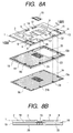
- Fig. 7A is an exploded view showing a high frequency circuit module equivalent to a fourth embodiment and Fig. 7B is a sectional view viewed along a line VIIB-VIIB in case the high frequency circuit module shown in Fig. 7A is assembled.
- a matching circuit on the input side composed of a conductor line 2 and chip capacitors 3, 4 and 5 is formed on the surface of a first-layer dielectric substrate 1, the chip capacitor 3 is connected to an input terminal 8, the chip capacitor 4 is connected to an earth terminal 6 and the chip capacitor 5 is connected to an earth terminal 7.
- the input terminal 8 is connected to a terminal 8c provided by removing ground metal formed on the reverse side of a third-layer dielectric substrate 24 via a through-hole 8a provided to a second-layer dielectric substrate 18 and a through-hole 8b provided to the third-layer dielectric substrate 24. Further, a matching circuit on the output side composed of a conductor line 9 and chip capacitors 10, 11 and 12 is formed, the chip capacitor 10 is connected to an output terminal 15, the chip capacitor 11 is connected to an earth terminal 13 and the chip capacitor 12 is connected to an earth terminal 14.
- the output terminal 15 is connected to a terminal 15c provided by removing ground metal formed on the reverse side of the third-layer dielectric substrate 24 via a through-hole 15a provided to the second-layer dielectric substrate 18 and a through-hole 15b provided to the third-layer dielectric substrate 24.
- a dielectric substance is removed and a hole 17 that pierces the dielectric substrate is provided to the first-layer dielectric substrate 1.
- the conductor line 2 provided on the first-layer dielectric substrate 1 is connected to a terminal 26.
- the conductor line 9 provided on the surface of the first-layer dielectric substrate 1 is connected to a terminal 32.
- the semiconductor chip 16 is bonded to the conductor lines 2 and 9 provided on the surface of the first-layer dielectric substrate 1.
- the ground metal 19 formed on the surface of the second-layer dielectric substrate 18 to which the semiconductor chip 16 is bonded is connected to ground metal 29 and 34 provided on the surface and on the reverse side of the third-layer dielectric substrate 24 via through-holes in a part where the semiconductor chip 16 is bonded.
- a part 41 of the ground metal 19 on the surface of the second-layer dielectric substrate 18 is removed so that a part opposite to the conductor line 2 of the matching circuit on the input side on the surface of the first-layer dielectric substrate 1 is included. Further, a part 35 of the ground metal 19 on the surface of the second-layer dielectric substrate 18 is removed so that a part opposite to the conductor line 9 of the matching circuit on the output side is included.
- the dielectric substrate in the removed part can be thicker than the first-layer dielectric substrate 1, the second-layer dielectric substrate 18 or the third-layer dielectric substrate 24.
- the ground metal 19 is connected to the ground metal 29 and 34 formed on the surface and on the reverse side of the third-layer dielectric substrate 24 via through-holes in the periphery of the dielectric substrate.
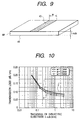
- Fig. 8A is an exploded view showing a high frequency circuit module equivalent to a fifth embodiment and Fig. 8B is a sectional view viewed along a line VIIIB-VIIIB in case the high frequency circuit module shown in Fig. 8A is assembled.
- a matching circuit on the input side composed of a conductor line 2 and chip capacitors 3, 4 and 5 is formed on the surface of a first-layer dielectric substrate 1, the chip capacitor 3 is connected to an input terminal 8, the chip capacitor 4 is connected to an earth terminal 6 and the chip capacitor 5 is connected to an earth terminal 7.
- the input terminal 8 is connected to a terminal 8c provided by removing ground metal formed on the reverse side of a second-layer dielectric substrate 18 via a through-hole 8a provided to the second-layer dielectric substrate 18.
- a matching circuit on the output side composed of a conductor line 9 and chip capacitors 10, 11 and 12 is formed, the chip capacitor 10 is connected to an output terminal 15, the chip capacitor 11 is connected to an earth terminal 13 and the chip capacitor 12 is connected to an earth terminal 14.
- the output terminal 15 is connected to a terminal 15c provided by removing ground metal formed on the reverse side of the second-layer dielectric substrate 18 via a through-hole 15b provided to the second-layer dielectric substrate 18.
- a dielectric substance is removed and a hole 17 that pierces the dielectric substrate is provided to the first-layer dielectric substrate 1.
- the conductor line 2 provided on the surface of the first-layer dielectric substrate 1 is connected to a terminal 26.
- the conductor line 9 provided on the surface of the first-layer dielectric substrate 1 is connected to a terminal 32.
- the semiconductor chip 16 is bonded to the conductor lines 2 and 9 provided on the surface of the first-layer dielectric substrate 1.
- the ground metal 19 formed on the surface of the second-layer dielectric substrate 18 to which the semiconductor chip 16 is bonded is connected to ground metal 29 provided on the reverse side of the second-layer dielectric substrate 18 via through-holes in a part where the semiconductor chip 16 is bonded.
- a part 35 of the ground metal 19 on the surface of the second-layer dielectric substrate 18 is removed so that a part opposite to the conductor line 9 of the matching circuit on the output side on the surface of the first-layer dielectric substrate 1 is included.
- the dielectric substrate in the removed part can be thicker than the first-layer dielectric substrate 1 or the second-layer dielectric substrate 18.
- the ground metal 19 is connected to the ground metal 29 formed on the reverse side of the second-layer dielectric substrate 18 via through-holes in the periphery of the dielectric substrate.
- Fig. 15 is a block diagram showing a mobile wireless terminal equivalent to one embodiment of a communication device according to the invention.
- Fig. 16 is a part layout drawing showing a high frequency unit of the mobile wireless terminal shown in Fig. 15.
- a signal at the transmitting end is output from an antenna-2 102 via a modulator 108, a burst switch 107, a driving amplifier 106, a filter 105, a power amplifier 104 and a duplexer 103.
- a diversity system in which a case that a signal is received from an antenna-1 101 and is transmitted via a low noise amplifier 109, a filter 105, a frequency converter 110 and an IF amplifier 111 and a case that a signal is received from the antenna-2 102 and is transmitted via a low noise amplifier 109, a filter 105, a frequency converter 110 and an IF amplifier 111 are compared, a received signal is processed in a demodulation unit 113 and reaches a base band unit 114 is adopted.
- a reference number 112 denotes a frequency synthesizer.
- the high frequency circuit module described in any of the first to fifth embodiments is used for the power amplifier 104 and a low noise amplifier 109.
- the high frequency circuit module that the dielectric substrate between the conductor line of the matching circuit on the input side and the ground metal is also composed of two or more layers is used in addition to the high frequency circuit module that the dielectric substrate between the conductor line of the matching circuit on the output side and the ground metal is composed of two or more layers.
- the high frequency circuit module that the dielectric substrate between the conductor line of the matching circuit on the output side and the ground metal is also composed of two or more layers is used in addition to the high frequency circuit module that the dielectric substrate between the conductor line of the matching circuit on the input side and the ground metal is composed of two or more layers.
- the mobile wireless terminal can be miniaturized by using these high frequency circuit modules.
Landscapes
- Engineering & Computer Science (AREA)
- Microelectronics & Electronic Packaging (AREA)
- Microwave Amplifiers (AREA)
- Transceivers (AREA)
Applications Claiming Priority (2)
| Application Number | Priority Date | Filing Date | Title |
|---|---|---|---|
| JP27573099 | 1999-09-29 | ||
| JP27573099A JP3976297B2 (ja) | 1999-09-29 | 1999-09-29 | 高周波回路モジュールおよび通信装置 |
Publications (3)
| Publication Number | Publication Date |
|---|---|
| EP1089375A2 true EP1089375A2 (fr) | 2001-04-04 |
| EP1089375A3 EP1089375A3 (fr) | 2002-12-11 |
| EP1089375B1 EP1089375B1 (fr) | 2008-05-14 |
Family
ID=17559596
Family Applications (1)
| Application Number | Title | Priority Date | Filing Date |
|---|---|---|---|
| EP00117292A Expired - Lifetime EP1089375B1 (fr) | 1999-09-29 | 2000-08-17 | Module de circuit à haute fréquence et dispositif de communication |
Country Status (5)
| Country | Link |
|---|---|
| US (1) | US6753604B1 (fr) |
| EP (1) | EP1089375B1 (fr) |
| JP (1) | JP3976297B2 (fr) |
| KR (1) | KR100711175B1 (fr) |
| DE (1) | DE60038854D1 (fr) |
Cited By (3)
| Publication number | Priority date | Publication date | Assignee | Title |
|---|---|---|---|---|
| EP1414279A3 (fr) * | 2002-10-23 | 2006-10-25 | Murata Manufacturing Co., Ltd. | Module à haute fréquence et appareil de communication |
| EP3109898A1 (fr) * | 2015-06-22 | 2016-12-28 | NXP USA, Inc. | Circuit radiofrequence avec un substrat radiofrequence multicouche qui contient un plan de masse électriquement conducteur avec un espace vide en dessous d'une piste de polarisation |
| CN114725642A (zh) * | 2022-03-16 | 2022-07-08 | 天津大学 | 针对介质集成悬置线和金属-介质集成悬置线有源器件的封装结构 |
Families Citing this family (12)
| Publication number | Priority date | Publication date | Assignee | Title |
|---|---|---|---|---|
| JP3941416B2 (ja) | 2001-04-26 | 2007-07-04 | ソニー株式会社 | 高周波モジュール装置及びその製造方法 |
| FR2824986B1 (fr) * | 2001-05-18 | 2003-10-31 | St Microelectronics Sa | Composant electronique permettant le decodage d'un canal de transmission radiofrequence vehiculant des informations numeriques codees, en particulier pour la telediffusion numerique par satellite |
| US6985712B2 (en) * | 2001-08-27 | 2006-01-10 | Matsushita Electric Industrial Co., Ltd. | RF device and communication apparatus using the same |
| DE10224221A1 (de) * | 2002-05-31 | 2003-12-11 | Siemens Ag | Elektrische Vorrichtung |
| US7373171B2 (en) * | 2003-02-14 | 2008-05-13 | Tdk Corporation | Front end module |
| JP2004266673A (ja) * | 2003-03-03 | 2004-09-24 | Mitsubishi Electric Corp | 高周波電力増幅器 |
| KR100608289B1 (ko) * | 2004-10-01 | 2006-08-09 | 엘지이노텍 주식회사 | 프론트 엔드 모듈 |
| TWI470752B (zh) * | 2011-12-09 | 2015-01-21 | 國立臺北科技大學 | 應用於電子元件之電容式連接結構 |
| JP5285806B1 (ja) * | 2012-08-21 | 2013-09-11 | 太陽誘電株式会社 | 高周波回路モジュール |
| JP5117632B1 (ja) | 2012-08-21 | 2013-01-16 | 太陽誘電株式会社 | 高周波回路モジュール |
| US12199572B2 (en) * | 2020-01-10 | 2025-01-14 | Sumitomo Electric Industries, Ltd. | High-frequency amplifier |
| CN113466733A (zh) * | 2020-03-30 | 2021-10-01 | Oppo广东移动通信有限公司 | 电源性能测试方法、装置、电子设备及存储介质 |
Family Cites Families (10)
| Publication number | Priority date | Publication date | Assignee | Title |
|---|---|---|---|---|
| JPH0793392B2 (ja) * | 1986-10-25 | 1995-10-09 | 新光電気工業株式会社 | 超高周波素子用パツケ−ジ |
| JPH04142801A (ja) * | 1990-10-03 | 1992-05-15 | Mitsubishi Electric Corp | マイクロ波用パッケージ |
| JPH04322502A (ja) * | 1991-04-22 | 1992-11-12 | Fukushima Nippon Denki Kk | 分布定数型整合回路 |
| DE69318879T2 (de) * | 1992-04-03 | 1998-10-08 | Matsushita Electric Ind Co Ltd | Keramisches Mehrschicht-Substrat für hohe Frequenzen |
| US5510758A (en) * | 1993-04-07 | 1996-04-23 | Matsushita Electric Industrial Co., Ltd. | Multilayer microstrip wiring board with a semiconductor device mounted thereon via bumps |
| JPH07226607A (ja) * | 1994-02-10 | 1995-08-22 | Hitachi Ltd | 分波器、分波器モジュールおよび無線通信装置 |
| JPH1013163A (ja) * | 1996-06-25 | 1998-01-16 | Matsushita Electric Ind Co Ltd | 高周波電力増幅器 |
| JPH10135749A (ja) * | 1996-10-29 | 1998-05-22 | Nec Corp | 高周波帯増幅器 |
| JP3538045B2 (ja) * | 1998-12-09 | 2004-06-14 | 三菱電機株式会社 | Rf回路モジュール |
| JP2000209006A (ja) * | 1999-01-14 | 2000-07-28 | Hitachi Ltd | 高周波回路モジュ―ルおよび携帯通信機器 |
-
1999
- 1999-09-29 JP JP27573099A patent/JP3976297B2/ja not_active Expired - Fee Related
-
2000
- 2000-08-11 KR KR1020000046552A patent/KR100711175B1/ko not_active Expired - Fee Related
- 2000-08-14 US US09/637,574 patent/US6753604B1/en not_active Expired - Fee Related
- 2000-08-17 DE DE60038854T patent/DE60038854D1/de not_active Expired - Lifetime
- 2000-08-17 EP EP00117292A patent/EP1089375B1/fr not_active Expired - Lifetime
Cited By (6)
| Publication number | Priority date | Publication date | Assignee | Title |
|---|---|---|---|---|
| EP1414279A3 (fr) * | 2002-10-23 | 2006-10-25 | Murata Manufacturing Co., Ltd. | Module à haute fréquence et appareil de communication |
| US7155197B2 (en) | 2002-10-23 | 2006-12-26 | Murata Manufacturing Co., Ltd. | High-frequency module and communication apparatus |
| EP3109898A1 (fr) * | 2015-06-22 | 2016-12-28 | NXP USA, Inc. | Circuit radiofrequence avec un substrat radiofrequence multicouche qui contient un plan de masse électriquement conducteur avec un espace vide en dessous d'une piste de polarisation |
| US9871501B2 (en) | 2015-06-22 | 2018-01-16 | Nxp Usa, Inc. | RF circuit with multiple-definition RF substrate and conductive material void under a bias line |
| CN114725642A (zh) * | 2022-03-16 | 2022-07-08 | 天津大学 | 针对介质集成悬置线和金属-介质集成悬置线有源器件的封装结构 |
| CN114725642B (zh) * | 2022-03-16 | 2023-09-19 | 天津大学 | 针对介质集成悬置线和金属-介质集成悬置线有源器件的封装结构 |
Also Published As
| Publication number | Publication date |
|---|---|
| EP1089375B1 (fr) | 2008-05-14 |
| JP2001102511A (ja) | 2001-04-13 |
| JP3976297B2 (ja) | 2007-09-12 |
| US6753604B1 (en) | 2004-06-22 |
| KR100711175B1 (ko) | 2007-04-27 |
| EP1089375A3 (fr) | 2002-12-11 |
| DE60038854D1 (de) | 2008-06-26 |
| KR20010030080A (ko) | 2001-04-16 |
Similar Documents
| Publication | Publication Date | Title |
|---|---|---|
| US12113566B2 (en) | Radio frequency module | |
| US7515879B2 (en) | Radio frequency circuit module | |
| US11303308B2 (en) | Radio frequency module and communication device | |
| US6424223B1 (en) | MMIC power amplifier with wirebond output matching circuit | |
| KR100643412B1 (ko) | 프론트 엔드 모듈 | |
| EP1089375B1 (fr) | Module de circuit à haute fréquence et dispositif de communication | |
| US7795728B2 (en) | Electronic component | |
| US6998912B2 (en) | High-frequency composite switch module and mobile communication device using the same | |
| CN216389364U (zh) | 高频模块和通信装置 | |
| US6788164B2 (en) | Complex high frequency components | |
| US20090195334A1 (en) | High frequency module provided with power amplifier | |
| CN110830053A (zh) | 高频模块以及通信装置 | |
| JP2002043813A (ja) | 方向性結合器及び高周波回路モジュール並びに無線通信機 | |
| EP1472799A1 (fr) | Module emetteur et/ou recepteur | |
| CN100525127C (zh) | 电气开关模块、开关模块装置、具有开关模块的移动无线电设备和具有开关模块装置的移动无线电设备 | |
| US11923885B2 (en) | High-frequency module and communication apparatus | |
| JPH05167302A (ja) | 高周波電力増幅回路装置およびそれを含む高周波モジュール | |
| EP0738023A2 (fr) | Dispositif d'antenne | |
| US5917233A (en) | Integrated circuit having a parasitic resonance filter | |
| US6642617B2 (en) | Semiconductor device | |
| CN114830541B (zh) | 高频模块以及通信装置 | |
| US20250175161A1 (en) | Resin-sealed component and high frequency module | |
| US20250212318A1 (en) | High frequency module and communication apparatus | |
| JP2002016456A (ja) | 高周波用複合素子 | |
| JP2003124426A (ja) | 高周波パワーアンプモジュール |
Legal Events
| Date | Code | Title | Description |
|---|---|---|---|
| PUAI | Public reference made under article 153(3) epc to a published international application that has entered the european phase |
Free format text: ORIGINAL CODE: 0009012 |
|
| AK | Designated contracting states |
Kind code of ref document: A2 Designated state(s): AT BE CH CY DE DK ES FI FR GB GR IE IT LI LU MC NL PT SE |
|
| AX | Request for extension of the european patent |
Free format text: AL;LT;LV;MK;RO;SI |
|
| PUAL | Search report despatched |
Free format text: ORIGINAL CODE: 0009013 |
|
| AK | Designated contracting states |
Kind code of ref document: A3 Designated state(s): AT BE CH CY DE DK ES FI FR GB GR IE IT LI LU MC NL PT SE |
|
| AX | Request for extension of the european patent |
Free format text: AL;LT;LV;MK;RO;SI |
|
| 17P | Request for examination filed |
Effective date: 20030530 |
|
| AKX | Designation fees paid |
Designated state(s): DE FR GB IT |
|
| GRAP | Despatch of communication of intention to grant a patent |
Free format text: ORIGINAL CODE: EPIDOSNIGR1 |
|
| GRAS | Grant fee paid |
Free format text: ORIGINAL CODE: EPIDOSNIGR3 |
|
| GRAA | (expected) grant |
Free format text: ORIGINAL CODE: 0009210 |
|
| RAP1 | Party data changed (applicant data changed or rights of an application transferred) |
Owner name: HITACHI, LTD. |
|
| RIN1 | Information on inventor provided before grant (corrected) |
Inventor name: IMAI, SHUN,H Inventor name: HASE, EIICHI,H |
|
| AK | Designated contracting states |
Kind code of ref document: B1 Designated state(s): DE FR GB IT |
|
| REG | Reference to a national code |
Ref country code: GB Ref legal event code: FG4D |
|
| RIN1 | Information on inventor provided before grant (corrected) |
Inventor name: HASE, EIICHI,HITACHI LTD. Inventor name: IMAI, SHUN,HITACHI LTD. |
|
| REF | Corresponds to: |
Ref document number: 60038854 Country of ref document: DE Date of ref document: 20080626 Kind code of ref document: P |
|
| PLBE | No opposition filed within time limit |
Free format text: ORIGINAL CODE: 0009261 |
|
| STAA | Information on the status of an ep patent application or granted ep patent |
Free format text: STATUS: NO OPPOSITION FILED WITHIN TIME LIMIT |
|
| 26N | No opposition filed |
Effective date: 20090217 |
|
| REG | Reference to a national code |
Ref country code: FR Ref legal event code: TP |
|
| REG | Reference to a national code |
Ref country code: FR Ref legal event code: TP Owner name: RENESAS ELECTRONICS CORPORATION, JP Effective date: 20110907 |
|
| PGFP | Annual fee paid to national office [announced via postgrant information from national office to epo] |
Ref country code: DE Payment date: 20130814 Year of fee payment: 14 |
|
| PGFP | Annual fee paid to national office [announced via postgrant information from national office to epo] |
Ref country code: FR Payment date: 20130808 Year of fee payment: 14 Ref country code: GB Payment date: 20130814 Year of fee payment: 14 |
|
| PGFP | Annual fee paid to national office [announced via postgrant information from national office to epo] |
Ref country code: IT Payment date: 20130809 Year of fee payment: 14 |
|
| REG | Reference to a national code |
Ref country code: DE Ref legal event code: R119 Ref document number: 60038854 Country of ref document: DE |
|
| GBPC | Gb: european patent ceased through non-payment of renewal fee |
Effective date: 20140817 |
|
| PG25 | Lapsed in a contracting state [announced via postgrant information from national office to epo] |
Ref country code: IT Free format text: LAPSE BECAUSE OF NON-PAYMENT OF DUE FEES Effective date: 20140817 |
|
| REG | Reference to a national code |
Ref country code: DE Ref legal event code: R119 Ref document number: 60038854 Country of ref document: DE Effective date: 20150303 |
|
| REG | Reference to a national code |
Ref country code: FR Ref legal event code: ST Effective date: 20150430 |
|
| PG25 | Lapsed in a contracting state [announced via postgrant information from national office to epo] |
Ref country code: GB Free format text: LAPSE BECAUSE OF NON-PAYMENT OF DUE FEES Effective date: 20140817 Ref country code: DE Free format text: LAPSE BECAUSE OF NON-PAYMENT OF DUE FEES Effective date: 20150303 |
|
| PG25 | Lapsed in a contracting state [announced via postgrant information from national office to epo] |
Ref country code: FR Free format text: LAPSE BECAUSE OF NON-PAYMENT OF DUE FEES Effective date: 20140901 |