EP1089427A1 - Verfarhen zum Vergleichen der Amplituden von zwei elektrischen Signalen - Google Patents
Verfarhen zum Vergleichen der Amplituden von zwei elektrischen Signalen Download PDFInfo
- Publication number
- EP1089427A1 EP1089427A1 EP00203259A EP00203259A EP1089427A1 EP 1089427 A1 EP1089427 A1 EP 1089427A1 EP 00203259 A EP00203259 A EP 00203259A EP 00203259 A EP00203259 A EP 00203259A EP 1089427 A1 EP1089427 A1 EP 1089427A1
- Authority
- EP
- European Patent Office
- Prior art keywords
- signals
- signal
- amplitudes
- transistors
- intended
- Prior art date
- Legal status (The legal status is an assumption and is not a legal conclusion. Google has not performed a legal analysis and makes no representation as to the accuracy of the status listed.)
- Granted
Links
- 238000000034 method Methods 0.000 title claims abstract description 21
- 230000003321 amplification Effects 0.000 claims abstract description 6
- 238000003199 nucleic acid amplification method Methods 0.000 claims abstract description 6
- 238000012546 transfer Methods 0.000 claims description 18
- 230000008569 process Effects 0.000 claims description 7
- 238000012937 correction Methods 0.000 abstract description 13
- 102100036601 Aggrecan core protein Human genes 0.000 abstract description 9
- 108091006419 SLC25A12 Proteins 0.000 abstract description 9
- 108091006418 SLC25A13 Proteins 0.000 abstract description 7
- 125000004122 cyclic group Chemical group 0.000 abstract 1
- 101100184148 Xenopus laevis mix-a gene Proteins 0.000 description 4
- 101100345673 Xenopus laevis mix-b gene Proteins 0.000 description 4
- 235000021183 entrée Nutrition 0.000 description 4
- 238000010586 diagram Methods 0.000 description 3
- 238000006243 chemical reaction Methods 0.000 description 2
- 230000014509 gene expression Effects 0.000 description 2
- 230000010363 phase shift Effects 0.000 description 2
- 238000012545 processing Methods 0.000 description 2
- 238000003860 storage Methods 0.000 description 2
- 239000003990 capacitor Substances 0.000 description 1
- 230000001627 detrimental effect Effects 0.000 description 1
- 238000011161 development Methods 0.000 description 1
- 230000000694 effects Effects 0.000 description 1
- 229940082150 encore Drugs 0.000 description 1
- 238000005265 energy consumption Methods 0.000 description 1
- 238000001914 filtration Methods 0.000 description 1
- 230000000670 limiting effect Effects 0.000 description 1
- 230000036961 partial effect Effects 0.000 description 1
- 229910052710 silicon Inorganic materials 0.000 description 1
- 239000010703 silicon Substances 0.000 description 1
- 230000003595 spectral effect Effects 0.000 description 1
- 230000001360 synchronised effect Effects 0.000 description 1
Images

Classifications
-
- H—ELECTRICITY
- H03—ELECTRONIC CIRCUITRY
- H03D—DEMODULATION OR TRANSFERENCE OF MODULATION FROM ONE CARRIER TO ANOTHER
- H03D1/00—Demodulation of amplitude-modulated oscillations
-
- H—ELECTRICITY
- H03—ELECTRONIC CIRCUITRY
- H03D—DEMODULATION OR TRANSFERENCE OF MODULATION FROM ONE CARRIER TO ANOTHER
- H03D3/00—Demodulation of angle-, frequency- or phase- modulated oscillations
- H03D3/007—Demodulation of angle-, frequency- or phase- modulated oscillations by converting the oscillations into two quadrature related signals
- H03D3/009—Compensating quadrature phase or amplitude imbalances
Definitions
- the present invention relates to a method for comparing amplitudes of two electrical signals.
- Such comparisons are commonly made in all kinds of circuits electronic, for example in order to achieve gain control. If it is easy to compare the amplitudes of two synchronous signals, using simple comparators, goes differently when said signals are out of phase. Such signals then reach maxima and minima at different times and an instant comparison of these signals is no longer representative of their possible difference in amplitude. Most processes allowing the comparison of such signals use steps of memorizing the values maximum signals, in some cases involving analog / digital conversions said signals in order to memorize and compare the maximum or minimum in form digital. Such methods require complex structures for their implementation, and therefore costly, both in terms of the area of silicon necessary for their implementation and in terms of energy consumption.
- the object of the present invention is to remedy these drawbacks by proposing a method for comparing the amplitudes of two signals which requires no storage of said signals.
- a process in accordance with the introductory paragraph is characterized according to the invention in that it includes a step of comparing the powers conveyed by said signals.
- This method uses the fact that the power carried by a signal is representative of its amplitude.
- the values of the amplitudes of each of the signals in order to make one instant comparison, which a phase difference between the signals makes difficult.
- information representative of the power it carries information which is independent of its phase.
- a method as described above is characterized in that it includes a step of generating a value representative of a difference between the mean values of the squares of the amplitudes of said signals.
- This process combines in one step the development of information representative of the powers conveyed by the signals, and a comparison of the said information.
- the invention also relates to a device for comparing the amplitudes of a first and a second input signal, characterized in that it includes means for comparing the powers conveyed by said signals.
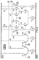
- the transfer terminals of the third, fifth and eighth transistors, T3, T5 and T8, are connected to a supply terminal VCC via a first resistor R1.
- the transfer terminals of the fourth, sixth and tenth transistors, T4, T6 and T10, are connected to said supply terminal VCC via a second resistor R2.
- the transfer terminals of the third and sixth transistors T3 and T6 form the output terminals S1 and S2 of the generation module GEN.
- the transfer terminals of the seventh and ninth transistors T7 and T9 are connected to the supply terminal VCC.
- the first, fourth and fifth differential pairs are polarized by first, fourth and fifth current sources I1, I4 and I5. These current sources will advantageously be configured so that they debit currents all having the same nominal value, denoted J.
- the signals Iout and Qout can respectively be expressed in the form REF + iout and REF + qout, where iout and qout are alternative components whose amplitude is small compared to the value of the reference signal REF.
- V (S1) -V (S2) J / 2. (Iout 2 -all 2 ) / (2.Vt) 2 ,
- This output signal is therefore proportional to the difference between the squares of the alternating components of the signals Iout and Qout, and is therefore representative of the difference between the squares of the amplitudes of said signals.
- This output signal V (S1) -V (S2) is applied to an input of the low-pass filter LPF, an output of which delivers the signal SP, which is therefore representative of a comparison between the powers conveyed by the signals Iout and Qout.
- the fourth and fifth differential pairs allow to subtract a part of the harmonic content that the output signal of a generation module would contain which would consist only of the first, second and third differential pairs.
- Such generation module would however deliver an output signal whose main component would be representative of the difference between the squares of the amplitudes of the signals Iout and Qout, but would have less spectral purity.
Landscapes
- Engineering & Computer Science (AREA)
- Power Engineering (AREA)
- Circuits Of Receivers In General (AREA)
- Digital Transmission Methods That Use Modulated Carrier Waves (AREA)
- Amplifiers (AREA)
- Control Of Amplification And Gain Control (AREA)
- Monitoring And Testing Of Transmission In General (AREA)
Applications Claiming Priority (2)
| Application Number | Priority Date | Filing Date | Title |
|---|---|---|---|
| FR9912066 | 1999-09-28 | ||
| FR9912066 | 1999-09-28 |
Publications (2)
| Publication Number | Publication Date |
|---|---|
| EP1089427A1 true EP1089427A1 (de) | 2001-04-04 |
| EP1089427B1 EP1089427B1 (de) | 2007-07-18 |
Family
ID=9550303
Family Applications (1)
| Application Number | Title | Priority Date | Filing Date |
|---|---|---|---|
| EP00203259A Expired - Lifetime EP1089427B1 (de) | 1999-09-28 | 2000-09-20 | Verfarhen zum Vergleichen der Amplituden von zwei elektrischen Signalen |
Country Status (6)
| Country | Link |
|---|---|
| US (1) | US6792254B1 (de) |
| EP (1) | EP1089427B1 (de) |
| JP (1) | JP2001168663A (de) |
| KR (1) | KR100744856B1 (de) |
| CN (1) | CN1227809C (de) |
| DE (1) | DE60035559T2 (de) |
Cited By (2)
| Publication number | Priority date | Publication date | Assignee | Title |
|---|---|---|---|---|
| WO2003005562A3 (en) * | 2001-07-02 | 2004-06-10 | Nokia Corp | Radio receiver using a feedback loop to compensate i/q amplitude errors, and method |
| EP1533909A1 (de) * | 2003-11-22 | 2005-05-25 | LG Electronics Inc. | Einrichtung und Verfahren zur Erhöhung der Empfangsrate eines Empfängers |
Families Citing this family (4)
| Publication number | Priority date | Publication date | Assignee | Title |
|---|---|---|---|---|
| US7433431B2 (en) * | 2003-09-12 | 2008-10-07 | Zarbana Digital Fund, Llc | Staggered AGC with digitally controlled VGA |
| CN101120567B (zh) * | 2005-01-11 | 2011-09-28 | 高通股份有限公司 | 生成用于两层QPSK turbo解码的比特LLR值的方法及相关UT、处理器 |
| KR100780192B1 (ko) * | 2006-09-29 | 2007-11-27 | 삼성전기주식회사 | 진폭 미스매칭을 개선한 주파수 변환장치 |
| JP5355936B2 (ja) * | 2007-06-28 | 2013-11-27 | 日本信号株式会社 | リーダライタ、及び物品仕分システム |
Citations (2)
| Publication number | Priority date | Publication date | Assignee | Title |
|---|---|---|---|---|
| US5287069A (en) * | 1990-02-07 | 1994-02-15 | Fujitsu Limited | Constant-amplitude wave combination type amplifier |
| US5446761A (en) * | 1993-06-11 | 1995-08-29 | Motorola, Inc. | Decoder circuit for phase modulated signals |
Family Cites Families (6)
| Publication number | Priority date | Publication date | Assignee | Title |
|---|---|---|---|---|
| EP0237590B1 (de) * | 1986-03-15 | 1989-08-09 | Deutsche ITT Industries GmbH | Regelschaltung zur Regelung von zwei ca. 90o Phasenverschiebung aufweisenden Signalen |
| EP0343273B1 (de) * | 1988-05-27 | 1994-04-27 | Deutsche ITT Industries GmbH | Korrekturschaltung für ein digitales Quadratur-Signalpaar |
| JP2982567B2 (ja) * | 1993-07-20 | 1999-11-22 | 松下電器産業株式会社 | 受信装置 |
| US5841889A (en) * | 1995-12-29 | 1998-11-24 | General Electric Company | Ultrasound image texture control using adaptive speckle control algorithm |
| KR0181377B1 (ko) * | 1996-08-30 | 1999-05-15 | 에스케이텔레콤주식회사 | 다수의 수신전력 검출기를 가지는 자동이득 제어장치 |
| CA2247555C (en) * | 1997-09-19 | 2001-12-11 | Samsung Electronics Co., Ltd. | Ntsc interference detectors using comb filters that suppress dtv pilot carrier to extract ntsc artifacts |
-
2000
- 2000-09-20 EP EP00203259A patent/EP1089427B1/de not_active Expired - Lifetime
- 2000-09-20 DE DE60035559T patent/DE60035559T2/de not_active Expired - Lifetime
- 2000-09-25 CN CNB001313827A patent/CN1227809C/zh not_active Expired - Fee Related
- 2000-09-27 US US09/671,128 patent/US6792254B1/en not_active Expired - Fee Related
- 2000-09-27 KR KR1020000056622A patent/KR100744856B1/ko not_active Expired - Fee Related
- 2000-09-28 JP JP2000296762A patent/JP2001168663A/ja not_active Withdrawn
Patent Citations (2)
| Publication number | Priority date | Publication date | Assignee | Title |
|---|---|---|---|---|
| US5287069A (en) * | 1990-02-07 | 1994-02-15 | Fujitsu Limited | Constant-amplitude wave combination type amplifier |
| US5446761A (en) * | 1993-06-11 | 1995-08-29 | Motorola, Inc. | Decoder circuit for phase modulated signals |
Cited By (3)
| Publication number | Priority date | Publication date | Assignee | Title |
|---|---|---|---|---|
| WO2003005562A3 (en) * | 2001-07-02 | 2004-06-10 | Nokia Corp | Radio receiver using a feedback loop to compensate i/q amplitude errors, and method |
| EP1533909A1 (de) * | 2003-11-22 | 2005-05-25 | LG Electronics Inc. | Einrichtung und Verfahren zur Erhöhung der Empfangsrate eines Empfängers |
| US7602865B2 (en) | 2003-11-22 | 2009-10-13 | Lg Electronics Inc. | Apparatus and method for enhancing a reception rate of a receiver |
Also Published As
| Publication number | Publication date |
|---|---|
| CN1227809C (zh) | 2005-11-16 |
| KR20010067235A (ko) | 2001-07-12 |
| EP1089427B1 (de) | 2007-07-18 |
| DE60035559D1 (de) | 2007-08-30 |
| KR100744856B1 (ko) | 2007-08-01 |
| CN1289930A (zh) | 2001-04-04 |
| DE60035559T2 (de) | 2008-08-14 |
| US6792254B1 (en) | 2004-09-14 |
| JP2001168663A (ja) | 2001-06-22 |
Similar Documents
| Publication | Publication Date | Title |
|---|---|---|
| EP3190711B1 (de) | Rf-empfänger mit frequenzverfolgung | |
| EP0624959B1 (de) | FM-Empfänger mit einer Schaltung zur Überabtastung | |
| EP1214780B1 (de) | Sender für funksignale, die mit einer autoadaptiven verstärkerspolarisation moduliert werden | |
| EP0071514B1 (de) | Einrichtung zur Rückgewinnung von Trägerwellen | |
| EP0530107B1 (de) | PSK-Demodulator mit Korrektur im Basisband für Phasen- oder Frequenzfehler | |
| FR2835120A1 (fr) | Procede et dispositif de preparation de signaux destines a etre compares pour etablir une pre-distorsion sur l'entree d'un amplificateur | |
| EP0929148A1 (de) | Verfahren und Vorrichtung zur numerischen Linearisierung eines Verstärkers | |
| FR2830704A1 (fr) | Emetteur a boucle polaire | |
| EP0600788A1 (de) | Analog-Digitalumsetzer | |
| WO2001076169A1 (fr) | Dispositif de production d'un signal radiofrequence module en phase et en amplitude | |
| EP0487386B1 (de) | Frequenzvervielfacher | |
| EP0798902A1 (de) | Robuster Phasenschätzer und Phasenrückgewinner für digitale Signale welche durch Phasenzittern betroffen sind | |
| EP1089427B1 (de) | Verfarhen zum Vergleichen der Amplituden von zwei elektrischen Signalen | |
| CN1135803C (zh) | 非相干6端口接收机 | |
| EP1039628B1 (de) | Hochintegrierter Hochfrequenzsender mit Beseitigung der Spiegelfrequenz, gegebenenfalls autokalibriert | |
| EP1441437B1 (de) | Betriebsfrequenzgesteuerte Quadratursignalgenerator | |
| FR2519818A1 (fr) | Boucle a blocage de phase et procede pour en ameliorer le signal de sortie | |
| EP1398873A1 (de) | Gilbert-Zellen-Mischer | |
| FR2809266A1 (fr) | Procede et dispositif de controle du dephasage entre quatre signaux mutuellement en quadrature de phase | |
| FR2837338A1 (fr) | Circuit de demodulation de porteuses en quadrature a haute efficacite | |
| FR2939579A1 (fr) | Circuit de conversion de frequence | |
| FR2785107A1 (fr) | Amplificateur de courant a faible impedance d'entree | |
| EP0473731B1 (de) | Verfahren und anordnung zum vergleich zweier veraenderlicher analogsignale | |
| FR2755808A1 (fr) | Estimateur d'un defaut de fonctionnement d'un modulateur en quadrature et etage de modulation l'utilisant | |
| EP0975126B1 (de) | Verfahren zur Schätzung des Frequenzfehlers in einem QPSK-Demodulator |
Legal Events
| Date | Code | Title | Description |
|---|---|---|---|
| PUAI | Public reference made under article 153(3) epc to a published international application that has entered the european phase |
Free format text: ORIGINAL CODE: 0009012 |
|
| AK | Designated contracting states |
Kind code of ref document: A1 Designated state(s): DE ES FR GB IT |
|
| AX | Request for extension of the european patent |
Free format text: AL;LT;LV;MK;RO;SI |
|
| 17P | Request for examination filed |
Effective date: 20011004 |
|
| AKX | Designation fees paid |
Free format text: DE ES FR GB IT |
|
| 17Q | First examination report despatched |
Effective date: 20050627 |
|
| GRAP | Despatch of communication of intention to grant a patent |
Free format text: ORIGINAL CODE: EPIDOSNIGR1 |
|
| GRAS | Grant fee paid |
Free format text: ORIGINAL CODE: EPIDOSNIGR3 |
|
| GRAA | (expected) grant |
Free format text: ORIGINAL CODE: 0009210 |
|
| AK | Designated contracting states |
Kind code of ref document: B1 Designated state(s): DE ES FR GB IT |
|
| REG | Reference to a national code |
Ref country code: GB Ref legal event code: FG4D Free format text: NOT ENGLISH |
|
| RAP2 | Party data changed (patent owner data changed or rights of a patent transferred) |
Owner name: NXP B.V. |
|
| REG | Reference to a national code |
Ref country code: GB Ref legal event code: ERR Free format text: NOTIFICATION HAS NOW BEEN RECEIVED FROM THE CORRECT NAME IS NXP B.V. THE CORRECTION WAS PUBLISHED IN THE EPO BULLETIN 07/31 DATED 20070801 |
|
| REF | Corresponds to: |
Ref document number: 60035559 Country of ref document: DE Date of ref document: 20070830 Kind code of ref document: P |
|
| GBT | Gb: translation of ep patent filed (gb section 77(6)(a)/1977) |
Effective date: 20071003 |
|
| PG25 | Lapsed in a contracting state [announced via postgrant information from national office to epo] |
Ref country code: ES Free format text: LAPSE BECAUSE OF FAILURE TO SUBMIT A TRANSLATION OF THE DESCRIPTION OR TO PAY THE FEE WITHIN THE PRESCRIBED TIME-LIMIT Effective date: 20071029 |
|
| PLBE | No opposition filed within time limit |
Free format text: ORIGINAL CODE: 0009261 |
|
| STAA | Information on the status of an ep patent application or granted ep patent |
Free format text: STATUS: NO OPPOSITION FILED WITHIN TIME LIMIT |
|
| 26N | No opposition filed |
Effective date: 20080421 |
|
| REG | Reference to a national code |
Ref country code: FR Ref legal event code: TP |
|
| PG25 | Lapsed in a contracting state [announced via postgrant information from national office to epo] |
Ref country code: IT Free format text: LAPSE BECAUSE OF NON-PAYMENT OF DUE FEES Effective date: 20070930 |
|
| REG | Reference to a national code |
Ref country code: FR Ref legal event code: PLFP Year of fee payment: 17 |
|
| REG | Reference to a national code |
Ref country code: FR Ref legal event code: PLFP Year of fee payment: 18 |
|
| REG | Reference to a national code |
Ref country code: FR Ref legal event code: PLFP Year of fee payment: 19 |
|
| PGFP | Annual fee paid to national office [announced via postgrant information from national office to epo] |
Ref country code: DE Payment date: 20180821 Year of fee payment: 19 Ref country code: FR Payment date: 20180822 Year of fee payment: 19 |
|
| PGFP | Annual fee paid to national office [announced via postgrant information from national office to epo] |
Ref country code: GB Payment date: 20180823 Year of fee payment: 19 |
|
| REG | Reference to a national code |
Ref country code: DE Ref legal event code: R119 Ref document number: 60035559 Country of ref document: DE |
|
| PG25 | Lapsed in a contracting state [announced via postgrant information from national office to epo] |
Ref country code: DE Free format text: LAPSE BECAUSE OF NON-PAYMENT OF DUE FEES Effective date: 20200401 |
|
| GBPC | Gb: european patent ceased through non-payment of renewal fee |
Effective date: 20190920 |
|
| PG25 | Lapsed in a contracting state [announced via postgrant information from national office to epo] |
Ref country code: GB Free format text: LAPSE BECAUSE OF NON-PAYMENT OF DUE FEES Effective date: 20190920 Ref country code: FR Free format text: LAPSE BECAUSE OF NON-PAYMENT OF DUE FEES Effective date: 20190930 |