EP1090415B1 - Dispositif a semi-conducteur avec contact ohmique et procede de realisation d'un contact sur un dispositif a semi-conducteur - Google Patents
Dispositif a semi-conducteur avec contact ohmique et procede de realisation d'un contact sur un dispositif a semi-conducteur Download PDFInfo
- Publication number
- EP1090415B1 EP1090415B1 EP99938136A EP99938136A EP1090415B1 EP 1090415 B1 EP1090415 B1 EP 1090415B1 EP 99938136 A EP99938136 A EP 99938136A EP 99938136 A EP99938136 A EP 99938136A EP 1090415 B1 EP1090415 B1 EP 1090415B1
- Authority
- EP
- European Patent Office
- Prior art keywords
- semiconductor
- contact
- regions
- region
- silicon carbide
- Prior art date
- Legal status (The legal status is an assumption and is not a legal conclusion. Google has not performed a legal analysis and makes no representation as to the accuracy of the status listed.)
- Expired - Lifetime
Links
Images


Classifications
-
- H—ELECTRICITY
- H10—SEMICONDUCTOR DEVICES; ELECTRIC SOLID-STATE DEVICES NOT OTHERWISE PROVIDED FOR
- H10D—INORGANIC ELECTRIC SEMICONDUCTOR DEVICES
- H10D64/00—Electrodes of devices having potential barriers
- H10D64/60—Electrodes characterised by their materials
- H10D64/62—Electrodes ohmically coupled to a semiconductor
-
- H—ELECTRICITY
- H10—SEMICONDUCTOR DEVICES; ELECTRIC SOLID-STATE DEVICES NOT OTHERWISE PROVIDED FOR
- H10D—INORGANIC ELECTRIC SEMICONDUCTOR DEVICES
- H10D64/00—Electrodes of devices having potential barriers
- H10D64/01—Manufacture or treatment
- H10D64/011—Manufacture or treatment of electrodes ohmically coupled to a semiconductor
- H10D64/0111—Manufacture or treatment of electrodes ohmically coupled to a semiconductor to Group IV semiconductors
- H10D64/0115—Manufacture or treatment of electrodes ohmically coupled to a semiconductor to Group IV semiconductors to silicon carbide
-
- Y—GENERAL TAGGING OF NEW TECHNOLOGICAL DEVELOPMENTS; GENERAL TAGGING OF CROSS-SECTIONAL TECHNOLOGIES SPANNING OVER SEVERAL SECTIONS OF THE IPC; TECHNICAL SUBJECTS COVERED BY FORMER USPC CROSS-REFERENCE ART COLLECTIONS [XRACs] AND DIGESTS
- Y10—TECHNICAL SUBJECTS COVERED BY FORMER USPC
- Y10S—TECHNICAL SUBJECTS COVERED BY FORMER USPC CROSS-REFERENCE ART COLLECTIONS [XRACs] AND DIGESTS
- Y10S438/00—Semiconductor device manufacturing: process
- Y10S438/931—Silicon carbide semiconductor
Definitions
- the invention relates to a semiconductor device with ohmic contacting and to a method for contacting a semiconductor device.
- the invention relates to such a semiconductor device which, at least in certain semiconductor regions, in particular the semiconductor regions which are contacted, consists of a predetermined polytype silicon carbide.
- Silicon carbide (SiC) in monocrystalline form is a semiconductor material with excellent physical properties, which make this semiconductor material interesting for power electronics even in applications in the kV range, due in part to its high breakdown field strength and good thermal conductivity.
- semiconductor silicon carbide power semiconductor devices such as Schottky diodes are also becoming increasingly popular.
- Other silicon carbide devices with increasing diffusion rate are pn diodes and transistors such as MOSFET (M etal O xide S emiconductor F ield E ffect T ransistors).
- n-type SiC accordingly takes place via a thin contact layer of a metal or via a layer sequence of different materials.
- the contact layers are tempered at temperatures between 600 ° C and 1100 ° C.
- transition metals such as nickel provide after the temperature treatment on n-type highly doped SiC a very good ohmic contact, since forms a metal silicide at temperatures of about 1000 ° C from the transition metal and the silicon contained in the SiC.
- Contact techniques for n-type SiC operating without a corresponding temperature treatment by comparison, provide a relatively high contact resistance or non-ohmic law current-voltage characteristic.
- the temperature treatment also has a positive effect on the temperature stability of the ohmic contacts formed.
- At least one covering layer of a material with a higher melting point such as, for example, nickel, tungsten, titanium or tantalum, is applied to the aluminum.
- MIS Metal Insulator Semiconductor
- a SiC semiconductor device whose ohmic contact consists of a titanium-aluminum alloy.
- the alloy serving as the contact electrode adheres particularly well to an n- or p-doped SiC layer when the aluminum content in the total weight of the alloy is in the range between 15% and 65%.
- the contacts on the n- and p-type semiconductor region in each case both have a low contact resistance and be temperature stable.
- only dopant concentrations should be provided for the n- and p-type SiC, which can be easily produced with currently available technologies.
- the invention is based on the finding that, contrary to the usual procedure of the art, is contacted in the n- and p-type silicon carbide ohmsch with each different material, a contacting of silicon carbide two conductivity type is still possible with a single material. This results in significant advantages in the production, since the need for a different contact material process steps omitted.
- the first and second semiconductor regions each have a sufficiently high dopant concentration at least on the surface of the semiconductor region. Therefore, the dopant concentrations are between 10 -17 cm -3 and 10 20 cm -3 . A particularly good contact is obtained when the dopant concentration is at least 10 19 cm -3 . This information applies to both the n- and the p-type line. These dopant concentrations can be easily generated, for example, by ion implantation.
- Decisive for the formation of a good ohmic contact resistance on both the n-type and p-type silicon carbide in this case is that the material is not applied in the form of a layer structure, but rather with a virtually homogeneous material composition on the respective semiconductor regions.
- composing the material from a plurality of material components is achieved by such a homogeneous material application, that at the interface to the two semiconductor regions each material component are directly present and can interact with the silicon carbide of the two semiconductor regions.
- mixing of the individual material components applied in the form of individual layers having a thickness of the order of a few nanometers is first necessary.
- the applied material contains a material component which acts as a donor or acceptor in silicon carbide
- this material component will migrate to some extent into the first or second semiconductor region, where it will be bound, for example, as a dopant at the corresponding lattice sites.
- This mixing process is significantly influenced by the original doping of the first or second semiconductor region and thus varies in the first and second boundary regions.
- the proportion of the relevant material component at least in the first and second limits, varies in a diverging, albeit very small, amount.
- the material contains a silicide-forming material component
- silicon originating in the first and second semiconductor regions mixes with the material of the first and second contact regions.
- a silicide based on the material component and the silicon are significant influencing factors, so that this effect can likewise lead to a slightly different material composition in the first and second boundary regions.
- the described interface effects do not have an effect, so that the material remains in its originally applied composition and thus resembles in these regions of the first and second contact regions.
- any minor differences in material composition of the first and second contact regions are not considered and subsumed under the terms "at least approximately the same material composition” and “practically homogeneous”.
- the applied material is composed of a first and second material component.
- the first material component consists of a material which forms an ohmic contact on n-type silicon carbide with a contact resistance of ⁇ 10 -1 ⁇ cm 2 , preferably ⁇ 10 -3 ⁇ cm 2
- the second material component contains an element of the third main group of the periodic table.
- the second material component is present in the material with a volume fraction of 0.1 to 50%. Preference is given to a proportion of 0.5 to 20%.
- the first material component is nickel and the second material component is aluminum, i.
- the material consists exclusively of nickel and aluminum. It is characterized by a good ohmic contact on the n-type semiconductor region due to the nickel.
- nickel content in the material also prevents the formation of liquid aluminum islands and the resulting undesirable evaporation of aluminum in the annealing process, which is advantageously carried out to form the ohmic contact.
- Particularly advantageous is an embodiment in which the first and second contact regions are produced simultaneously. This considerably reduces the number of process steps required compared to a successive application. Thus, shorter manufacturing cycles can be achieved.
- the material which is applied to the two semiconductor regions is taken from two separate sources.
- the sources each contain a material component, i. the first or the second.
- the removal takes place by simultaneous evaporation or sputtering (sputtering).
- the two contact regions are then formed by depositing the material components on the first and second semiconductor regions.
- the material for the two contact areas arises either still in the gas phase from the individual material components, in the course of the deposition process or only afterwards.
- An alternative embodiment provides, however, that from the first and second material component, a source material is first prepared, which is then atomized in a second process step.
- the leached particles of the material form the two contact regions on the n- and p-type silicon carbide.
- the first and second material components are applied alternately in thin layers to the two semiconductor regions. This can be done by sputtering from two separate sources, so that alternately in a short time sequence only one of the two material components from the associated source is atomized and deposited as a thin layer on the two semiconductor regions.
- the resulting thin layers have in particular only a thickness in the order of some ⁇ ngström. In the extreme case, such a thin layer may consist of only a single atomic layer, a so-called monolayer. Due to the small layer thickness and the short time sequence during the layer deposition, this material application of the two material components is also referred to as being simultaneous here.
- a mixing of the atoms of these monolayers then takes place, depending on the process conditions, at least partially during the application itself or at the very beginning of the subsequent annealing process. Due to the low layer thicknesses of this mixing process takes only a very short time.
- the semiconductor device after the two contact areas have been applied, subjected to a brief annealing process.
- the semiconductor arrangement is preferably heated to a maximum temperature of at least 500 ° C., in particular of approximately 1000 ° C., and then maintained at approximately this maximum temperature for up to 2 hours, in particular for 2 minutes.
- the tempering process can also consist of only one heating phase and an immediately following cooling phase without a residence time at a maximum temperature being provided therebetween. This process serves to form the two contact areas. It turns out that after this tempering process both on the first and on the second semiconductor region, ie on n- and p-conducting SiC, temperature-stable contacts with good ohmic characteristics and low contact resistance result.
- the first and second contact regions are arranged on a common layer surface or on different layer surfaces.
- the above-described training opportunities and advantages of contacting n- and p-type SiC with the same material apply in an analogous manner.
- embodiments are possible in which the two contact areas are formed contiguous or separate.
- the separation of the two contact areas can be carried out both during the application of the material by appropriate mask technique and then by removing too much applied material.
- common technologies such as e.g. the etching in question.
- the two semiconductor regions to be contacted may consist of SiC different polytypes. There are embodiments in which SiC in the form of 6H, 4H, 15R or 3C-SiC is used for the two semiconductor regions. Other polytypes are also possible.
- the semiconductor device may also consist of a material other than SiC. Therefore, in one embodiment, at least one further semiconductor region, for example a substrate, is made of a material other than SiC, for example silicon (Si), gallium arsenide (GaAs) or gallium nitride (GaN). This substrate is then integrated at least with the first and second semiconductor regions of SiC to form a hybrid semiconductor device.
- Si silicon
- GaAs gallium arsenide
- GaN gallium nitride
- the first and second contact regions are each located on a freely accessible surface of the semiconductor device.
- the first and second contact regions can also be covered by layers which are applied in the contacting of the following process steps.
- FIG. 1 a semiconductor device is shown in which a first contact region 110 and a second contact region 210 extend as a continuous layer over a first semiconductor region 100 and a second semiconductor region 200 adjacent thereto.
- the first and second semiconductor regions 100 and 200 are each made of 6H silicon carbide. They have a common layer surface 70, on which the first and second contact regions 110 and 210 are arranged.
- the first semiconductor region 100 is doped with a high proportion of donors, in the present case with nitrogen, and thus n-type.
- the second semiconductor region 200 has a high dopant concentration of aluminum.
- Aluminum is an acceptor in silicon carbide, so that the second semiconductor region is thus p-type.
- the donors and acceptors are introduced into the first and second semiconductor regions 100 and 200, respectively, by ion implantation.
- the dopant concentrations in the first and second semiconductor regions 100 and 200 are each 10 13 cm -3 . These high dopant concentrations are found in the FIG. 1 indicated by the symbols n + and p - .
- the first and second contact regions 110 and 210 are located on the first and second semiconductor regions 100 and 200.
- the two contact regions 110 and 210 consist of the same material, which is composed of a first and a second material component.
- the first material component is nickel, the second aluminum.
- the volume fraction is about 10%.
- the material for the first and second contact regions 110 and 210 is generated by evaporation from separate, not shown, nickel or aluminum sources. Subsequently, the formation of the first and second contact regions 110 and 210 takes place by depositing the gaseous material on the first and second semiconductor regions 100 and 200.
- the semiconductor device of FIG. 3 is used for forming and forming ohmic, temperature-stable contacts FIG. 1 then subjected to an approximately two-minute annealing process at about 1000 ° C.
- first semiconductor region 100 n-type
- first contact region 110 there is a contact resistance of less than 10 -4 ⁇ cm 2 and between the second semiconductor region 200 (p-type) and the second contact region 210 a contact resistance of less than 10 -3 ⁇ cm 2 .
- Boundary regions of the first and second contact regions 110 and 210 are identified by reference numerals 120 and 220, respectively.
- these boundary regions 120 and 220 due to exchanges between the first semiconductor region 100 and the first contact region 110 arise and the second semiconductor region 200 and the second contact region 210, slight changes in the composition of the material originally deposited in the first and second contact regions 110 and 210. Apart from the resulting slight differences in the material composition of the first and second boundary regions 120 and 220, the first and second contact regions 110 and 210 have the same material composition. It is also possible that the boundary regions 120 and 220, in which the said exchanges take place, also extend into the semiconductor regions 100 and 200, respectively. In FIG. 1 However, this case is not shown.
- FIG. 2 shows a semiconductor device in a layer sequence with the first contact region 110 as the bottom layer, the second contact region 210 as the top layer and a plurality of intervening SiC layers.
- the first and second contact regions 110 and 210 in turn have the first and second boundary regions 120 and 220 adjoining the respective adjacent SiC layer.
- the sub-stack of the SiC layers is composed in ascending order of the first semiconductor region 100, an n - SiC layer 3, a p-type SiC layer 11 and the second semiconductor region 200.
- the first contact region 110 is arranged on a first layer surface 71 of the first semiconductor region 100, which at the same time also forms a lower main surface of the sub-stack of the SiC layers.
- the second contact region 210 is arranged on a second layer surface 72 of the second semiconductor region 200, which at the same time forms an upper main surface of the sub-stack of the SiC layers.
- the first semiconductor region 100 which in the exemplary embodiment of FIG. 2 may also represent a SiC substrate 100a again has a high n-type conductivity, the second semiconductor region 200, however, a high p-type conductivity.
- the first and second semiconductor regions 100 and 200 as well as in the first and second contact regions 110 and 210 provided materials and dopants correspond to those of the embodiment of FIG. 1 , This analogy also applies to the method for applying the first and second contact regions 110 and 210.
- the semiconductor device of FIG. 2 has between the n - SiC layer 3 and the p-layer 11 has a pn junction 17, which essentially determines the function of this semiconductor device.
- a pn junction 17 may be both part of a larger circuit arrangement, as well as represent a separate component in the form of a pn diode. In both cases, an ohmic contacting of semiconductor regions of different conductivity type via the contact regions 110 and 210 is necessary.
- the illustrated embodiment is an example of a semiconductor device having first and second contact regions 110 and 210 on different layer surfaces 71 and 72 of the semiconductor device.
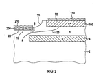
- FIG. 3 1 a semiconductor device is shown in which the first and the second contact regions 110 and 210 are arranged on the common layer surface 70 of the semiconductor device, but in contrast to the exemplary embodiment of FIG. 1 are spatially separated from each other.
- the function of the semiconductor device of FIG. 3 consists of controlling a current flow 50, which emanates from the first semiconductor region 100 or from the first contact region 110 and which passes through an n-SiC layer 2, within a channel region 8 of this n-SiC layer 2.
- the channel region 8 can be changed in its dimensions and thus in its resistance by the second semiconductor region 200 and a p-island 4 buried in the n-SiC layer 2. This is done by applying a voltage to the second contact region 210, whereby a depletion zone 20 at a Pn junction 19 between the n-type SiC layer 2 and the p-type second semiconductor region 200 among others in the channel region 8 into propagates.
- the dimension of the channel region 8 is additionally preset by providing a depression 30 in which the second semiconductor region 200 is located.
- Both the n-type first semiconductor region 100 and the p-type second semiconductor region 200 require an ohmic contact in the form of the first and second contact regions 110 and 210 for the described mode of operation.
- the first semiconductor region 100 has an n-doping with the donor phosphor, the second semiconductor region 200 a p-doping with the acceptor boron.
- the dopant concentration is in each case 10 19 cm -3 .
- a material for the first and the second contact region 110 and 210 is used in the example of FIG. 3 , which does not fall under the invention, a material mixture composed of the first material component tungsten and the second material component gallium.
- the volume fraction of gallium is about 5%.
- FIG. 4 shows a semiconductor device in the form of a vertical MOSFET based on silicon carbide.
- the MOSFET includes a plurality of first and second semiconductor regions 100 and 200.
- the in the Figures 1 and 2 shown semiconductor devices can be found in the MOSFET of FIG. 4 as substructures again. They are identified by a dashed circle or a dashed rectangle.
- the vertical MOSFET of FIG. 4 is mirror-symmetric with respect to a plane of symmetry 60.
- the lowest lying first semiconductor region 100 is also associated with FIG FIG. 4 as substrate 100a.
- the n - SiC layer 3 is arranged on one of which perpendicular to Symmetry plane 60 directed surface 40.
- the n - SiC layer 3 is arranged on one of which perpendicular to Symmetry plane 60 directed surface 40.
- the n - SiC layer 3 is arranged.
- 42 includes two separate, with respect to the plane of symmetry at a side facing away from the SiC substrate 100 a surface 60 arranged mirror-symmetrically p-layers 11, these include in turn each first and second semiconductor regions 100 and 200 which adjoin one another ,
- the first and second semiconductor regions 100 and 200 are electrically contacted by the first and second contact regions 110 and 210 associated therewith.
- the contiguous first and second contact regions 110 and 210 may be in the in FIG. 4 also be regarded as a source electrode 110a.
- a further first contact region 110 On one of the n - SiC layer 3 facing away from surface 41 of SiC substrate 100a, there is a further first contact region 110, which may be considered herein as a drain electrode 110b.
- the operation of the vertical MOSFETs of FIG. 4 to control the current flow 50 between the drain 110b and the source 110a runs through a vertical drift region 9 in the SiC substrate 100a and in the n - SiC layer 3, and a lateral channel region 80 in the p-layer 11.
- the resistance of the channel region 80 can be adjusted by a gate electrode 14 wherein an electrically insulating oxide layer 13 separates the gate electrode 14 from the channel region 80 in the p-layer 11.
- first and second semiconductor regions 100 and 200 with different conduction types is frequently required.
- the contacting takes place as in the examples of FIGS. 1 to 3 already described.
- semiconductor devices part of a complex semiconductor device, which consequently includes a plurality of first and second semiconductor regions 100 and 200 together with the contacting via the associated first and second contact regions 110 and 210.
Landscapes
- Electrodes Of Semiconductors (AREA)
Abstract
Claims (13)
- Dispositif à semi-conducteur avec contact ohmique, ledit dispositif à semi-conducteur comprenant :a) au moins une première région semi-conductrice (100), constituée de carbure de silicium de type n,b) au moins une seconde région semi-conductrice (200), constituée de carbure de silicium de type p, les concentrations de dopant du carbure de silicium de type n et du carbure de silicium de type p étant chacune comprises entre 1017cm-3 et 1020 cm-3,c) au moins une première région de contact (110), adjacente à la première région semi-conductrice (100), etd) au moins une seconde région de contact (210), adjacente à la seconde région semi-conductrice (200),e) la première et la seconde région de contact (110, 210) réalisant chacune un contact ohmique et étant constituées du même matériau pratiquement homogène et contenant exclusivement du nickel et de l'aluminium, la fraction volumique de l'aluminium étant comprise entre 0,1 % et 50 %.
- Dispositif à semi-conducteur selon la revendication 1, caractérisé en ce que la première et la seconde région de contact (110, 210) sont disposées sur une surface de couche commune (70).
- Dispositif à semi-conducteur selon la revendication 1, caractérisé en ce que la première et la seconde région de contact (110, 210) sont disposées sur des surfaces de couches différentes (71, 72).
- Dispositif à semi-conducteur selon la revendication 1 ou 2, caractérisé en ce que la première et la seconde région de contact (110, 210) sont conçues de manière contigüe.
- Dispositif à semi-conducteur selon l'une des revendications 1 à 3, caractérisé en ce que la première et la seconde région de contact (110, 210) sont conçues de manière séparée.
- Dispositif à semi-conducteur selon l'une des revendications 1 à 5, caractérisé en ce que la fraction volumique de l'aluminium est comprise entre 0,5 % et 20 %.
- Procédé de réalisation d'un contact ohmique sur un dispositif à semi-conducteur, dans lequel
il est créé une première région de contact (110) sur une première région semi-conductrice (100) constituée de carbure de silicium de type n et ayant une concentration de dopant comprise entre 1017 cm-3 et 1020 cm-3, et une seconde région de contact (210) sur une seconde région semi-conductrice (200) constituée de carbure de silicium de type p et ayant une concentration de dopant comprise entre 1017 cm-3 et 1020 cm-3, en déposant le même matériau pratiquement homogène et contenant exclusivement du nickel et de l'aluminium, de telle manière que la fraction volumique de l'aluminium soit comprise entre 0,1 % et 50 %. - Procédé selon la revendication 7, caractérisé en ce que la première et la seconde région de contact (110, 210) sont déposées simultanément sur la première et la seconde région semi-conductrice (100, 200).
- Procédé selon la revendication 7 ou 8, caractérisé en ce que la fraction volumique de l'aluminium dans le matériau déposé est comprise entre 0,5 % et 20 %.
- Procédé selon l'une des revendications 7 à 9, caractérisé en ce que le matériau est déposé par vaporisation ou pulvérisation simultanée à partir d'une source de nickel et une source d'aluminium.
- Procédé selon l'une des revendications 7 à 9, caractérisé en ce qu'une source contenant du nickel et de l'aluminium est d'abord fabriquée, puis le matériau est déposé par pulvérisation du matériau source.
- Procédé selon l'une des revendications 7 à 11, caractérisé en ce que le dispositif à semi-conducteur, comprenant la première et la seconde région semi-conductrices (100, 200) ainsi que la première et la seconde région de contact déposées (110, 210), est soumis à un processus de recuit avec un chauffage jusqu'à une température maximale au moins égale à 500°C, de préférence de l'ordre de 1000°C.
- Procédé selon la revendication 12, caractérisé en ce que la température maximale est maintenue constante pendant une durée comprise entre 2 minutes tout au plus et 2 heures tout au plus.
Applications Claiming Priority (3)
| Application Number | Priority Date | Filing Date | Title |
|---|---|---|---|
| DE19825519 | 1998-06-08 | ||
| DE19825519 | 1998-06-08 | ||
| PCT/DE1999/001659 WO1999065067A1 (fr) | 1998-06-08 | 1999-06-07 | Dispositif a semi-conducteur avec contact ohmique et procede de realisation d'un contact sur un dispositif a semi-conducteur |
Publications (2)
| Publication Number | Publication Date |
|---|---|
| EP1090415A1 EP1090415A1 (fr) | 2001-04-11 |
| EP1090415B1 true EP1090415B1 (fr) | 2010-11-17 |
Family
ID=7870259
Family Applications (1)
| Application Number | Title | Priority Date | Filing Date |
|---|---|---|---|
| EP99938136A Expired - Lifetime EP1090415B1 (fr) | 1998-06-08 | 1999-06-07 | Dispositif a semi-conducteur avec contact ohmique et procede de realisation d'un contact sur un dispositif a semi-conducteur |
Country Status (4)
| Country | Link |
|---|---|
| US (1) | US6667495B2 (fr) |
| EP (1) | EP1090415B1 (fr) |
| DE (2) | DE19925233A1 (fr) |
| WO (1) | WO1999065067A1 (fr) |
Families Citing this family (11)
| Publication number | Priority date | Publication date | Assignee | Title |
|---|---|---|---|---|
| US20040120371A1 (en) * | 2000-02-18 | 2004-06-24 | Jds Uniphase Corporation | Contact structure for a semiconductor component |
| DE10036208B4 (de) * | 2000-07-25 | 2007-04-19 | Siced Electronics Development Gmbh & Co. Kg | Halbleiteraufbau mit vergrabenem Inselgebiet und Konaktgebiet |
| DE10051049B4 (de) * | 2000-10-14 | 2011-04-07 | Cree, Inc. | Aluminium-Nickel-Kontaktmetallisierung für p-dotiertes SiC und Herstellungsverfahren dafür |
| JP2003173673A (ja) * | 2001-11-30 | 2003-06-20 | Sanyo Electric Co Ltd | 強誘電体メモリ |
| US7138291B2 (en) * | 2003-01-30 | 2006-11-21 | Cree, Inc. | Methods of treating a silicon carbide substrate for improved epitaxial deposition and resulting structures and devices |
| JP4122880B2 (ja) * | 2002-07-24 | 2008-07-23 | 住友電気工業株式会社 | 縦型接合型電界効果トランジスタ |
| ATE536635T1 (de) * | 2004-07-08 | 2011-12-15 | Semisouth Lab Inc | Monolithischer vertikal- sperrschichtfeldeffekttransistor und aus siliziumcarbid hergestellte schottky- barrierendiode und herstellungsverfahren dafür |
| DE112006002377B4 (de) * | 2005-09-08 | 2014-04-24 | Mitsubishi Denki K.K. | Halbleitervorrichtung und Verfahren zum Herstellen einer Halbleitervorrichtung |
| US7829374B2 (en) * | 2007-07-20 | 2010-11-09 | Panasonic Corporation | Silicon carbide semiconductor device and method for manufacturing the same |
| JP4858791B2 (ja) * | 2009-05-22 | 2012-01-18 | 住友電気工業株式会社 | 半導体装置およびその製造方法 |
| US9466698B2 (en) * | 2013-03-15 | 2016-10-11 | Semiconductor Components Industries, Llc | Electronic device including vertical conductive regions and a process of forming the same |
Family Cites Families (17)
| Publication number | Priority date | Publication date | Assignee | Title |
|---|---|---|---|---|
| US3662458A (en) * | 1969-06-20 | 1972-05-16 | Westinghouse Electric Corp | Electrical contact for silicon carbide members |
| US3982262A (en) * | 1974-04-17 | 1976-09-21 | Karatsjuba Anatoly Prokofievic | Semiconductor indicating instrument |
| US4320251A (en) * | 1980-07-28 | 1982-03-16 | Solamat Inc. | Ohmic contacts for solar cells by arc plasma spraying |
| US5027168A (en) * | 1988-12-14 | 1991-06-25 | Cree Research, Inc. | Blue light emitting diode formed in silicon carbide |
| US4918497A (en) * | 1988-12-14 | 1990-04-17 | Cree Research, Inc. | Blue light emitting diode formed in silicon carbide |
| JP2509713B2 (ja) * | 1989-10-18 | 1996-06-26 | シャープ株式会社 | 炭化珪素半導体装置およびその製造方法 |
| US5281831A (en) * | 1990-10-31 | 1994-01-25 | Kabushiki Kaisha Toshiba | Optical semiconductor device |
| US5264713A (en) * | 1991-06-14 | 1993-11-23 | Cree Research, Inc. | Junction field-effect transistor formed in silicon carbide |
| US5465249A (en) * | 1991-11-26 | 1995-11-07 | Cree Research, Inc. | Nonvolatile random access memory device having transistor and capacitor made in silicon carbide substrate |
| US5539217A (en) * | 1993-08-09 | 1996-07-23 | Cree Research, Inc. | Silicon carbide thyristor |
| WO1995024055A1 (fr) * | 1994-03-04 | 1995-09-08 | Siemens Aktiengesellschaft | Structure mis a base de carbure de silicium a resistance elevee au verrouillage |
| US5449925A (en) * | 1994-05-04 | 1995-09-12 | North Carolina State University | Voltage breakdown resistant monocrystalline silicon carbide semiconductor devices |
| US5523589A (en) * | 1994-09-20 | 1996-06-04 | Cree Research, Inc. | Vertical geometry light emitting diode with group III nitride active layer and extended lifetime |
| JPH0897441A (ja) * | 1994-09-26 | 1996-04-12 | Fuji Electric Co Ltd | 炭化けい素ショットキーダイオードの製造方法 |
| US5929523A (en) * | 1996-03-07 | 1999-07-27 | 3C Semiconductor Corporation | Os rectifying Schottky and ohmic junction and W/WC/TiC ohmic contacts on SiC |
| US6180958B1 (en) * | 1997-02-07 | 2001-01-30 | James Albert Cooper, Jr. | Structure for increasing the maximum voltage of silicon carbide power transistors |
| US6011278A (en) * | 1997-10-28 | 2000-01-04 | Philips Electronics North America Corporation | Lateral silicon carbide semiconductor device having a drift region with a varying doping level |
-
1999
- 1999-06-01 DE DE19925233A patent/DE19925233A1/de not_active Withdrawn
- 1999-06-07 WO PCT/DE1999/001659 patent/WO1999065067A1/fr not_active Ceased
- 1999-06-07 DE DE59915222T patent/DE59915222D1/de not_active Expired - Lifetime
- 1999-06-07 EP EP99938136A patent/EP1090415B1/fr not_active Expired - Lifetime
-
2000
- 2000-12-08 US US09/732,989 patent/US6667495B2/en not_active Expired - Lifetime
Also Published As
| Publication number | Publication date |
|---|---|
| WO1999065067A1 (fr) | 1999-12-16 |
| DE59915222D1 (de) | 2010-12-30 |
| EP1090415A1 (fr) | 2001-04-11 |
| DE19925233A1 (de) | 1999-12-09 |
| US6667495B2 (en) | 2003-12-23 |
| US20010001484A1 (en) | 2001-05-24 |
Similar Documents
| Publication | Publication Date | Title |
|---|---|---|
| EP1222694B1 (fr) | Dispositif semi-conducteur en SiC à contact Schottky et sa méthode de fabrication | |
| DE69126901T2 (de) | Halbleiteranordnungen aus Diamant | |
| DE112015004093B4 (de) | Siliciumcarbid-halbleitervorrichtung und verfahren zum herstellen einer siliciumcarbid-halbleitervorrichtung | |
| DE60031173T2 (de) | Misfet | |
| DE69127314T2 (de) | Diamant-Halbleiteranordnung | |
| DE3141967C2 (fr) | ||
| DE102015103070B4 (de) | Leistungshalbleitervorrichtung mit trenchgatestrukturen mit zu einer hauptkristallrichtung geneigten längsachsen und herstellungsverfahren | |
| DE69511726T2 (de) | Halbleiteranordnung mit isoliertem gate | |
| DE112018003362T5 (de) | Oxid-halbleitereinheit und verfahren zur herstellung einer oxid-halbleitereinheit | |
| DE102009033302B4 (de) | Herstellungsverfahren für ein unipolares Halbleiter-Bauelement und Halbleitervorrichtung | |
| DE112019003790T5 (de) | Superjunction-siliziumkarbid-halbleitervorrichtung und verfahren zum herstellen einer superjunction-siliziumkarbid-halbleitervorrichtung | |
| DE112017007060T5 (de) | Leistungshalbleitereinheit | |
| DE3811821A1 (de) | Halbleiterbauelement | |
| DE10025264A1 (de) | Feldeffekt-Transistor auf der Basis von eingebetteten Clusterstrukturen und Verfahren zu seiner Herstellung | |
| DE2455730B2 (de) | Feldeffekt-Transistor | |
| DE4025269A1 (de) | Elektronisches bauelement und verfahren zu dessen herstellung | |
| DE10229146A1 (de) | Laterales Superjunction-Halbleiterbauteil | |
| DE2805442A1 (de) | Verfahren zum herstellen eines schottky-sperrschicht-halbleiterbauelementes | |
| DE112016006723T5 (de) | Halbleitereinrichtung | |
| EP1090415B1 (fr) | Dispositif a semi-conducteur avec contact ohmique et procede de realisation d'un contact sur un dispositif a semi-conducteur | |
| EP1114465B1 (fr) | Dispositif a semiconducteur a contact ohmique et procede pour etablir un contact ohmique avec un tel dispositif | |
| DE60028727T2 (de) | Herstellungsverfahren für Bauelemente mit gradiertem Top-Oxid und Drift-Gebiet | |
| DE102007009227A1 (de) | Halbleiterbauelement mit gleichrichtenden Übergängen sowie Herstellungsverfahren zur Herstellung desselben | |
| DE60030059T2 (de) | Durchbruchsdiode und verfahren zur herstellung | |
| WO2000038246A1 (fr) | Transistor a effet de champ dote d'une couche d'appauvrissement et d'une zone de connexion hautement dopee |
Legal Events
| Date | Code | Title | Description |
|---|---|---|---|
| PUAI | Public reference made under article 153(3) epc to a published international application that has entered the european phase |
Free format text: ORIGINAL CODE: 0009012 |
|
| 17P | Request for examination filed |
Effective date: 20001103 |
|
| AK | Designated contracting states |
Kind code of ref document: A1 Designated state(s): CH DE FR IT LI SE |
|
| 17Q | First examination report despatched |
Effective date: 20080401 |
|
| GRAP | Despatch of communication of intention to grant a patent |
Free format text: ORIGINAL CODE: EPIDOSNIGR1 |
|
| RIN1 | Information on inventor provided before grant (corrected) |
Inventor name: SCHOERNER, REINHOLD Inventor name: PETERS, DETHARD Inventor name: FRIEDRICHS, PETER |
|
| GRAS | Grant fee paid |
Free format text: ORIGINAL CODE: EPIDOSNIGR3 |
|
| GRAA | (expected) grant |
Free format text: ORIGINAL CODE: 0009210 |
|
| AK | Designated contracting states |
Kind code of ref document: B1 Designated state(s): CH DE FR IT LI SE |
|
| REG | Reference to a national code |
Ref country code: CH Ref legal event code: EP |
|
| REF | Corresponds to: |
Ref document number: 59915222 Country of ref document: DE Date of ref document: 20101230 Kind code of ref document: P |
|
| RAP2 | Party data changed (patent owner data changed or rights of a patent transferred) |
Owner name: INFINEON TECHNOLOGIES AG |
|
| REG | Reference to a national code |
Ref country code: FR Ref legal event code: TP |
|
| PG25 | Lapsed in a contracting state [announced via postgrant information from national office to epo] |
Ref country code: SE Free format text: LAPSE BECAUSE OF FAILURE TO SUBMIT A TRANSLATION OF THE DESCRIPTION OR TO PAY THE FEE WITHIN THE PRESCRIBED TIME-LIMIT Effective date: 20101117 |
|
| PLBE | No opposition filed within time limit |
Free format text: ORIGINAL CODE: 0009261 |
|
| STAA | Information on the status of an ep patent application or granted ep patent |
Free format text: STATUS: NO OPPOSITION FILED WITHIN TIME LIMIT |
|
| 26N | No opposition filed |
Effective date: 20110818 |
|
| REG | Reference to a national code |
Ref country code: DE Ref legal event code: R097 Ref document number: 59915222 Country of ref document: DE Effective date: 20110818 |
|
| PG25 | Lapsed in a contracting state [announced via postgrant information from national office to epo] |
Ref country code: IT Free format text: LAPSE BECAUSE OF FAILURE TO SUBMIT A TRANSLATION OF THE DESCRIPTION OR TO PAY THE FEE WITHIN THE PRESCRIBED TIME-LIMIT Effective date: 20101117 |
|
| REG | Reference to a national code |
Ref country code: CH Ref legal event code: PL |
|
| PG25 | Lapsed in a contracting state [announced via postgrant information from national office to epo] |
Ref country code: LI Free format text: LAPSE BECAUSE OF NON-PAYMENT OF DUE FEES Effective date: 20110630 Ref country code: CH Free format text: LAPSE BECAUSE OF NON-PAYMENT OF DUE FEES Effective date: 20110630 |
|
| PGFP | Annual fee paid to national office [announced via postgrant information from national office to epo] |
Ref country code: DE Payment date: 20140814 Year of fee payment: 16 |
|
| PGFP | Annual fee paid to national office [announced via postgrant information from national office to epo] |
Ref country code: FR Payment date: 20140619 Year of fee payment: 16 |
|
| REG | Reference to a national code |
Ref country code: DE Ref legal event code: R119 Ref document number: 59915222 Country of ref document: DE |
|
| REG | Reference to a national code |
Ref country code: FR Ref legal event code: ST Effective date: 20160229 |
|
| PG25 | Lapsed in a contracting state [announced via postgrant information from national office to epo] |
Ref country code: DE Free format text: LAPSE BECAUSE OF NON-PAYMENT OF DUE FEES Effective date: 20160101 |
|
| PG25 | Lapsed in a contracting state [announced via postgrant information from national office to epo] |
Ref country code: FR Free format text: LAPSE BECAUSE OF NON-PAYMENT OF DUE FEES Effective date: 20150630 |