EP1090460B1 - Circuit de reinitialisation - Google Patents
Circuit de reinitialisation Download PDFInfo
- Publication number
- EP1090460B1 EP1090460B1 EP99938180A EP99938180A EP1090460B1 EP 1090460 B1 EP1090460 B1 EP 1090460B1 EP 99938180 A EP99938180 A EP 99938180A EP 99938180 A EP99938180 A EP 99938180A EP 1090460 B1 EP1090460 B1 EP 1090460B1
- Authority
- EP
- European Patent Office
- Prior art keywords
- supply voltage
- circuit
- current source
- reset circuit
- reset
- Prior art date
- Legal status (The legal status is an assumption and is not a legal conclusion. Google has not performed a legal analysis and makes no representation as to the accuracy of the status listed.)
- Expired - Lifetime
Links
Images

Classifications
-
- G—PHYSICS
- G06—COMPUTING OR CALCULATING; COUNTING
- G06F—ELECTRIC DIGITAL DATA PROCESSING
- G06F1/00—Details not covered by groups G06F3/00 - G06F13/00 and G06F21/00
- G06F1/24—Resetting means
-
- G—PHYSICS
- G06—COMPUTING OR CALCULATING; COUNTING
- G06F—ELECTRIC DIGITAL DATA PROCESSING
- G06F1/00—Details not covered by groups G06F3/00 - G06F13/00 and G06F21/00
- G06F1/26—Power supply means, e.g. regulation thereof
- G06F1/30—Means for acting in the event of power-supply failure or interruption, e.g. power-supply fluctuations
-
- Y—GENERAL TAGGING OF NEW TECHNOLOGICAL DEVELOPMENTS; GENERAL TAGGING OF CROSS-SECTIONAL TECHNOLOGIES SPANNING OVER SEVERAL SECTIONS OF THE IPC; TECHNICAL SUBJECTS COVERED BY FORMER USPC CROSS-REFERENCE ART COLLECTIONS [XRACs] AND DIGESTS
- Y10—TECHNICAL SUBJECTS COVERED BY FORMER USPC
- Y10S—TECHNICAL SUBJECTS COVERED BY FORMER USPC CROSS-REFERENCE ART COLLECTIONS [XRACs] AND DIGESTS
- Y10S323/00—Electricity: power supply or regulation systems
- Y10S323/901—Starting circuits
Definitions
- the invention relates to a reset circuit according to the preamble of claim 1.
- a reset circuit of the generic type is used for deactivation an external circuit configuration, for example in the form of a Microcontroller circuit by a supply voltage is operated and in a stable, deactivated state should be brought when the supply voltage one falls below a certain level, so that logic circuits in connection with the microcontroller circuit no undefined States can assume the external circuit configuration is deactivated.
- Prior art reset circuits operate e.g. With one powered by the supply voltage of the microcontroller Charge pump and a transistor as an actuator which drops a bias voltage, which in the charge pump Normal operation can be kept very small and that with undervoltage supply takes on a relatively large value and thus the microcontroller circuit from a certain supply voltage sure disabled. This results in a Hysteresis effect, so that the microcontroller circuit only "starts up” again when the supply voltage exceeds a certain level Threshold increases.
- Circuits of the aforementioned type are relatively complex and inexpensive.
- DE 195 27 603 A1 describes an electrical circuit arrangement to generate a reset signal for undervoltage supply of a microcomputer known, which one to be monitored Voltage series connection of an npn transistor and has a resistor at their connection point the reset signal can be tapped.
- the resistance must be relative be high impedance to the thermal load of the transistor to keep within limits. This resistance forms together with in the microcomputer, with the positive pole of the monitoring voltage connected resistors a voltage divider, whereby a clear reset signal (low signal) is not guaranteed.
- EP 0 767 416 A1 discloses a circuit for voltage supply of a microcomputer with generation of a reset signal with undervoltage supply, which has several capacitors having. In the time between falling below the Minimum supply voltage and the appearance of a reset signal undefined states can arise, which under should be avoided in all circumstances.
- the present invention is therefore based on the object a reset circuit for an external circuit configuration specify that over a wide supply voltage range works reliably with just a few components and is therefore inexpensive and easy to integrate.
- the reset circuit according to the invention has the advantage that only a minimum of components is needed and disable that the external circuit configuration is done reliably.
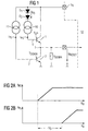
- the reset circuit shows with the reference numerals 1 and 2 two between supply voltage Uv and Ground reference potential with its passages connected in series active switching elements.
- the reset signal Ureset is active as a low signal to deactivate
- an external microcontroller circuit 12 The connection point 5 is via the resistor Rdown with ground reference potential connected.
- the resistance Rdown can also be omitted.
- the active switching elements 1 and 2 it is bipolar npn transistors in the embodiment Tup and Tdown.
- the bases as control connections 6.7 of the active switching elements 1.2 in the form of the bipolar Transistors Tup and Tdown are directly connected to each one of the Supply voltage Uv fed current source 10 and 11 with driven by the currents IPU or IPD.
- One power source 10 is via at least one diode D1 polarized in the forward direction connected to the supply voltage Uv. In the preferred Embodiment of Fig. 1 are between power source 10 and Supply voltage Uv two or more polarized in the forward direction Diodes D1, D2 are provided.
- the mode of operation of the first exemplary embodiment shown in FIG. 1 be based on the diagrams of FIGS. 2a and 2b explained.
- the supply voltage Uv one to operate the external Circuit configuration 12 for example in the form of a microcontroller has a sufficiently high level of, for example, 5V
- the currents IPU and IPD flow to control the respective active switching element 1 and 2 in the form of bipolar npn transistors Tup or Tdown and it stands at the connection point 5 due to the selected currents IPU and IPD and due to the characteristic curve of the two bipolar Transistors Tup or Tdown a high level.
- the external Circuit configuration 12 is not deactivated thereby but remains in its operating state.
- the microcontroller circuit 12 is thereby deactivated.
- Each power source requires a certain drop voltage to operate.
- By inserting the two diodes D1 and D2 becomes the available voltage for the transistor Tup driving power source IPU reduced. To this In this way it can be ensured that when the supply voltage drops Uv first the current drops IPU and only then the current IPD, which drives the transistor Tdown.
- the pass line of the transistor Tdown is therefore even lower Supply voltage Uv kept low than that of Transistor tup. Therefore, the reset signal Ureset with falling Supply voltage Uv in any case to a low level drawn. If the supply voltage Uv is so low that the current IPD of the current source 11 to a halt comes, the resistor Rdown takes over the task, the reset signal Keep ureset defined at a low level.
- the active switching elements are one made of field effect transistors 3,4 formed current mirror circuit 9 and a bipolar Transistor provided.
- the from the field effect transistor 4 on the Field effect transistor 3 mirrored current is designated IUP and that through the collector-emitter path of the bipolar Transistor 2 flowing current with IPD. It is about the currents IUP and IPD by the current amplification factor of the transistors increased current of the current source 10 and 11.
- the gate electrode 8 of both field effect transistors 3, 4 is with the current source 10 and with the drain electrode of the field effect transistor 4 connected.
- FIGS. 4a and 4b are basically identical to FIGS. 2a, b. Only the difference is shown in FIGS. 4a, b that the threshold voltage of the field effect transistors, which is additionally approximately 2 V, is superimposed on the diode forward voltages Ud of the two diodes D1 and D2 as a gate-source voltage. Therefore, the diodes D1 and D2 can also be omitted when using the current mirror circuit with the field effect transistors.
- the current mirror circuit 9 is characterized in that the one field effect transistor 3 with its drain-source path between supply voltage Uv and the connection point 5 lies and the other field effect transistor 4 with its Drain-source path between a current source 10 and Ground reference potential.
- the gate electrodes 8 of both field effect transistors 3,4 are interconnected and with one Power source 10 connected.
- the reset signal Ureset is an active low signal.
- FIGS. 1 and 3 can also as a supplement to a comparator circuit (not shown) are used. By such a comparator circuit the accuracy of the reset threshold is significantly increased.
- the circuits described provide a safe reset signal Ureset even if the minimum operating voltage is undershot of the comparator guaranteed.
- the reset circuit according to the invention is characterized by use in automotive electronics.
Landscapes
- Engineering & Computer Science (AREA)
- Theoretical Computer Science (AREA)
- Physics & Mathematics (AREA)
- General Engineering & Computer Science (AREA)
- General Physics & Mathematics (AREA)
- Electronic Switches (AREA)
Claims (5)
- Circuit de remise à l'état initial pour désactiver une configuration de circuit (12) alimentée par une tension d'alimentation (Uv), dans le cas d'une alimentation avec une tension trop faible,qui est constitué de deux éléments de commutation actifs (1-2; 4; 3-2), branchés en série, avec leurs trajets de conduction, entre la tension d'alimentation (Uv) et le potentiel de référence de masse,dont le point de raccordement (5), auquel peut être prelevé un signal de remise à l'état initial (Ureset), est relié, par une résistance (Rdown), au potentiel de référence de masse,les bornes de commande (6-7, 7-8) des éléments de commutation actifs (1-2; 4; 3-2) pouvant être chacun commandés par une source de courant (10, 11) alimentée par la tension d'alimentation (Uv), etl'une des sources de courant (10) étant reliée à la tension d'alimentation (Uv) par l'intermédiaire d'au moins une diode (D1, D2) polarisée dans le sens de passage, et l'autre source de courant (11) étant reliée directement à la tension d'alimentation (Uv).
- Circuit de remise à l'état initial suivant la revendication 1, caractérisé en ce que les éléments de commutation actifs (1, 2, 3, 4) sont constitués de transistors bipolaires ou de transistors à effet de champ.
- Circuit de remise à l'état initial suivant la revendication 1 ou 2, caractérisé en ce que l'élément de commutation actif (3), qui est placé, avec son trajet drain-source, entre la tension d'alimentation (Uv) et le point de raccordement (5) et qui est commandé par une des sources de courant (10), est une partie d'un miroir de courant (9), qui présente un deuxième élément logique actif (4) activé par cette source de courant (10), cet élément logique étant placé, avec son trajet drain-source, entre cette source de courant (10) et le potentiel de référence de masse.
- Circuit de remise à l'état initial suivant l'une des revendications 1 à 3, caractérisé en ce que le signal de remise à l'état initial (Ureset) sur le point de raccordement (5) est un signal actif bas.
- Circuit de remise à l'état initial suivant l'une des revendications précédentes, caractérisé par son utilisation en électronique pour véhicules automobiles.
Applications Claiming Priority (3)
| Application Number | Priority Date | Filing Date | Title |
|---|---|---|---|
| DE19827705A DE19827705C1 (de) | 1998-06-22 | 1998-06-22 | Resetschaltung |
| DE19827705 | 1998-06-22 | ||
| PCT/DE1999/001720 WO1999067881A1 (fr) | 1998-06-22 | 1999-06-11 | Circuit de reinitialisation |
Publications (2)
| Publication Number | Publication Date |
|---|---|
| EP1090460A1 EP1090460A1 (fr) | 2001-04-11 |
| EP1090460B1 true EP1090460B1 (fr) | 2001-12-12 |
Family
ID=7871616
Family Applications (1)
| Application Number | Title | Priority Date | Filing Date |
|---|---|---|---|
| EP99938180A Expired - Lifetime EP1090460B1 (fr) | 1998-06-22 | 1999-06-11 | Circuit de reinitialisation |
Country Status (4)
| Country | Link |
|---|---|
| US (1) | US6459249B2 (fr) |
| EP (1) | EP1090460B1 (fr) |
| DE (1) | DE19827705C1 (fr) |
| WO (1) | WO1999067881A1 (fr) |
Cited By (1)
| Publication number | Priority date | Publication date | Assignee | Title |
|---|---|---|---|---|
| US8464039B2 (en) | 2009-04-03 | 2013-06-11 | Nokia Corporation | Circuitry for preventing generation of a hardware reset output signal by discharging a capacitor under the control of a control signal generated by software during its normal operation |
Families Citing this family (1)
| Publication number | Priority date | Publication date | Assignee | Title |
|---|---|---|---|---|
| DE102007004794B4 (de) * | 2007-01-31 | 2012-04-19 | Leopold Kostal Gmbh & Co. Kg | Controllerbaustein mit einer Überwachung durch einen Watchdog |
Family Cites Families (11)
| Publication number | Priority date | Publication date | Assignee | Title |
|---|---|---|---|---|
| US4011484A (en) * | 1976-02-23 | 1977-03-08 | The United States Of America As Represented By The Secretary Of The Interior | Undervoltage release with electrical reset for circuit breaker |
| JPH02168714A (ja) * | 1988-12-22 | 1990-06-28 | Omron Tateisi Electron Co | スイッチ回路 |
| JPH043513A (ja) * | 1990-04-20 | 1992-01-08 | Nec Corp | パワーオンリセット回路 |
| US5359233A (en) * | 1990-09-28 | 1994-10-25 | Dallas Semiconductor Corporation | Reset monitor for detection of power failure and external reset |
| US5274274A (en) * | 1992-03-23 | 1993-12-28 | Power Integrations, Inc. | Dual threshold differential discriminator |
| US5463335A (en) * | 1992-10-30 | 1995-10-31 | International Business Machines Corporation | Power up detection circuits |
| US5552725A (en) * | 1994-08-05 | 1996-09-03 | Advanced Micro Devices, Inc. | Low power, slew rate insensitive power-on reset circuit |
| DE19527603C2 (de) * | 1994-08-10 | 1997-12-18 | Kostal Leopold Gmbh & Co Kg | Elektrische Schaltungsanordnung |
| US5760625A (en) * | 1995-10-03 | 1998-06-02 | Ford Motor Company | Low cost microcomputer power supply with power on reset and low voltage inhibit functionality |
| US5781051A (en) * | 1996-07-26 | 1998-07-14 | Exel Microelectronics, Inc. | Power-up detector for low power systems |
| US6163183A (en) * | 1999-07-16 | 2000-12-19 | Lucent Technologies, Inc | Multifunction reset for mixed-signal integrated circuits |
-
1998
- 1998-06-22 DE DE19827705A patent/DE19827705C1/de not_active Expired - Fee Related
-
1999
- 1999-06-11 WO PCT/DE1999/001720 patent/WO1999067881A1/fr not_active Ceased
- 1999-06-11 EP EP99938180A patent/EP1090460B1/fr not_active Expired - Lifetime
-
2000
- 2000-12-22 US US09/738,641 patent/US6459249B2/en not_active Expired - Fee Related
Cited By (1)
| Publication number | Priority date | Publication date | Assignee | Title |
|---|---|---|---|---|
| US8464039B2 (en) | 2009-04-03 | 2013-06-11 | Nokia Corporation | Circuitry for preventing generation of a hardware reset output signal by discharging a capacitor under the control of a control signal generated by software during its normal operation |
Also Published As
| Publication number | Publication date |
|---|---|
| EP1090460A1 (fr) | 2001-04-11 |
| DE19827705C1 (de) | 1999-10-28 |
| WO1999067881A1 (fr) | 1999-12-29 |
| US20010006341A1 (en) | 2001-07-05 |
| US6459249B2 (en) | 2002-10-01 |
Similar Documents
| Publication | Publication Date | Title |
|---|---|---|
| DE19817767A1 (de) | Halbleiter-Leistungsschaltung | |
| DE102008059853A1 (de) | Schaltungsanordnung mit einem Lasttransistor und einem Messtransistor | |
| DE102008045968A1 (de) | Stromversorgungs-Steuergerät | |
| DE102016124611A1 (de) | Schaltervorrichtung und -verfahren | |
| WO1993022835A1 (fr) | Circuit pour commander un transistor a effet de champ mos | |
| DE3625091A1 (de) | Endstufe in brueckenschaltung | |
| EP3583004A1 (fr) | Circuit destiné à mettre en uvre une comparaison | |
| DE3741394C2 (de) | Schaltungsanordnung zum Schutz vor Verpolungsschäden für Lastkreise mit einem MOS-FET als Schalttransistor | |
| EP3934942B1 (fr) | Appareil de commande de véhicule automobile, comportant une fonction de mise en circuit et d'arrêt pour au moins un consommateur électrique devant être commandé par l'appareil de commande de véhicule automobile | |
| DE3044150A1 (de) | Spannungsreglerschnittstellenschaltung | |
| DE4326423B4 (de) | Anordnung zur Entkopplung eines Verbrauchers von einer Gleichspannungs-Versorgungsquelle | |
| EP1090460B1 (fr) | Circuit de reinitialisation | |
| DE3834867C1 (en) | Circuit arrangement for the parallel connection of power supply devices | |
| EP0732810B1 (fr) | Commutateur semi-conducteur commandable | |
| DE102019127798A1 (de) | Elektronische schaltung mit zwei spannungsversorgungsschaltungen | |
| DE19805491C1 (de) | Diodenschaltung mit idealer Diodenkennlinie | |
| DE10349282A1 (de) | Verpol- und Überspannungsschutz für 5V-Sensoren | |
| DE102006046032B3 (de) | Steuervorrichtung mit Klemme 15-Halteschaltung | |
| EP0185377B1 (fr) | Circuit de signalisation | |
| DE112021006773T5 (de) | Schaltvorrichtung | |
| DE102017109684B4 (de) | Spannungsmessvorrichtung, verfahren und herstellverfahren | |
| DE4120478C2 (de) | Steuerschaltung für einen Feldeffekttransistor | |
| DE4030123C2 (fr) | ||
| DE602004009524T2 (de) | Dynamische Steuerung eines Leistungstransistors bei Hochspannungsanwendungen | |
| DE2531680A1 (de) | Schaltungsanordnung zur gesicherten spannungsversorgung von verbrauchern |
Legal Events
| Date | Code | Title | Description |
|---|---|---|---|
| PUAI | Public reference made under article 153(3) epc to a published international application that has entered the european phase |
Free format text: ORIGINAL CODE: 0009012 |
|
| 17P | Request for examination filed |
Effective date: 20001121 |
|
| AK | Designated contracting states |
Kind code of ref document: A1 Designated state(s): FR GB IT |
|
| GRAG | Despatch of communication of intention to grant |
Free format text: ORIGINAL CODE: EPIDOS AGRA |
|
| GRAG | Despatch of communication of intention to grant |
Free format text: ORIGINAL CODE: EPIDOS AGRA |
|
| GRAH | Despatch of communication of intention to grant a patent |
Free format text: ORIGINAL CODE: EPIDOS IGRA |
|
| 17Q | First examination report despatched |
Effective date: 20010511 |
|
| GRAH | Despatch of communication of intention to grant a patent |
Free format text: ORIGINAL CODE: EPIDOS IGRA |
|
| GRAA | (expected) grant |
Free format text: ORIGINAL CODE: 0009210 |
|
| AK | Designated contracting states |
Kind code of ref document: B1 Designated state(s): FR GB IT |
|
| REG | Reference to a national code |
Ref country code: GB Ref legal event code: IF02 |
|
| GBT | Gb: translation of ep patent filed (gb section 77(6)(a)/1977) |
Effective date: 20011212 |
|
| ET | Fr: translation filed | ||
| PLBE | No opposition filed within time limit |
Free format text: ORIGINAL CODE: 0009261 |
|
| STAA | Information on the status of an ep patent application or granted ep patent |
Free format text: STATUS: NO OPPOSITION FILED WITHIN TIME LIMIT |
|
| 26N | No opposition filed | ||
| REG | Reference to a national code |
Ref country code: FR Ref legal event code: TP |
|
| REG | Reference to a national code |
Ref country code: GB Ref legal event code: 732E Free format text: REGISTERED BETWEEN 20110825 AND 20110831 |
|
| PGFP | Annual fee paid to national office [announced via postgrant information from national office to epo] |
Ref country code: GB Payment date: 20130619 Year of fee payment: 15 |
|
| PGFP | Annual fee paid to national office [announced via postgrant information from national office to epo] |
Ref country code: FR Payment date: 20130703 Year of fee payment: 15 Ref country code: IT Payment date: 20130625 Year of fee payment: 15 |
|
| GBPC | Gb: european patent ceased through non-payment of renewal fee |
Effective date: 20140611 |
|
| REG | Reference to a national code |
Ref country code: FR Ref legal event code: ST Effective date: 20150227 |
|
| PG25 | Lapsed in a contracting state [announced via postgrant information from national office to epo] |
Ref country code: IT Free format text: LAPSE BECAUSE OF NON-PAYMENT OF DUE FEES Effective date: 20140611 |
|
| PG25 | Lapsed in a contracting state [announced via postgrant information from national office to epo] |
Ref country code: FR Free format text: LAPSE BECAUSE OF NON-PAYMENT OF DUE FEES Effective date: 20140630 Ref country code: GB Free format text: LAPSE BECAUSE OF NON-PAYMENT OF DUE FEES Effective date: 20140611 |