EP1091409A2 - Festkörperbildaufnahmevorrichtung und Bildaufnahmesystem - Google Patents
Festkörperbildaufnahmevorrichtung und Bildaufnahmesystem Download PDFInfo
- Publication number
- EP1091409A2 EP1091409A2 EP00308803A EP00308803A EP1091409A2 EP 1091409 A2 EP1091409 A2 EP 1091409A2 EP 00308803 A EP00308803 A EP 00308803A EP 00308803 A EP00308803 A EP 00308803A EP 1091409 A2 EP1091409 A2 EP 1091409A2
- Authority
- EP
- European Patent Office
- Prior art keywords
- line
- image pickup
- pickup device
- reset
- solid image
- Prior art date
- Legal status (The legal status is an assumption and is not a legal conclusion. Google has not performed a legal analysis and makes no representation as to the accuracy of the status listed.)
- Granted
Links
- 238000012546 transfer Methods 0.000 claims abstract description 87
- 239000007787 solid Substances 0.000 claims abstract description 79
- 238000006243 chemical reaction Methods 0.000 claims abstract description 17
- 230000003287 optical effect Effects 0.000 claims description 45
- 239000011159 matrix material Substances 0.000 claims description 9
- 238000012545 processing Methods 0.000 claims description 9
- 238000010586 diagram Methods 0.000 description 36
- 238000004519 manufacturing process Methods 0.000 description 8
- 230000002093 peripheral effect Effects 0.000 description 8
- 238000003860 storage Methods 0.000 description 6
- 239000006185 dispersion Substances 0.000 description 5
- 230000003321 amplification Effects 0.000 description 4
- 238000003199 nucleic acid amplification method Methods 0.000 description 4
- 238000012937 correction Methods 0.000 description 3
- 230000006872 improvement Effects 0.000 description 3
- 238000000034 method Methods 0.000 description 3
- 230000005540 biological transmission Effects 0.000 description 2
- 230000015572 biosynthetic process Effects 0.000 description 2
- 239000000969 carrier Substances 0.000 description 2
- 230000010354 integration Effects 0.000 description 2
- 238000012986 modification Methods 0.000 description 2
- 230000004048 modification Effects 0.000 description 2
- 230000009467 reduction Effects 0.000 description 2
- 229910016570 AlCu Inorganic materials 0.000 description 1
- 229910000789 Aluminium-silicon alloy Inorganic materials 0.000 description 1
- 238000004891 communication Methods 0.000 description 1
- 239000004020 conductor Substances 0.000 description 1
- 238000013461 design Methods 0.000 description 1
- 230000006866 deterioration Effects 0.000 description 1
- 230000009977 dual effect Effects 0.000 description 1
- 238000005516 engineering process Methods 0.000 description 1
- 239000002184 metal Substances 0.000 description 1
- 230000000750 progressive effect Effects 0.000 description 1
- 238000005096 rolling process Methods 0.000 description 1
- 239000004065 semiconductor Substances 0.000 description 1
- 230000035945 sensitivity Effects 0.000 description 1
- 239000000758 substrate Substances 0.000 description 1
Images


Classifications
-
- H—ELECTRICITY
- H04—ELECTRIC COMMUNICATION TECHNIQUE
- H04N—PICTORIAL COMMUNICATION, e.g. TELEVISION
- H04N25/00—Circuitry of solid-state image sensors [SSIS]; Control thereof
- H04N25/70—SSIS architectures; Circuits associated therewith
- H04N25/76—Addressed sensors, e.g. MOS or CMOS sensors
- H04N25/766—Addressed sensors, e.g. MOS or CMOS sensors comprising control or output lines used for a plurality of functions, e.g. for pixel output, driving, reset or power
-
- H—ELECTRICITY
- H04—ELECTRIC COMMUNICATION TECHNIQUE
- H04N—PICTORIAL COMMUNICATION, e.g. TELEVISION
- H04N25/00—Circuitry of solid-state image sensors [SSIS]; Control thereof
- H04N25/70—SSIS architectures; Circuits associated therewith
- H04N25/76—Addressed sensors, e.g. MOS or CMOS sensors
- H04N25/77—Pixel circuitry, e.g. memories, A/D converters, pixel amplifiers, shared circuits or shared components
- H04N25/778—Pixel circuitry, e.g. memories, A/D converters, pixel amplifiers, shared circuits or shared components comprising amplifiers shared between a plurality of pixels, i.e. at least one part of the amplifier must be on the sensor array itself
-
- H—ELECTRICITY
- H04—ELECTRIC COMMUNICATION TECHNIQUE
- H04N—PICTORIAL COMMUNICATION, e.g. TELEVISION
- H04N25/00—Circuitry of solid-state image sensors [SSIS]; Control thereof
- H04N25/70—SSIS architectures; Circuits associated therewith
- H04N25/76—Addressed sensors, e.g. MOS or CMOS sensors
- H04N25/78—Readout circuits for addressed sensors, e.g. output amplifiers or A/D converters
-
- H—ELECTRICITY
- H10—SEMICONDUCTOR DEVICES; ELECTRIC SOLID-STATE DEVICES NOT OTHERWISE PROVIDED FOR
- H10F—INORGANIC SEMICONDUCTOR DEVICES SENSITIVE TO INFRARED RADIATION, LIGHT, ELECTROMAGNETIC RADIATION OF SHORTER WAVELENGTH OR CORPUSCULAR RADIATION
- H10F39/00—Integrated devices, or assemblies of multiple devices, comprising at least one element covered by group H10F30/00, e.g. radiation detectors comprising photodiode arrays
- H10F39/10—Integrated devices
- H10F39/12—Image sensors
- H10F39/18—Complementary metal-oxide-semiconductor [CMOS] image sensors; Photodiode array image sensors
-
- H—ELECTRICITY
- H10—SEMICONDUCTOR DEVICES; ELECTRIC SOLID-STATE DEVICES NOT OTHERWISE PROVIDED FOR
- H10F—INORGANIC SEMICONDUCTOR DEVICES SENSITIVE TO INFRARED RADIATION, LIGHT, ELECTROMAGNETIC RADIATION OF SHORTER WAVELENGTH OR CORPUSCULAR RADIATION
- H10F39/00—Integrated devices, or assemblies of multiple devices, comprising at least one element covered by group H10F30/00, e.g. radiation detectors comprising photodiode arrays
- H10F39/80—Constructional details of image sensors
- H10F39/803—Pixels having integrated switching, control, storage or amplification elements
Definitions
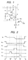
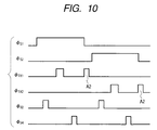
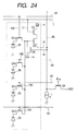
- the electric charge transfer switch Q1 is turned on and then turned off so that an electric charge generated by light in a photodiode 3 is transferred to the input portion of the amplifying transistor Q3, whereby the electric charge generated in the photodiode by light is added to the noise signal.
- the switch Q5 is a switch for giving a control pulse to turn on the reset switch Q2 and gives to the gate of the reset switch from a reference voltage source VDD, a voltage (ON-state voltage) not less than the threshold value sufficient to turn it on.
- Reference numeral 21 denotes a constant-current source as a load and comprises a mirror circuit, etc., but may be a load comprising a resistance, a transistor, etc.
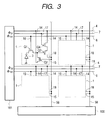
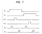
- the transfer switch Q1(n) of the unit cell of the n-th row is turned on and then off with the control pulse ⁇ TX2 so that the electric charge inside the photodiode is transferred to the input terminal of the source follower.
- the switch 24 is turned on so that an optical signal containing a noise signal is written into the holding capacity 25 for optical signals.
- the operation is as follows.
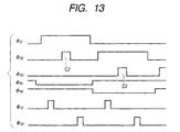
- the configuration and operation of the peripheral circuit 100 are the same as in Embodiment 2, and are as described above.
- the manufacturing yield regarding the conventional wiring was approximately 50%, but according to this embodiment it is estimated to rise approximately to 71%.
- the switch Q5 is turned off with a control pulse ⁇ VR.
- a control pulse ⁇ S1 a high level voltage is applied to the selecting switch line 67 of the (n-1)-th row to turn on the selecting switch Q4(n-1).
- the signal output line 58 is lowered to a low voltage by a constant-current load 21 of the source follower.
- the source follower operates and a voltage appearing in the signal output line 58 will become a voltage that has dropped from the reset voltage by a voltage equivalent to the threshold value voltage.
- the switch S2 is turned on and then off with a control pulse ⁇ 22, and the output voltage is written into a holding capacity 23 for noise signals as shown in FIG. 29 (period B1).
- the gate voltage of the reset switch Q2 will become lower by a voltage equivalent to the threshold value voltage than the source voltage of the reset switch Q2, so that the reset switch Q2 will be turned off.
- the switch Q5 is turned on with a control pulse ⁇ VR, and the voltage of the output signal line 58 is increased to such a voltage as to turn on the reset switch Q2.
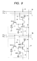
- FIG. 21 is a modification of Embodiment 1 wherein one output portion 2 comprising one source follower for signal amplification and a reset switch is disposed with regard to two photoelectric conversion portions and transfer switches.
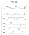
- FIG. 22 is a drive timing chart thereof.
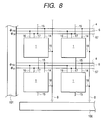
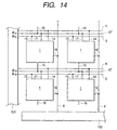
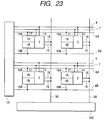
- FIG. 23 is a circuit diagram for a matrix of 2 rows by 2 columns of a solid image pickup device in which unit cells shown in FIG. 21 are arranged. In this embodiment, since a unit cell has two photoelectric conversion portions, one unit cell corresponds to two pixels. Therefore, in FIG. 22, there are four rows by four columns on the basis of number of pixels.
- each element configuring a unit cell comprises the same conductivity type element with electrons being used as transmission carriers.
- Reference numeral 88 denotes a P-type layer. With the conductivity type being made opposite in FIG. 33, elements using holes as transmission carriers can be used for configuration.
Landscapes
- Engineering & Computer Science (AREA)
- Multimedia (AREA)
- Signal Processing (AREA)
- Transforming Light Signals Into Electric Signals (AREA)
- Solid State Image Pick-Up Elements (AREA)
Priority Applications (1)
| Application Number | Priority Date | Filing Date | Title |
|---|---|---|---|
| EP10167170A EP2244295B1 (de) | 1999-10-05 | 2000-10-04 | Festkörperbildaufnahmevorrichtung |
Applications Claiming Priority (2)
| Application Number | Priority Date | Filing Date | Title |
|---|---|---|---|
| JP28446399 | 1999-10-05 | ||
| JP28446399 | 1999-10-05 |
Related Child Applications (1)
| Application Number | Title | Priority Date | Filing Date |
|---|---|---|---|
| EP10167170.9 Division-Into | 2010-06-24 |
Publications (3)
| Publication Number | Publication Date |
|---|---|
| EP1091409A2 true EP1091409A2 (de) | 2001-04-11 |
| EP1091409A3 EP1091409A3 (de) | 2006-10-18 |
| EP1091409B1 EP1091409B1 (de) | 2010-08-18 |
Family
ID=17678869
Family Applications (2)
| Application Number | Title | Priority Date | Filing Date |
|---|---|---|---|
| EP00308803A Expired - Lifetime EP1091409B1 (de) | 1999-10-05 | 2000-10-04 | Festkörperbildaufnahmevorrichtung und Bildaufnahmesystem |
| EP10167170A Expired - Lifetime EP2244295B1 (de) | 1999-10-05 | 2000-10-04 | Festkörperbildaufnahmevorrichtung |
Family Applications After (1)
| Application Number | Title | Priority Date | Filing Date |
|---|---|---|---|
| EP10167170A Expired - Lifetime EP2244295B1 (de) | 1999-10-05 | 2000-10-04 | Festkörperbildaufnahmevorrichtung |
Country Status (3)
| Country | Link |
|---|---|
| US (1) | US7081607B1 (de) |
| EP (2) | EP1091409B1 (de) |
| DE (1) | DE60044836D1 (de) |
Cited By (5)
| Publication number | Priority date | Publication date | Assignee | Title |
|---|---|---|---|---|
| GB2404440A (en) * | 2003-07-29 | 2005-02-02 | Agilent Technologies Inc | Circuit for an active pixel sensor |
| WO2006124384A1 (en) * | 2005-05-11 | 2006-11-23 | Micron Technology, Inc. | Split trunk pixel layout |
| EP2244295A1 (de) | 1999-10-05 | 2010-10-27 | Canon Kabushiki Kaisha | Festkörperbildaufnahmevorrichtung und Bildaufnahmesystem |
| CN105842813A (zh) * | 2015-01-30 | 2016-08-10 | 瑞萨电子株式会社 | 图像传感器 |
| EP3352220A4 (de) * | 2015-09-18 | 2019-08-07 | National University Corporation Shizuoka University | Halbleiterelement und festkörperbildaufnahmevorrichtung |
Families Citing this family (12)
| Publication number | Priority date | Publication date | Assignee | Title |
|---|---|---|---|---|
| US6965408B2 (en) | 2000-02-28 | 2005-11-15 | Canon Kabushiki Kaisha | Solid-state image pickup device having a photoelectric conversion unit and a punch-through current suppression circuit |
| JP3667214B2 (ja) * | 2000-08-25 | 2005-07-06 | キヤノン株式会社 | 固体撮像装置およびその駆動方法 |
| JP3792628B2 (ja) * | 2002-09-02 | 2006-07-05 | 富士通株式会社 | 固体撮像装置及び画像読み出し方法 |
| JP4194544B2 (ja) * | 2003-12-05 | 2008-12-10 | キヤノン株式会社 | 固体撮像装置及び固体撮像装置の駆動方法 |
| JP4144892B2 (ja) * | 2006-08-28 | 2008-09-03 | キヤノン株式会社 | 光電変換装置及び撮像装置 |
| JP5173503B2 (ja) * | 2008-03-14 | 2013-04-03 | キヤノン株式会社 | 撮像装置及び撮像システム |
| US8366318B2 (en) | 2009-07-17 | 2013-02-05 | Dental Imaging Technologies Corporation | Intraoral X-ray sensor with embedded standard computer interface |
| US9492129B2 (en) * | 2008-10-27 | 2016-11-15 | Dental Imaging Technologies Corporation | Triggering of intraoral X-ray sensor using pixel array sub-sampling |
| JP5458582B2 (ja) * | 2009-01-28 | 2014-04-02 | ソニー株式会社 | 固体撮像装置、固体撮像装置の駆動方法および電子機器 |
| US8829407B2 (en) * | 2010-10-19 | 2014-09-09 | Aptina Imaging Corporation | Imaging systems and methods including pixel arrays with reduced numbers of metal lines and control signals |
| US10225499B2 (en) * | 2016-04-11 | 2019-03-05 | Semiconductor Components Industries, Llc | Backside illuminated global shutter pixel with active reset |
| JP6909747B2 (ja) * | 2018-03-23 | 2021-07-28 | 株式会社東芝 | 固体撮像装置 |
Citations (3)
| Publication number | Priority date | Publication date | Assignee | Title |
|---|---|---|---|---|
| US5237423A (en) | 1990-11-29 | 1993-08-17 | Kabushiki Kaisha Toshiba | Multi-chip solid-state image sensing device |
| US5539461A (en) | 1993-03-23 | 1996-07-23 | Nippon Hoso Kyokai | Solid state image sensor and a driving method thereof |
| EP0908957A2 (de) | 1997-10-06 | 1999-04-14 | Canon Kabushiki Kaisha | Bildaufnahme-, Signaldetektion- und Signalakkumulierungsvorrichtung |
Family Cites Families (18)
| Publication number | Priority date | Publication date | Assignee | Title |
|---|---|---|---|---|
| JPS5678364U (de) * | 1979-11-14 | 1981-06-25 | ||
| EP0277016B1 (de) | 1987-01-29 | 1998-04-15 | Canon Kabushiki Kaisha | Photovoltaischer Wandler |
| US4959723A (en) | 1987-11-06 | 1990-09-25 | Canon Kabushiki Kaisha | Solid state image pickup apparatus having multi-phase scanning pulse to read out accumulated signal |
| US5406332A (en) | 1992-03-06 | 1995-04-11 | Canon Kabushiki Kaisha | Photoelectric converting device |
| EP0718889A3 (de) | 1992-06-25 | 1998-07-29 | Canon Kabushiki Kaisha | Photoelektrische Umwandlungsvorrichtung und Verfahren zu deren Herstellung |
| JPH0730084A (ja) | 1993-07-14 | 1995-01-31 | Fuji Xerox Co Ltd | 2次元密着型イメージセンサ |
| JP3758205B2 (ja) * | 1995-06-07 | 2006-03-22 | ソニー株式会社 | 固体撮像装置及びこれを用いたビデオカメラ、並びにx‐yアドレス型固体撮像装置の駆動方法 |
| EP0757475B1 (de) | 1995-08-02 | 2004-01-21 | Canon Kabushiki Kaisha | Halbleiter-Bildaufnehmer mit gemeinsamer Ausgangsleistung |
| JP3031606B2 (ja) * | 1995-08-02 | 2000-04-10 | キヤノン株式会社 | 固体撮像装置と画像撮像装置 |
| WO1997007630A1 (en) * | 1995-08-11 | 1997-02-27 | Kabushiki Kaisha Toshiba | Mos image pickup device |
| US5831258A (en) * | 1996-08-20 | 1998-11-03 | Xerox Corporation | Pixel circuit with integrated amplifer |
| US6002287A (en) | 1997-05-08 | 1999-12-14 | Canon Kabushiki Kaisha | Signal outputting apparatus |
| US5898168A (en) * | 1997-06-12 | 1999-04-27 | International Business Machines Corporation | Image sensor pixel circuit |
| JP4255527B2 (ja) | 1997-10-20 | 2009-04-15 | 株式会社半導体エネルギー研究所 | 半導体装置 |
| JP3571909B2 (ja) * | 1998-03-19 | 2004-09-29 | キヤノン株式会社 | 固体撮像装置及びその製造方法 |
| US6054704A (en) * | 1998-06-30 | 2000-04-25 | Foveon, Inc. | Driven capacitor storage pixel sensor and array |
| JP2000152086A (ja) | 1998-11-11 | 2000-05-30 | Canon Inc | 撮像装置および撮像システム |
| EP1091409B1 (de) | 1999-10-05 | 2010-08-18 | Canon Kabushiki Kaisha | Festkörperbildaufnahmevorrichtung und Bildaufnahmesystem |
-
2000
- 2000-10-04 EP EP00308803A patent/EP1091409B1/de not_active Expired - Lifetime
- 2000-10-04 DE DE60044836T patent/DE60044836D1/de not_active Expired - Lifetime
- 2000-10-04 US US09/678,025 patent/US7081607B1/en not_active Expired - Fee Related
- 2000-10-04 EP EP10167170A patent/EP2244295B1/de not_active Expired - Lifetime
Patent Citations (3)
| Publication number | Priority date | Publication date | Assignee | Title |
|---|---|---|---|---|
| US5237423A (en) | 1990-11-29 | 1993-08-17 | Kabushiki Kaisha Toshiba | Multi-chip solid-state image sensing device |
| US5539461A (en) | 1993-03-23 | 1996-07-23 | Nippon Hoso Kyokai | Solid state image sensor and a driving method thereof |
| EP0908957A2 (de) | 1997-10-06 | 1999-04-14 | Canon Kabushiki Kaisha | Bildaufnahme-, Signaldetektion- und Signalakkumulierungsvorrichtung |
Cited By (9)
| Publication number | Priority date | Publication date | Assignee | Title |
|---|---|---|---|---|
| EP2244295A1 (de) | 1999-10-05 | 2010-10-27 | Canon Kabushiki Kaisha | Festkörperbildaufnahmevorrichtung und Bildaufnahmesystem |
| GB2404440A (en) * | 2003-07-29 | 2005-02-02 | Agilent Technologies Inc | Circuit for an active pixel sensor |
| GB2404440B (en) * | 2003-07-29 | 2006-04-19 | Agilent Technologies Inc | Circuit for an active pixel sensor |
| WO2006124384A1 (en) * | 2005-05-11 | 2006-11-23 | Micron Technology, Inc. | Split trunk pixel layout |
| US7446357B2 (en) | 2005-05-11 | 2008-11-04 | Micron Technology, Inc. | Split trunk pixel layout |
| US8130301B2 (en) | 2005-05-11 | 2012-03-06 | Aptina Imaging Corporation | Split trunk pixel layout |
| CN105842813A (zh) * | 2015-01-30 | 2016-08-10 | 瑞萨电子株式会社 | 图像传感器 |
| EP3352220A4 (de) * | 2015-09-18 | 2019-08-07 | National University Corporation Shizuoka University | Halbleiterelement und festkörperbildaufnahmevorrichtung |
| US10453880B2 (en) | 2015-09-18 | 2019-10-22 | National University Corporation Shizuoka University | Semiconductor element and solid-state imaging device |
Also Published As
| Publication number | Publication date |
|---|---|
| EP1091409A3 (de) | 2006-10-18 |
| EP2244295A1 (de) | 2010-10-27 |
| EP1091409B1 (de) | 2010-08-18 |
| DE60044836D1 (de) | 2010-09-30 |
| US7081607B1 (en) | 2006-07-25 |
| EP2244295B1 (de) | 2011-12-21 |
Similar Documents
| Publication | Publication Date | Title |
|---|---|---|
| US7002626B2 (en) | Image sensor with motion artifact supression and anti-blooming | |
| EP1416721B1 (de) | Bildaufnahmevorrichtung | |
| US7091466B2 (en) | Apparatus and method for pixel binning in an image sensor | |
| US7081607B1 (en) | Solid state image pickup device and image pickup system | |
| JP4638097B2 (ja) | 画像センサ | |
| US8558931B2 (en) | Method and image sensor pixel without address transistor | |
| US7250970B2 (en) | Image pickup apparatus | |
| EP0977426B1 (de) | Aktiver Bildsensor mit von benachbarten Pixelzeilen gemeinsam genutzten Zeilensteuerbussen | |
| US7714920B2 (en) | Solid-state imaging device driving method | |
| US7148462B2 (en) | Pixel with differential readout | |
| KR100797506B1 (ko) | 증폭형 고체 촬상 장치 | |
| KR100678612B1 (ko) | 증폭형 고체 촬상 장치 | |
| US20120113305A1 (en) | Solid-state image pickup device and method of resetting the same | |
| US6697114B1 (en) | Triple slope pixel sensor and arry | |
| JP2000152086A (ja) | 撮像装置および撮像システム | |
| US20020024068A1 (en) | Solid-state image pickup apparatus | |
| JP3501743B2 (ja) | 固体撮像装置および撮像システム | |
| US7692702B2 (en) | Solid-state imaging device with amplifiers corresponding to signal lines and alternating control voltage | |
| US8319873B2 (en) | Solid-state imaging device | |
| US20050151867A1 (en) | Solid-state image pickup device with CMOS image sensor having amplified pixel arrangement | |
| JP2004104116A (ja) | 撮像装置 | |
| KR100444494B1 (ko) | 특성을 향상시킨 시모스 이미지센서의 단위화소 | |
| JP4618170B2 (ja) | 固体撮像装置 |
Legal Events
| Date | Code | Title | Description |
|---|---|---|---|
| PUAI | Public reference made under article 153(3) epc to a published international application that has entered the european phase |
Free format text: ORIGINAL CODE: 0009012 |
|
| AK | Designated contracting states |
Kind code of ref document: A2 Designated state(s): AT BE CH CY DE DK ES FI FR GB GR IE IT LI LU MC NL PT SE |
|
| AX | Request for extension of the european patent |
Free format text: AL;LT;LV;MK;RO;SI |
|
| PUAL | Search report despatched |
Free format text: ORIGINAL CODE: 0009013 |
|
| AK | Designated contracting states |
Kind code of ref document: A3 Designated state(s): AT BE CH CY DE DK ES FI FR GB GR IE IT LI LU MC NL PT SE |
|
| AX | Request for extension of the european patent |
Extension state: AL LT LV MK RO SI |
|
| 17P | Request for examination filed |
Effective date: 20070418 |
|
| AKX | Designation fees paid |
Designated state(s): DE FR GB IT NL |
|
| 17Q | First examination report despatched |
Effective date: 20070622 |
|
| GRAP | Despatch of communication of intention to grant a patent |
Free format text: ORIGINAL CODE: EPIDOSNIGR1 |
|
| GRAS | Grant fee paid |
Free format text: ORIGINAL CODE: EPIDOSNIGR3 |
|
| GRAA | (expected) grant |
Free format text: ORIGINAL CODE: 0009210 |
|
| AK | Designated contracting states |
Kind code of ref document: B1 Designated state(s): DE FR GB IT NL |
|
| REG | Reference to a national code |
Ref country code: GB Ref legal event code: FG4D |
|
| REF | Corresponds to: |
Ref document number: 60044836 Country of ref document: DE Date of ref document: 20100930 Kind code of ref document: P |
|
| REG | Reference to a national code |
Ref country code: NL Ref legal event code: VDEP Effective date: 20100818 |
|
| PG25 | Lapsed in a contracting state [announced via postgrant information from national office to epo] |
Ref country code: NL Free format text: LAPSE BECAUSE OF FAILURE TO SUBMIT A TRANSLATION OF THE DESCRIPTION OR TO PAY THE FEE WITHIN THE PRESCRIBED TIME-LIMIT Effective date: 20100818 |
|
| PG25 | Lapsed in a contracting state [announced via postgrant information from national office to epo] |
Ref country code: IT Free format text: LAPSE BECAUSE OF FAILURE TO SUBMIT A TRANSLATION OF THE DESCRIPTION OR TO PAY THE FEE WITHIN THE PRESCRIBED TIME-LIMIT Effective date: 20100818 |
|
| PLBE | No opposition filed within time limit |
Free format text: ORIGINAL CODE: 0009261 |
|
| STAA | Information on the status of an ep patent application or granted ep patent |
Free format text: STATUS: NO OPPOSITION FILED WITHIN TIME LIMIT |
|
| 26N | No opposition filed |
Effective date: 20110519 |
|
| PG25 | Lapsed in a contracting state [announced via postgrant information from national office to epo] |
Ref country code: FR Free format text: LAPSE BECAUSE OF NON-PAYMENT OF DUE FEES Effective date: 20101102 |
|
| REG | Reference to a national code |
Ref country code: FR Ref legal event code: ST Effective date: 20110630 |
|
| REG | Reference to a national code |
Ref country code: DE Ref legal event code: R097 Ref document number: 60044836 Country of ref document: DE Effective date: 20110519 |
|
| PGFP | Annual fee paid to national office [announced via postgrant information from national office to epo] |
Ref country code: GB Payment date: 20171101 Year of fee payment: 18 |
|
| PGFP | Annual fee paid to national office [announced via postgrant information from national office to epo] |
Ref country code: DE Payment date: 20171229 Year of fee payment: 18 |
|
| REG | Reference to a national code |
Ref country code: DE Ref legal event code: R119 Ref document number: 60044836 Country of ref document: DE |
|
| GBPC | Gb: european patent ceased through non-payment of renewal fee |
Effective date: 20181004 |
|
| PG25 | Lapsed in a contracting state [announced via postgrant information from national office to epo] |
Ref country code: DE Free format text: LAPSE BECAUSE OF NON-PAYMENT OF DUE FEES Effective date: 20190501 |
|
| PG25 | Lapsed in a contracting state [announced via postgrant information from national office to epo] |
Ref country code: GB Free format text: LAPSE BECAUSE OF NON-PAYMENT OF DUE FEES Effective date: 20181004 |