EP1091510A2 - Réseau de connexion pour des signaux à haute fréquence - Google Patents
Réseau de connexion pour des signaux à haute fréquence Download PDFInfo
- Publication number
- EP1091510A2 EP1091510A2 EP00121680A EP00121680A EP1091510A2 EP 1091510 A2 EP1091510 A2 EP 1091510A2 EP 00121680 A EP00121680 A EP 00121680A EP 00121680 A EP00121680 A EP 00121680A EP 1091510 A2 EP1091510 A2 EP 1091510A2
- Authority
- EP
- European Patent Office
- Prior art keywords
- coupling
- inputs
- outputs
- stage
- switching matrix
- Prior art date
- Legal status (The legal status is an assumption and is not a legal conclusion. Google has not performed a legal analysis and makes no representation as to the accuracy of the status listed.)
- Granted
Links
Images


Classifications
-
- H—ELECTRICITY
- H04—ELECTRIC COMMUNICATION TECHNIQUE
- H04B—TRANSMISSION
- H04B17/00—Monitoring; Testing
- H04B17/30—Monitoring; Testing of propagation channels
- H04B17/391—Modelling the propagation channel
-
- H—ELECTRICITY
- H04—ELECTRIC COMMUNICATION TECHNIQUE
- H04B—TRANSMISSION
- H04B17/00—Monitoring; Testing
- H04B17/20—Monitoring; Testing of receivers
- H04B17/23—Indication means, e.g. displays, alarms, audible means
Definitions
- the invention relates to a switching matrix for switching at least one High-frequency signal between at least one transceiver and at least one further transceiver according to the preamble of Claim 1.
- Such a switching matrix represents a radio field simulation, especially for the Mobile radio area and is used for field simulation for the test of Mobile radio equipment, such as transmitters and receivers from mobile radio base stations and mobile terminals.
- the invention has for its object a switching matrix of the aforementioned Art to improve in terms of functionality and manageability.
- the advantage of the invention is that a wide variety of test scenarios can be implemented without a great deal of wiring.
- the necessary coupling modules only have to be connected to one another in the desired manner by means of jumpers or plug connections. A high level of operating convenience is therefore achieved.
- the inputs and outputs of the coupling modules are advantageously routed to connecting sockets arranged on the front and / or rear wall of the housing.
- coupling modules are to be increased provided the switching matrix with another freely interconnectable four-pole hybrid coupler to be equipped with two inputs and two outputs, the Outputs of the second coupling stage via the hybrid coupler with the inputs of the third coupling stage can be connected as desired.
- the step attenuator Semiconductor components exist.
- Semiconductor attenuators also enable one uninterrupted switching, i.e. the signal is not during switching blanked out. This is particularly advantageous when performing series of measurements.
- Another advantage of semiconductor devices is the low level that can be achieved Total insertion loss of typically 17 to 25 dB depending on the connection of the Coupling modules. This means that signals from very weak signal sources can also be used are processed.
- Another preferred embodiment of the invention provides that the Damping values of the step attenuators directly via an attached to the housing Keypad are adjustable and / or can be changed in stages. This contributes to Increase in ease of use.
- the set damping can be displayed directly to the operator.
- the switching matrix is for a frequency range of approx. 800-2500 MHz designed. This large frequency range is made possible by the use of the most modern Semiconductor devices reached. This is the first time a test of dual band or Triband mobile terminals possible in the 900, 1800 and 2200 MHz range work.
- a further development of the invention provides that at the inputs or outputs the first coupling stage signal level display devices are arranged, which in simplest and preferred case an RF coupling element, an RF rectifier and a comparator or threshold circuit with at least one optical Include display element for the signal level. This allows the output to be used the optimal level, which is led to the subsequent coupling stages, simply determine.
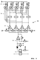
- FIG. 1 is the circuit diagram of a preferred embodiment of the switching matrix shown.
- the switching matrix according to the invention is designed as a passive system, so that bidirectional use is possible, i.e. each described below Signal input can also be a signal output and each described Signal output can be used as a signal input.
- the coupling stage A comprises, for example, four identical coupling modules A1 to A4, the coupling stage B. comprises two identical coupling modules B1, B2 and coupling stage C also two identical coupling modules C1, C2.
- each coupling module A1-A4 there can be a transceiver in it If a base station 1-4 (BTS) of the mobile network is connected.
- the Signal of the base stations 1-4 is in each case by a power divider 5-8 in four Signal branches divided, a signal branch directly to an output, e.g. Bu 1/4 each coupling module A1-A4 is guided.
- the other three signal branches are Signal attenuators 9a-9c, 10a-10c, 11a-11c, 12a-12c downstream, which the Attenuate the signal by 10 dB, 20 dB or 30 dB. Which weaken to different degrees Signals are sent to one output, e.g. Bu 1/1 to Bu 1/3 and so on.
- the coupling modules B1, B2 of the second coupling stage each comprise two inputs Bu 1/5, Bu 2/5 or Bu 3/5, Bu 4/5 and one downstream of each input Step attenuator 13, 14 or 15, 16, which is made up of semiconductor material.
- the Step attenuators have e.g. a control range of 0-63 dB in steps of 1 dB.
- the output signals of the stage attenuators 13, 14 and 15, 16 are over a power divider 17 and 18 merged and are each one Output 5/1 or 6/1 of modules B1, B2 available.
- the regulation of Damping per attenuator is done via a button on the front panel of the Device.
- the coupling modules C1 and C2 of the third coupling stage each include one Four-pole hybrid coupler 19 or 20 with 2 inputs 5/5, 5/3 or 6/5, 6/3 and two exits.
- the outputs of the hybrid couplers 19, 20 are each one Attenuators 21, 22 and 23, 24 on the outputs Bu 7/1, Bu 7/2 and Bu 7/3, Bu 7/4 of the coupling modules C1, C2 performed.
- the reducers have one Attenuation value of 10 dB.
- a further transceiver, e.g. in the form of a mobile terminal 28-31 connected become. There are two for free interconnection with the hybrid couplers 19, 20 Line terminations 26, 27 are provided in the form of 50 ohm loads.
- the switching matrix is free with another one interconnectable four-pole hybrid coupler 25 with two inputs Bu 5/2; Bu 6/2 and two Outputs Bu 5/4; Bu 6/4 equipped.
- FIG. 2 describes an application example of the switching matrix according to the invention, wherein the switching matrix according to Figure 1 for a test connection between one Mobile terminal 28 and four base stations 1-4 is wired. With this The handover behavior of the mobile terminal can be interconnected, for example 28 test.
- the base stations 1-4 are each connected to a coupling module A1-A4, the 10 dB outputs 1/3, 2/3, 3/3 and 4/3 of the coupling modules A1-A4 with the Inputs 1 / 5-4 / 5 of the coupling modules B 1 and B2 are connected.
- the outputs 5/1 and 6/1 of the coupling modules B1 and B2 are connected to the inputs 5/2 and 6/2 Hybrid 25 connected, an output 5/4 to the input 5/3 of the Coupling module C1 is performed.
- Coupling module C2 remains unused. On one Output 7/1 of the coupling module C1, the mobile radio terminal 28 is connected.
- a base station can also be used as a jammer misuse "to simulate interference interference.
- the switching matrix in the first coupling stage for the individual RF paths that described above from User-selectable pre-attenuation in 10 dB steps (0dB, 10dB, 20dB, 30dB), which are used for Adaptation of the entire path damping area is used.
- the user of the RF switching matrix must be aware of the transmission power level of the connected BTSs to control the range of the damping controller of the To be able to optimally use the RF switching matrix. That usually happens when There is a not exactly known RF attenuation between the device under test and the test site is a level measurement of the transmission power level of the connected BTSs Power meters or spectrum analyzers necessary.
- FIG. 3 shows, e.g. in the RF switching matrix to the entrance of everyone Damping paths via a coupler 33 (preferably a 3dB hybrid) that between the respective BTS connection 1-4 and the subsequent power splitter 5-8 is inserted a broadband RF rectifier 34 for power measurement connected.
- the output voltage of this HF rectifier 34 is determined by means of a comparator circuit 35 and a subsequent driver circuit 36 for Control of e.g. LEDs 37 evaluated such that a display by means of LEDs are made in the following way:
- LED 5 (e.g. color red) lights up when the one applied to the RF switching matrix Input power is too high (overload). This is the hint to the user insert an external (additional) attenuator for this path.
- Each of the built-in pre-attenuators e.g. 9a, 9b, 9c or each output Bu 1/1, Bu 1/2, etc.
- an LED in each attenuation path e.g. green
- the lighting of which lights up when the inputs BTSx of the HF Switching matrix with signals below the overdrive limit indicates which output of coupling module Ax is to be connected to the respective input Bu 1/5 - Bu 4/5 of coupling module Bx in order to achieve the optimum dynamic range of the switching matrix.
- LED1 is assigned to pre-attenuation 0dB
- LED2 to pre-attenuation 10dB
- LED4 to pre-attenuation 30dB.
- the switching matrix according to the invention can and is used in a variety of ways very easy to set up for a wide variety of test scenarios.
Landscapes
- Physics & Mathematics (AREA)
- Electromagnetism (AREA)
- Engineering & Computer Science (AREA)
- Computer Networks & Wireless Communication (AREA)
- Signal Processing (AREA)
- Monitoring And Testing Of Transmission In General (AREA)
- Input Circuits Of Receivers And Coupling Of Receivers And Audio Equipment (AREA)
- Control Of Motors That Do Not Use Commutators (AREA)
- Non-Reversible Transmitting Devices (AREA)
- Use Of Switch Circuits For Exchanges And Methods Of Control Of Multiplex Exchanges (AREA)
- Radio Relay Systems (AREA)
- Transceivers (AREA)
Applications Claiming Priority (2)
| Application Number | Priority Date | Filing Date | Title |
|---|---|---|---|
| DE19947654A DE19947654A1 (de) | 1999-10-04 | 1999-10-04 | Koppfelfeld für Hochfrequenzsignale |
| DE19947654 | 1999-10-04 |
Publications (3)
| Publication Number | Publication Date |
|---|---|
| EP1091510A2 true EP1091510A2 (fr) | 2001-04-11 |
| EP1091510A3 EP1091510A3 (fr) | 2003-09-03 |
| EP1091510B1 EP1091510B1 (fr) | 2005-05-25 |
Family
ID=7924367
Family Applications (1)
| Application Number | Title | Priority Date | Filing Date |
|---|---|---|---|
| EP00121680A Expired - Lifetime EP1091510B1 (fr) | 1999-10-04 | 2000-10-04 | Réseau de connexion pour des signaux à haute fréquence |
Country Status (4)
| Country | Link |
|---|---|
| US (1) | US6804200B1 (fr) |
| EP (1) | EP1091510B1 (fr) |
| AT (1) | ATE296508T1 (fr) |
| DE (2) | DE19947654A1 (fr) |
Cited By (1)
| Publication number | Priority date | Publication date | Assignee | Title |
|---|---|---|---|---|
| WO2005057972A1 (fr) * | 2003-12-12 | 2005-06-23 | Willtek Communications Gmbh | Procede et dispositif pour tester des telephones mobiles |
Families Citing this family (2)
| Publication number | Priority date | Publication date | Assignee | Title |
|---|---|---|---|---|
| KR101915526B1 (ko) * | 2012-04-17 | 2018-11-06 | 삼성전자 주식회사 | 휴대 단말기의 안테나 장치 |
| US8902902B2 (en) | 2012-07-18 | 2014-12-02 | Netronome Systems, Incorporated | Recursive lookup with a hardware trie structure that has no sequential logic elements |
Family Cites Families (6)
| Publication number | Priority date | Publication date | Assignee | Title |
|---|---|---|---|---|
| US5191594A (en) * | 1991-11-27 | 1993-03-02 | The United States Of America As Represented By The United States Department Of Energy | Fading channel simulator |
| US5465393A (en) * | 1993-04-12 | 1995-11-07 | Telefonaktiebolaget Lm Ericsson | Simulated air interface system for simulating radio communication |
| JPH08511097A (ja) * | 1993-06-07 | 1996-11-19 | マーチン コミュニケーションズ ピーティーワイ リミテッド | 多重路弱化試験信号を発生させるためのフェーディングシミュレータ及び方法 |
| KR100202502B1 (ko) * | 1996-12-30 | 1999-06-15 | 정장호 | 이동통신시스템 기지국의 시험회로 |
| KR100268231B1 (ko) * | 1998-05-30 | 2000-10-16 | 윤종용 | 무선 인터페이스 시뮬레이션 장치 및 방법 |
| JP3516663B2 (ja) * | 2001-02-26 | 2004-04-05 | 埼玉日本電気株式会社 | Cdma基地局試験装置及び基地局試験方法 |
-
1999
- 1999-10-04 DE DE19947654A patent/DE19947654A1/de not_active Withdrawn
-
2000
- 2000-10-04 EP EP00121680A patent/EP1091510B1/fr not_active Expired - Lifetime
- 2000-10-04 AT AT00121680T patent/ATE296508T1/de active
- 2000-10-04 DE DE50010382T patent/DE50010382D1/de not_active Expired - Lifetime
- 2000-10-04 US US09/679,655 patent/US6804200B1/en not_active Expired - Lifetime
Cited By (1)
| Publication number | Priority date | Publication date | Assignee | Title |
|---|---|---|---|---|
| WO2005057972A1 (fr) * | 2003-12-12 | 2005-06-23 | Willtek Communications Gmbh | Procede et dispositif pour tester des telephones mobiles |
Also Published As
| Publication number | Publication date |
|---|---|
| DE19947654A1 (de) | 2001-04-12 |
| US6804200B1 (en) | 2004-10-12 |
| EP1091510B1 (fr) | 2005-05-25 |
| EP1091510A3 (fr) | 2003-09-03 |
| ATE296508T1 (de) | 2005-06-15 |
| DE50010382D1 (de) | 2005-06-30 |
Similar Documents
| Publication | Publication Date | Title |
|---|---|---|
| DE69532373T2 (de) | Modulare Verbindungsmatrix für die matrische Verbindung von Antennen mit Funkkanaleinheiten | |
| DE19525430C2 (de) | Schaltungsnetzwerk-Meßeinrichtung und Verfahren zum Kalibrieren | |
| DE4327137C2 (de) | Stufendämpfungsglied | |
| DE102015115332A1 (de) | System und Verfahren für ein Richtkopplermodul | |
| EP0895300A2 (fr) | Coupleur d'antenne pour tester des téléphones mobiles | |
| DE69211330T2 (de) | Funksende- und -empfangsanordnung | |
| DE19528972B4 (de) | Serielle digitale Signalquelle mit einem Kabeldämpfungssimulator | |
| EP0810445B1 (fr) | Procédé pour la détermination de l'efficacité du blindage d'une portion de cable blindé | |
| EP1091510B1 (fr) | Réseau de connexion pour des signaux à haute fréquence | |
| WO2010066526A1 (fr) | Module frontal et procédé permettant de tester un module frontal | |
| EP2506563B1 (fr) | Dispositif de commutation | |
| DE102014223883B4 (de) | Mehrkanal-Drahtlosmikrofonsystem | |
| DE102016123474A1 (de) | RF-Modul und Verfahren zum Testen eines RF-Moduls | |
| EP0225461B1 (fr) | Réseau répartiteur de signaux pour habitations | |
| DE29917355U1 (de) | Koppelfeld für Hochfrequenzsignale | |
| DE69025293T2 (de) | Kombinier-/Sortiergerät für Radiofrequenzsignale | |
| DE4404046C2 (de) | Verfahren zum Kalibrieren eines zwei Meßtore aufweisenden Netzwerk-Analysators | |
| DE60218901T2 (de) | Verfahren und system zur übertragung von trägersignalen zwischen einem ersten und einem zweiten antennennetzwerk | |
| DE102005044620B4 (de) | Front-End-Modul für drahtlose Kommunikationsmittel | |
| DE112020005616T5 (de) | Frequenzkonverter-Zusatzteil für ein Test- und Messinstrument | |
| DE102023102665A1 (de) | Messsystem für hf-signale | |
| EP4016092B1 (fr) | Module de mesure de la puissance rf et porte-module comprenant le module de mesure de la puissance rf | |
| WO2016206980A1 (fr) | Dispositif et procédé de simulation de conditions d'erreurs dans une ligne | |
| DE10332808B4 (de) | Eichleitungs-Anordnung | |
| DE19706334A1 (de) | Logarithmische Umformschaltung |
Legal Events
| Date | Code | Title | Description |
|---|---|---|---|
| PUAI | Public reference made under article 153(3) epc to a published international application that has entered the european phase |
Free format text: ORIGINAL CODE: 0009012 |
|
| AK | Designated contracting states |
Kind code of ref document: A2 Designated state(s): AT BE CH CY DE DK ES FI FR GB GR IE IT LI LU MC NL PT SE |
|
| AX | Request for extension of the european patent |
Free format text: AL;LT;LV;MK;RO;SI |
|
| RAP1 | Party data changed (applicant data changed or rights of an application transferred) |
Owner name: T-MOBILE DEUTSCHLAND GMBH Owner name: MTS SYSTEMTECHNIK GMBH |
|
| PUAL | Search report despatched |
Free format text: ORIGINAL CODE: 0009013 |
|
| AK | Designated contracting states |
Kind code of ref document: A3 Designated state(s): AT BE CH CY DE DK ES FI FR GB GR IE IT LI LU MC NL PT SE |
|
| AX | Request for extension of the european patent |
Extension state: AL LT LV MK RO SI |
|
| 17P | Request for examination filed |
Effective date: 20031029 |
|
| 17Q | First examination report despatched |
Effective date: 20040406 |
|
| AKX | Designation fees paid |
Designated state(s): AT BE CH CY DE DK ES FI FR GB GR IE IT LI LU MC NL PT SE |
|
| GRAP | Despatch of communication of intention to grant a patent |
Free format text: ORIGINAL CODE: EPIDOSNIGR1 |
|
| GRAS | Grant fee paid |
Free format text: ORIGINAL CODE: EPIDOSNIGR3 |
|
| GRAA | (expected) grant |
Free format text: ORIGINAL CODE: 0009210 |
|
| AK | Designated contracting states |
Kind code of ref document: B1 Designated state(s): AT BE CH CY DE DK ES FI FR GB GR IE IT LI LU MC NL PT SE |
|
| PG25 | Lapsed in a contracting state [announced via postgrant information from national office to epo] |
Ref country code: IT Free format text: LAPSE BECAUSE OF FAILURE TO SUBMIT A TRANSLATION OF THE DESCRIPTION OR TO PAY THE FEE WITHIN THE PRESCRIBED TIME-LIMIT;WARNING: LAPSES OF ITALIAN PATENTS WITH EFFECTIVE DATE BEFORE 2007 MAY HAVE OCCURRED AT ANY TIME BEFORE 2007. THE CORRECT EFFECTIVE DATE MAY BE DIFFERENT FROM THE ONE RECORDED. Effective date: 20050525 Ref country code: IE Free format text: LAPSE BECAUSE OF FAILURE TO SUBMIT A TRANSLATION OF THE DESCRIPTION OR TO PAY THE FEE WITHIN THE PRESCRIBED TIME-LIMIT Effective date: 20050525 Ref country code: FI Free format text: LAPSE BECAUSE OF FAILURE TO SUBMIT A TRANSLATION OF THE DESCRIPTION OR TO PAY THE FEE WITHIN THE PRESCRIBED TIME-LIMIT Effective date: 20050525 |
|
| REG | Reference to a national code |
Ref country code: GB Ref legal event code: FG4D Free format text: NOT ENGLISH |
|
| REG | Reference to a national code |
Ref country code: CH Ref legal event code: EP |
|
| REG | Reference to a national code |
Ref country code: IE Ref legal event code: FG4D Free format text: LANGUAGE OF EP DOCUMENT: GERMAN |
|
| REF | Corresponds to: |
Ref document number: 50010382 Country of ref document: DE Date of ref document: 20050630 Kind code of ref document: P |
|
| PG25 | Lapsed in a contracting state [announced via postgrant information from national office to epo] |
Ref country code: DK Free format text: LAPSE BECAUSE OF FAILURE TO SUBMIT A TRANSLATION OF THE DESCRIPTION OR TO PAY THE FEE WITHIN THE PRESCRIBED TIME-LIMIT Effective date: 20050825 Ref country code: GR Free format text: LAPSE BECAUSE OF FAILURE TO SUBMIT A TRANSLATION OF THE DESCRIPTION OR TO PAY THE FEE WITHIN THE PRESCRIBED TIME-LIMIT Effective date: 20050825 Ref country code: SE Free format text: LAPSE BECAUSE OF FAILURE TO SUBMIT A TRANSLATION OF THE DESCRIPTION OR TO PAY THE FEE WITHIN THE PRESCRIBED TIME-LIMIT Effective date: 20050825 |
|
| PG25 | Lapsed in a contracting state [announced via postgrant information from national office to epo] |
Ref country code: ES Free format text: LAPSE BECAUSE OF FAILURE TO SUBMIT A TRANSLATION OF THE DESCRIPTION OR TO PAY THE FEE WITHIN THE PRESCRIBED TIME-LIMIT Effective date: 20050905 |
|
| PG25 | Lapsed in a contracting state [announced via postgrant information from national office to epo] |
Ref country code: CY Free format text: LAPSE BECAUSE OF FAILURE TO SUBMIT A TRANSLATION OF THE DESCRIPTION OR TO PAY THE FEE WITHIN THE PRESCRIBED TIME-LIMIT Effective date: 20051004 |
|
| GBT | Gb: translation of ep patent filed (gb section 77(6)(a)/1977) |
Effective date: 20050919 |
|
| PG25 | Lapsed in a contracting state [announced via postgrant information from national office to epo] |
Ref country code: PT Free format text: LAPSE BECAUSE OF FAILURE TO SUBMIT A TRANSLATION OF THE DESCRIPTION OR TO PAY THE FEE WITHIN THE PRESCRIBED TIME-LIMIT Effective date: 20051027 |
|
| PG25 | Lapsed in a contracting state [announced via postgrant information from national office to epo] |
Ref country code: LI Free format text: LAPSE BECAUSE OF NON-PAYMENT OF DUE FEES Effective date: 20051031 Ref country code: MC Free format text: LAPSE BECAUSE OF NON-PAYMENT OF DUE FEES Effective date: 20051031 Ref country code: LU Free format text: LAPSE BECAUSE OF NON-PAYMENT OF DUE FEES Effective date: 20051031 Ref country code: CH Free format text: LAPSE BECAUSE OF NON-PAYMENT OF DUE FEES Effective date: 20051031 Ref country code: BE Free format text: LAPSE BECAUSE OF NON-PAYMENT OF DUE FEES Effective date: 20051031 |
|
| REG | Reference to a national code |
Ref country code: IE Ref legal event code: FD4D |
|
| PLBE | No opposition filed within time limit |
Free format text: ORIGINAL CODE: 0009261 |
|
| STAA | Information on the status of an ep patent application or granted ep patent |
Free format text: STATUS: NO OPPOSITION FILED WITHIN TIME LIMIT |
|
| 26N | No opposition filed |
Effective date: 20060228 |
|
| REG | Reference to a national code |
Ref country code: CH Ref legal event code: PL |
|
| EN | Fr: translation not filed | ||
| BERE | Be: lapsed |
Owner name: MTS SYSTEMTECHNIK G.M.B.H. Effective date: 20051031 Owner name: T-MOBILE DEUTSCHLAND G.M.B.H. Effective date: 20051031 |
|
| PG25 | Lapsed in a contracting state [announced via postgrant information from national office to epo] |
Ref country code: FR Free format text: LAPSE BECAUSE OF NON-PAYMENT OF DUE FEES Effective date: 20051031 |
|
| PG25 | Lapsed in a contracting state [announced via postgrant information from national office to epo] |
Ref country code: FR Free format text: LAPSE BECAUSE OF NON-PAYMENT OF DUE FEES Effective date: 20050525 |
|
| PGFP | Annual fee paid to national office [announced via postgrant information from national office to epo] |
Ref country code: DE Payment date: 20191023 Year of fee payment: 20 Ref country code: NL Payment date: 20191022 Year of fee payment: 20 |
|
| PGFP | Annual fee paid to national office [announced via postgrant information from national office to epo] |
Ref country code: AT Payment date: 20191018 Year of fee payment: 20 |
|
| PGFP | Annual fee paid to national office [announced via postgrant information from national office to epo] |
Ref country code: GB Payment date: 20191023 Year of fee payment: 20 |
|
| REG | Reference to a national code |
Ref country code: DE Ref legal event code: R071 Ref document number: 50010382 Country of ref document: DE |
|
| REG | Reference to a national code |
Ref country code: NL Ref legal event code: MK Effective date: 20201003 |
|
| REG | Reference to a national code |
Ref country code: GB Ref legal event code: PE20 Expiry date: 20201003 |
|
| REG | Reference to a national code |
Ref country code: AT Ref legal event code: MK07 Ref document number: 296508 Country of ref document: AT Kind code of ref document: T Effective date: 20201004 |
|
| PG25 | Lapsed in a contracting state [announced via postgrant information from national office to epo] |
Ref country code: GB Free format text: LAPSE BECAUSE OF EXPIRATION OF PROTECTION Effective date: 20201003 |