EP1091571A2 - Vorrichtungen und Verfahren zur Erkennung und Kompensation von Beleuchtungsflimmern, Erkennung und Messung der Netzfrequenz - Google Patents
Vorrichtungen und Verfahren zur Erkennung und Kompensation von Beleuchtungsflimmern, Erkennung und Messung der Netzfrequenz Download PDFInfo
- Publication number
- EP1091571A2 EP1091571A2 EP00308844A EP00308844A EP1091571A2 EP 1091571 A2 EP1091571 A2 EP 1091571A2 EP 00308844 A EP00308844 A EP 00308844A EP 00308844 A EP00308844 A EP 00308844A EP 1091571 A2 EP1091571 A2 EP 1091571A2
- Authority
- EP
- European Patent Office
- Prior art keywords
- flicker
- frame
- video signal
- field
- result
- Prior art date
- Legal status (The legal status is an assumption and is not a legal conclusion. Google has not performed a legal analysis and makes no representation as to the accuracy of the status listed.)
- Granted
Links
Images









Classifications
-
- H—ELECTRICITY
- H04—ELECTRIC COMMUNICATION TECHNIQUE
- H04N—PICTORIAL COMMUNICATION, e.g. TELEVISION
- H04N23/00—Cameras or camera modules comprising electronic image sensors; Control thereof
- H04N23/70—Circuitry for compensating brightness variation in the scene
- H04N23/745—Detection of flicker frequency or suppression of flicker wherein the flicker is caused by illumination, e.g. due to fluorescent tube illumination or pulsed LED illumination
-
- H—ELECTRICITY
- H04—ELECTRIC COMMUNICATION TECHNIQUE
- H04N—PICTORIAL COMMUNICATION, e.g. TELEVISION
- H04N23/00—Cameras or camera modules comprising electronic image sensors; Control thereof
- H04N23/70—Circuitry for compensating brightness variation in the scene
Definitions
- This invention relates to an illumination flicker detection apparatus, an illumination flicker compensation apparatus, and an ac line frequency detection apparatus, methods of detecting illumination flicker, compensating flicker, and measuring ac line frequency.
- An illumination flicker detection apparatus for detecting flicker in a video signal which is generated by a video camera under illumination by fluorescent lamps are known. Moreover, a video signal processing apparatus for suppressing the affection by flicker in the video signal is also known.
- FIGs. 19A to 19D are illustrations of a prior art showing a relation between luminance changes of fluorescent lamps and the image shooting operation. If the cycle of the voltage of ac line is 50 Hz as shown in Fig. 19A, the luminance of a fluorescent lamp changes at 100 Hz as shown in Fig. 19B.
- Fig. 19C is an illustration showing operation of a prior art video camera. If a video camera or an electronic camera employing a MOS type of imager is used under illumination by fluorescent lamps at a shutter speed of 1/30 sec, charge storing timings and the luminance level of the video signal are shown in Fig. 19C.
- the MOS type of imager outputs a first line from timing A1 to B1 and a second line from timings A2 to B2 which timings A2 and B2 are slightly shifted in time base from the timings A1 and B1 as shown in Fig. 19C.
- the luminance level changes, so that a luminance level of the image changes at a cycle of 1/100 sec, which is sensed by a watcher as black stripes on the reproduced image.
- the reproduced image shows stripes over the to-be-reproduced image because the image storing timings are different with respect to the variation in the luminance of the fluorescent lamps every line.
- Figs. 20A to 20D are illustrations of a prior art showing a relation between luminance changes of fluorescent lamps and image shooting operation at 60 Hz. If the cycle of the voltage of ac line is 60 Hz as shown in Fig. 20A, the luminance of a fluorescent lamp changes at 120 Hz as shown in Fig. 20B.
- Fig. 20C is an illustration showing operation of a prior art video camera. If a video camera or an electronic camera employing a MOS type of imager is used under illumination by fluorescent lamps at a shutter speed of 1/50 sec, charge storing timings and the luminance level of the video signal are shown in Fig. 20C.
- rays entering respective pixels on a first line are converted into charges which are accumulated from timings A11 to B11 and charges on a second line are accumulated from timings A21 to B21 which timings A21 and B21 are slightly shifted in time base from the timingsA11 and B11.
- the luminance level changes, so that brightness level of the shot image changes, which is sensed by a watcher as black stripes on the reproduced image.
- a prior art flicker compensating apparatus for compensating the video signal is also known.
- Japanese patent application provisional publication No. 8-15324 discloses such a flicker compensating apparatus.
- This flicker compensating apparatus detects the presence or absence of flicker by an integrating result of a video signal at the present field and an integrating result of the video signal at the previous field and comparing the difference between the present and the previous fields with a threshold level and switching the shutter speed in accordance with the presence and the absence of flicker.
- the aim of the present invention is to provide superior illumination flicker detection apparatus, illumination flicker compensation apparatus and ac line frequency measuring apparatuses and superior methods of detecting illumination flicker, compensating flicker, and measuring ac line frequency.
- a first aspect of the present invention provides an illumination flicker detection apparatus comprising: integrating means for integrating levels of a video signal at pixels at each of unit areas included in a frame or field of said video signal; averaging means for averaging said integrated level at each of said unit areas at said frame or field and said integrated level at the corresponding unit area at an adjacent previous frame or field; dividing means for effecting division between results of said averaging and integrating means every unit area; and flicker judging means for judging whether flicker exists in said video signal by frequency-analyzing results of said dividing means at said unit areas and outputting a judging result.
- said unit area is a horizontal line.
- said unit area is a plurality of adjacent horizontal lines where variation in said levels due to said flicker is negligible.
- each of said unit areas includes a plurality of horizontal lines with interval at a frame, which horizontal line show the same phase in flicker component in said video signal.
- said averaging means comprising a circulation type of filter.
- said averaging means comprising a Finite Impulse Response filter.
- the illumination flicker detection apparatus further comprises: first summing means for summing said result of said integrating means at said frame or field and said result of said integrating means at another frame or field at every said unit area; and second summing means for summing said results of said averaging means at said frame or field and said result of said averaging means at said another frame or field at every unit area, wherein said another frame or field is prior to said frame or field by a predetermined number of frames or fields which is determined by a frequency of said flicker and a frame frequency of said video signal and said dividing means effects said division between said results of first and second summing means.
- the illumination flicker detection apparatus further comprises: first summing means for summing said results of said integrating means of a predetermined number of adjacent frames or fields at every unit area, said adjacent frames or fields including said frame or field; and second summing means for summing said results of said averaging means of said adjacent frames or fields at every unit area, wherein said dividing means effects said division between said results of first and second summing means.
- the illumination flicker detection apparatus further comprises another averaging means for averaging said results of said dividing means at a plurality of said unit areas at said frame or field, wherein each of said unit areas includes a plurality of horizontal lines with interval at a frame, said horizontal lines showing the same phase in flicker component in said video signal.
- the illumination flicker detection apparatus further comprises threshold level generating means for generating a threshold level in accordance with a shutter speed control signal which is used for generating said video signal, wherein said flicker judging means judges whether said flicker exists in said video signal using said threshold level.
- a second aspect of the present invention provides an illumination flicker compensation signal generation apparatus comprising: integrating means for integrating levels of a video signal at pixels at each of unit areas included in a frame or field of said video signal; averaging means for averaging said integrated level at each of said unit areas at said frame or field and said integrated level at the corresponding unit area at an adjacent frame or field; dividing means for effecting division between results of said averaging and integrating means every unit area; flicker judging means for judging whether flicker exists in said video signal by frequency-analyzing results of said dividing means at said unit areas and outputting a judging result; and flicker compensation means for generating a shutter speed control signal and an automatic gain controlling signal for generating said video signal in accordance with said judging result of said flicker judging means to compensate flicker in said video signal.
- a third aspect of the present invention provides a method of detecting flicker in a video signal comprising the steps of: (a) integrating video levels of a video signal at pixels at each of unit areas included in a frame or field of said video signal; (b) averaging said integrated level at each of said unit areas at said frame or field and said integrated level at the corresponding unit areas at an adjacent frame or field; (c) effecting division between results of said steps of (a) and (b) every unit area; and (d) judging whether flicker exists in said video signal by frequency-analyzing results of said step (c) at said unit areas and outputting a judging result.
- a fourth aspect of the present invention provides a method of compensating flicker in a video signal comprising the steps of: (a) integrating video levels of a video signal at pixels at each of unit areas included in a frame or field of said video signal; (b) averaging said integrated level at each of said unit areas at said frame or field and said integrated level at the corresponding unit areas at an adjacent frame or field; (c) effecting division between results of said steps of (a) and (b) every unit area; (d) judging whether flicker exists in said video signal by frequency-analyzing results of said step (c) at unit areas and outputting a judging result; and (e) generating a shutter speed control signal and an automatic gain controlling signal in accordance with said judging result of said step (d) to compensate flicker in said video signal.
- a fifth aspect of the present invention provides an illumination flicker detection apparatus comprising: integrating means for integrating levels of a video signal at pixels at each of unit areas included in a frame or field of said video signal; averaging means for averaging said integrated level at each of said unit areas at said frame or field and said integrated level at the corresponding unit area at an adjacent frame or field; still portion judging means for judging whether image at every block including a portion of said unit areas at a frame is still in accordance with result of said integrating means; dividing means for effecting division between results of said averaging and integrating means every unit area; and flicker judging means for judging whether flicker exists in said video signal in accordance with results of said dividing means and said still portion judging means.
- said unit area is a horizontal line.
- said unit area is a plurality of adjacent horizontal lines where variation of said video levels due to said flickering is negligible.
- said blocks are arranged in the vertical direction at a frame or a field, a vertical length of each block is determined in accordance with an integer times one cycle of illumination variation due to an ac line voltage, used for generating said video signal and a frame frequency of said video signal.
- still portion judging means may comprise: summing means for summing integration results of unit areas at every said block; variation detection means for detecting variation in result of said summing means between each of said blocks of the present frame or field and the corresponding block of a previous frame or field; and comparing means for comparing said variation with a threshold value, wherein said still portion judging means judges that image at each of said blocks is still when said variation is lower than said threshold value.
- said variation detection means may comprise: difference calculation means for calculating a difference in results of said summing means between each of said blocks of the present frame or field and the corresponding block of a previous frame or field; dividing means for dividing result of said difference calculating means by said result of said summing means of said present frame or field; and comparing means for comparing result of said dividing means with a threshold value, wherein said still portion judging means judges that image at each of said blocks is still when said result of said dividing means is lower than said threshold value.
- said variation detection means comprises: variation detection averaging means for averaging results of said summing means between present and previous frames or fields at each of said blocks; difference calculation means for calculating a difference in result of said summing means and said result of said variation detection averaging means; dividing means for dividing result of said difference calculating means by said result of said summing means of said present frame or field; and comparing means for comparing result of said dividing means with a threshold value, wherein said still portion judging means judges that image at every block areas is still when said result of said dividing means is lower than said threshold value.
- a sixth aspect of the present invention provides an illumination flicker compensation signal generation apparatus comprising: integrating means for integrating levels of a video signal at pixels at each of unit areas included in a frame or field of said video signal; averaging means for averaging said integrated level at each of said unit areas at said frame or field and said integrated level at the corresponding unit area of at least an adjacent frame or field; still portion judging means for judging whether image at every block including a portion of said unit areas at a frame is still in accordance with result of said integrating means; dividing means for effecting division between results of said averaging and integrating means every unit area; flicker judging means for judging whether flicker exists in said video signal in accordance with results of said dividing means and said still portion judging means; and flicker compensation means for generating a shutter speed control signal and an automatic gain controlling signal for generating said video signal in accordance with said judging result of said flicker judging means to compensate flicker in said video signal.
- a seventh aspect of the present invention provides a method of compensating flicker in a video signal comprising the steps of: (a) integrating levels of a video signal at pixels at each of unit areas included in a frame or field of said video signal; (b) averaging said integrated level at each of said unit areas at said frame or field and said integrated level at the corresponding unit area at an adjacent frame or field; (c) judging whether image at every block including a portion of said unit areas is still in accordance with result of said step (a); (d) effecting division between results of said steps of (a) and (b) every unit area; and (e) judging whether flicker exists in said video signal in accordance with results of said steps (c) and (d).
- an eighth aspect of the present invention provides a method of compensating flicker in a video signal comprising the steps of: (a) integrating levels of a video signal at pixels at each of unit areas included in a frame or field of said video signal; (b) averaging said integrated level at each of said unit areas at said frame or field and said integrated level at the corresponding unit area at an adjacent frame or field; (c) judging whether image at every block including a portion of said unit areas is still in accordance with result of said step (a); (d) effecting division between results of said steps of (a) and (b) every unit area; and (e) judging whether flicker exists in said video signal in accordance with results of said steps (c) and (d); and (f) generating a shutter speed control signal and an automatic gain controlling signal for generating said video signal in accordance with said judging result of said step (e) to compensate flicker in said video signal.
- a ninth aspect of the present invention provides an ac line frequency detection apparatus comprising: flicker component detection means for detecting a flicker component in a video signal generated with illumination of which luminance varies with ac line voltage; and flicker judging means for judging whether flicker exists in said video signal in accordance with said detected flicker component and outputting the judging result.
- said flicker component detection means comprises: integrating means for integrating levels of said video signal at pixels at each of unit areas included in a frame or field of said video signal; averaging means for averaging said integrated level at each of said unit areas at said frame or field and said integrated level at the corresponding unit area at an adjacent frame or field; dividing means for effecting division between results of said averaging and integrating means every unit area to output said detected flicker component.
- said flicker judging means comprises: variation analyzing means for analyzing variation of said detected flicker component with respect to horizontal lines.
- said flicker judging means comprises: spectrum analyzing means for analyzing spectrum of said flicker component.
- said unit area is a horizontal line.
- the ac line frequency measuring apparatus further comprises: imaging means for generating a video signal with illumination of which luminance varies with ac line voltage.
- a tenth aspect of the present invention provides a method of measuring an ac line frequency comprising the steps of: (a) detecting a flicker component in a video signal generated with illumination of which luminance varies with ac line voltage; and (b) judging whether flicker exists in said video signal in accordance with said detected flicker component.
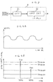
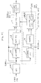
- Fig. 1 is a block diagram of an illumination flicker detection apparatus according to this invention.
- the illumination flicker detection apparatus includes an integrating circuit 1, an averaging unit 6 including a memory 2 and an averaging circuit 3, a dividing circuit 4, and a flicker judging circuit 5.
- a video signal is inputted to the integrating circuit 1.
- the integrating circuit 1 integrates pixel levels of a video signal in every horizontal line (unit area) at a frame (field).
- the memory 2 stores the integration result over a plurality of frames (fields).
- the averaging circuit 3 averages the integration results of horizontal lines at a plurality of frames (fields) from the integration result from the integrating circuit 1 and the memory 2.
- the dividing circuit 4 divides the integration results of horizontal lines by the averaged result of horizontal lines, respectively.
- the flicker judging circuit 5 judges whether illumination flicker exists in the video signal by frequency-analyzing the dividing results of horizontal lines.
- This illumination flicker detection apparatus is provided with a discrete circuit in this embodiment. However, the illumination flicker detection apparatus is also provided with a Digital Signal Processor (DSP), or a computer with a program.
- DSP Digital Signal Processor
- the video signal is generated by a video camera (not shown in Fig. 1) under illumination of which luminance varies in accordance with the voltage change of the ac line. That is, an image of an object illuminated by fluorescent lamps is shot by the video camera.
- Figs. 2A and 2B are illustration of the first embodiment.
- the integration circuit 1 integrates, accumulates, or averages the pixel levels (luminance level) at every horizontal line (unit area).
- the memory 2 successively stores a predetermined number of frames (fields) of the integration result.
- the averaging circuit 3 effects addition or averaging among SUM n,i from the integration circuit 1, SUM n-1,i , SUM n-2,i , and SUM n-3,i from the memory 2.
- Fig. 2B shows the summing or averaging operation from the integration results of the present frame and the previous frames.
- the memory 2 stores the integration result SUM n,i and outputs the integration results SUM n-1,i , SUM n-2,i , SUM n-3,i , at the i th line at frames n-1 to n-3.
- the averaging circuit 3 averages (sums) SUM ni , SUM n-1,i , SUM n-2,i , and SUM n-3,i . That is, the averaging circuit 3 averages the integrated level at each of the unit areas at the present frame or field and the integrated level at the corresponding unit area at an adjacent previous frame or field.
- the averaging result is represented as AVE n,i .
- the number of the previous frames per one unit averaging operation is three. However, it is also possible that, at least, the integration results of more than one previous frames are added to the integration result of the present frame.
- the dividing circuit 4 obtains SUM n,i / AVE n,i through calculation from the output SUM n,i of the integration circuit 1 and the output AVE n,i of the averaging circuit 3. That is, the dividing circuit 4 effects division between results of the averaging and integration every unit area.
- the flicker judging circuit 5 judges whether there is flicker with the dividing result of the dividing circuit 4.
- Fig. 3 is a block diagram of the flicker judging circuit 5.
- the flicker judging circuit 5 includes a DFT (Discrete Fourier Transform) circuit 21 supplied with the division result SUM n,i / AVE n,i and a comparing circuit 22 for comparing the output of the DFT circuit 21 with threshold values.
- DFT Discrete Fourier Transform
- Fig. 4A is a graphical drawing showing the output of the dividing circuit 4 according to the first embodiment, wherein the axis of abscissas represents line number at a frame and the axis of ordinates represents levels of dividing results, that is, SUM n,i /AVE n,i .
- the dividing results shows flicker.
- Fig. 4B is a graphical drawing showing the output of the DFT circuit 21 according to the first embodiment, wherein the axis of abscissas represents frequency and axis of ordinates represents levels of frequency components.
- the DFT circuit 21 effects Discrete Fourier Transform operation to output frequency components as shown in Fig. 4B from the division result of the division circuit 4.
- the line F 50 represents the level of the DFT circuit 21 at 50 Hz, i.e., component of 50 Hz
- the line F60 represents the level of the DFT circuit 21 at 60 Hz, i.e., component of 60 Hz.
- the comparing circuit 22 compares the results F 50 and F60 of the DFT circuit 21 with threshold levels TH 50-ON , TH 60-ON , TH 50-OFF , and TH 60-OFF . There are relations, TH 50-ON > TH 50-OFF and TH 60-ON > TH 60-OFF .
- the comparing circuit 22 compares the component F 50 with the threshold levels TH 50-ON and TH 50-OFF and the component F 60 with the threshold levels TH 60-ON and TH 60-OFF to detect flicker at 50Hz and 60 Hz in the video signal.
- the comparing circuit 22 judges the flicker as follows:
- the comparing circuit 22 judges there is flicker of 50 Hz.
- the comparing circuit 22 judges there is flicker of 60 Hz.
- the comparing circuit 22 judges that it is unknown that there is flicker.
- ⁇ is a weighting coefficient for flicker detection of 50 Hz and ⁇ is a weighting coefficient for flicker detection of 60 Hz. These coefficients are sufficiently greater than one, so that if the frequency component F 50 (F 60 ) is greater than the value of the weighting-coefficient-times the frequency component F 60 (F 50 ), the comparing circuit 22 judges there is flicker of 50 Hz (60 Hz). This reduces probability of erroneous judgment of existence of flicker due to luminance level change within a frame representing an image.
- the existence of flicker is judged from the average of integration values over a plurality of frames (fields) including the present frame at the corresponding lines.
- the flicker detection can be provided without influence of luminance level variation due to motion of the image.
- this structure (this method) provides illumination flicker detection of 60 Hz wherein luminance level variation.
- the integration circuit 1 integrates the pixel values every horizontal line.
- the integration circuit 1 integrates the pixel value on thinned horizontal lines, wherein thinning period is sufficiently shorter than the period of flicker (beat) component.
- the circuit stage after the integration circuit 1 effects the above-mentioned operation for the thinned horizontal lines.
- the capacity of the memory 2 can be reduced.
- An illumination flicker detection apparatus has substantially the same structure as that of the first embodiment.
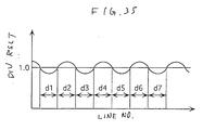
- the difference is that the integrating circuit 1b effects integration every a plurality of horizontal lines in which the flicker component level is considered to be substantially the same. That is, the video (luminance) levels of pixels are integrated or averaged every adjacent or consecutive three lines, i th , (i+1) th line, and (i+2) th line and outputted.
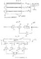
- Fig. 5 is an illustration of integration operation according to the second embodiment.
- FIGs. 6A and 6B show arrangements of color filters for single plate imagers and processing in this embodiment.
- the arrangement shown in Fig. 6A is for the complementary filter structure and the arrangement shown in Fig. 6B is a portion of Bayer arrangement for primary color filter structure.
- different color filters are arranged and adhered on imagers.
- a first line and a second line are alternately arranged, wherein a cyan filter Cy and a yellow filter ⁇ e are alternately arranged every pixel on the first line and a magenta filter Mg and a green filter are alternately arranged every pixel on the second line.
- a cyan filter Cy and a yellow filter ⁇ e are alternately arranged every pixel on the first line
- a magenta filter Mg and a green filter are alternately arranged every pixel on the second line.
- the video signal level in one block provides substantially the same level as the luminance signal.
- This signal similar to the luminance signal is integrated and the integrated result is used for detecting flicker, so that accurate flicker detection is provided.
- the video signal level in one block is substantially the same as the luminance signal ⁇ .
- This video signal similar to the luminance signal is integrated every a plurality of horizontal lines (two lines), so that accurate flicker detection is provided.
- the integration of video signal levels is effected every plural lines in which levels of flicker component can be considered as substantially the same.
- this structure reduces affection of luminance level variation of an object image, so that accurate flicker detection is provided.
- An illumination flicker detection apparatus has substantially the same structure as that of the first embodiment. The difference is that the integrating circuit 1c integrates the video levels of pixels on a plurality of horizontal lines which are apart from each other by a period in accordance with the flicker and frame frequencies.
- Fig. 7 is an illustration according to the third embodiment.
- the integrating circuit 1c integrates the video signal level on the horizontal lines (unit area) showing the same phase in the illumination flicker. That is, the integration circuit 1c integrates or averages video levels of pixels on the j th line, (j + p) th line, and (j + 2) th line. This level is represented as SUM nJ .
- the averaged value of the video levels of pixels on the j th line, (j + p) th line, and (j + 2) th line is represented as SUM nJ+1 .
- Each of the unit areas includes a plurality of horizontal lines with interval at a frame, which horizontal lines show the same phase in flicker component in said video signal.
- the number of the horizontal lines in each unit area is determined in accordance with the division of the flicker frequency (for example, 100Hz) by the frame frequency (for example, 30 HZ) when the flicker frequency is indivisible by the frame frequency.
- the video signal levels are integrated every a plurality of horizontal lines showing the same phase in the beat frequency between the illumination flicker and the frame cycle. Moreover, the integrated values are averaged over a plurality of frames including the present frame and previous frames and the averaged values are used in judging whether flicker is present. Thus, variation in luminance due to the image of an object can be reduced, so that accurate illumination flicker detection is provided. Moreover, the number of integration result SUM nJ is one third of the integration result SUM ni of the first embodiment. Thus, the capacity of the memory 2 can be reduced to one third.
- An illumination flicker detection apparatus has substantially the same structure as that of the first embodiment. The difference is that the averaging circuit 3b is used instead the averaging circuit 3 of the first embodiment.
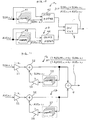
- Fig. 8 is a block diagram of the averaging unit 6b according to the fourth embodiment.
- the averaging unit 6b includes a multiplier 31, an adder 32, a memory 33, and a multiplier 34.
- the multiplier 31 multiplies the output SUM n,i of the integration circuit 1 by a coefficient (1 - k).
- the adder 32 adds an output of the multiplier 34 to the output of the multiplier 31.
- the memory 33 temporarily stores the output of the adder 32.
- the multiplier 34 multiplies an output AVE n,i of the memory 33 by the coefficient k.
- the coefficient k is a predetermined circular coefficient, wherein 0 ⁇ k ⁇ 1.
- the multiplier 31 multiplies the output SUM n,i of the integration circuit 1 by (1 - k) and supplies the result to the adder 32.
- the memory 33 stores one frame of the output of the adder 32 and outputs an averaged signal AVE n,i which is delayed by one frame from the output SUM n,i .
- the multiplier 34 multiplies the averaged signal AVE n,i by k.
- the adder 32 adds the output (1 - k) x SUM n,i to the output k x AVE n,i of the multiplier 34 and supplies the output to the memory 33.
- An illumination flicker detection apparatus has substantially the same structure as that of the first embodiment. The difference is that the averaging unit 6c is used instead the averaging unit 6 of the first embodiment.
- the averaging unit 6c includes an FIR (Finite Impulse Response) filter.
- Fig. 9 is a block diagram of the averaging unit 6c according to the fifth embodiment.
- the averaging unit 6c includes a memory 2c, multipliers 35 to 38, and an adder 39 as an FIR filter.
- the memory 2c outputs one-frame-delayed to three- frame-delayed integrated signals SUM n-1,i , SUM n-2,i , and SUM n-3,i .
- the multiplier 35 multiplies the integrated signal SUM n,i by ⁇ n .
- the multiplier 36 multiplies the one-frame-delayed integrated signal SUM n-1,i by ⁇ n-1 .
- the multiplier 37 multiplies the two-frame-delayed integrated signal SUM n-2,i by ⁇ n-2 .
- the multiplier 38 multiplies the three-frame-delayed integrated signal SUM n-3,i by ⁇ n -3 .
- This FIR type of averaging unit 6c provides illumination flicker detection by obtaining the averaged signal AVE n,i from integration result SUM n,i including such gradual change in luminance due to flicker at 60 Hz by setting the coefficients ⁇ n , ⁇ n-1 , ⁇ n-2 , ⁇ n-3 .
- averaging is effected with the FIR filter, so that the integrated data can be averaged with a desired characteristic.
- accurate illumination flicker detection is provided.
- An illumination flicker detection apparatus has substantially the same structure as that of the first embodiment. The difference is that the summing units 10a and 10b are further provided between the integration circuit 1 and the dividing circuit 4 and between the averaging circuit 3 and the dividing circuit 4, respectively.
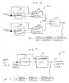
- Fig. 10 is a block diagram of the summing units 10a and 10b according to the sixth embodiment.
- the summing unit 10a includes a memory 41 storing the integrated signal SUM n,i and outputting a three-frame-delayed integrated signal SUM n-3,i and a first adder 42 for adding the three-frame delayed integrated signal SUM n-3,i to the integrated signal SUM n,i and supplies the adding result to the dividing circuit 4.
- the summing unit 10b includes a memory 43 storing the averaged signal AVE n,i and outputting a three-frame-delayed averaged signal and an adder 44 for adding the three-frame delayed averaged signal AVE n-3,i to the averaged signal AVE n,i and supplies the adding result to the dividing circuit 4.
- the dividing circuit 4 divides the adding result from the adder 42 by that from the adder 44.
- the integrated signal of the present frame is added to the integrated signal of the three-frame-delayed integrated signal and the averaged signal of the present frame is also added to the averaged signal of the three-frame-delayed averaged signal to remove the influence by the shot image of the object in the video signal.
- the integrated signal SUM n,i and the averaged signal AVE n,i are added to three-frame-delayed integrate signal SUM n-2,i and to the three-frame delayed averaged sigil AVE n-3,i , respectively.
- this is determined in accordance with the relation between the frequency of the ac line and the frame frequency of the video signal.
- this value is not limited to three.
- Fig. 11 is another example of summing units 11a and 11b according to the sixth embodiment.
- These summing units 11a and 11b employ circulation type filters.
- the summing unit 11a includes a multiplier 51, an adder 52, a memory 53, and a multiplier 54.
- the multiplier 51 multiplies the output SUM ni of the integration circuit 1 by a coefficient (1 - k 1 ).
- the adder 52 adds an output of the multiplier 54 to the output of the multiplier 51.
- the memory 53 stores the output of the adder 52 and supplies an output which is three-frame-delayed from the output of the adder 52.
- the multiplier 54 multiplies an output of the memory 53 by the coefficient k 1 .
- the coefficient k 1 is a predetermined circular coefficient, wherein 0 ⁇ k 1 ⁇ 1.
- the summing unit 11b includes a multiplier 55, an adder 56, a memory 57, and a multiplier 58.
- the multiplier 55 multiplies the output AVE n,i of the integration circuit 1 by a coefficient (1 - k 1 ).
- the adder 56 adds an output of the multiplier 58 to the output of the multiplier 55.
- the memory 57 stores the output of the adder 56 and supplies an output which is three-frame-delayed from the output of the adder 56.
- the multiplier 58 multiplies an output of the memory 57 by the coefficient k 1 .
- the coefficient k 1 is a predetermined circular coefficient, wherein 0 ⁇ k 1 ⁇ 1.
- the integrated signal of the present frame is added to the integrated signal of the three-frame-prior integrated signal and the averaged signal of the present frame is also added to the averaged signal of the three-frame-prior averaged signal to remove the affection due to the shot image of the object in the video signal.
- illumination flicker in the case of 50 Hz ac line and 1/30 sec frame period can be favorably detected.
- An illumination flicker detection apparatus has substantially the same structure as that of the first embodiment. The difference is that the summing units 12a and 12b are further provided.
- Fig. 12 is a block diagram of the summing units 12a and 12b according to the seventh embodiment.
- the summing unit 12a includes a memory 61 storing the integrated signal SUM n,i and outputting a one-frame-delayed integrated signal and a two-frame-delayed integrated signal and an adder 62 for effecting addition among the two-frame delayed integrated signal SUM n-2,i , the one-frame delayed integrated signal SUM n-1,i and the integrated signal SUM n,i and supplies the adding result to the dividing circuit 4.
- the summing unit 12b includes a memory 63 storing the averaged signal AVE n,i and outputs a one-frame-delayed averaged signal AVE n-1,i , a two-frame-delayed averaged signal AVE n-2,i , and an adder 64 for affection addition among the two-frame delayed averaged signal AVE n-2,i , the one-frame delayed averaged signal AVE n-1,i , and the averaged signal AVE n,i and supplies the adding result to the dividing circuit 4.
- the dividing circuit 4 divides the adding result from the adder 62 by that from the adder 64.
- the integrated signal of the present frame, the one-frame-delayed integrated signal, and the two-frame-delayed integrated signal are summed and the averaged signal of the present frame, the one-frame-delayed averaged signal, and the two-frame-delayed averaged signal are summed to provide stable dividing result.
- adjacent three frames of the integrated signal and the average signal are summed, respectively.
- the number of frames in summing is determined in accordance with the relation between the frequency of the ac line and the frame frequency of the video signal.
- the number of frames is not limited to three. Accordingly, illumination flicker developed in the condition that the frequency of the ac line is 60 Hz and the frame period is 1/30 sec can be favorably detected.
- An illumination flicker detection apparatus has substantially the same structure as that of the first embodiment. The difference is that the averaging block 13 is further provided.
- Fig. 13 is a block diagram of the averaging block according to the eighth embodiment.
- the averaging block includes a memory 72 and an averaging circuit 73.
- the memory 72 stores the dividing result from the dividing circuit 4 and when the inputted dividing result is j th line, the memory 72 outputs the delayed dividing results at the (j + p) th and (j + 2p) th horizontal lines on the same field.
- the averaging circuit 73 averages the dividing results of j th , (j + p) th , and (j + 2p) th horizontal lines.
- the averaging circuit 73 may be replaced with a median filter to filter the dividing results on the different horizontal lines at the same frame showing the same phase in the beat frequency of the flicker component.
- the averaged signal is supplied to the flicker judging circuit 5.
- the dividing results at the horizontal line showing the same phase of the flicker component at the same frame are averaged, so that affection in luminance variation level due to the shot image of the object in the video signal is removed.
- An illumination flicker detection apparatus has substantially the same structure as that of the first embodiment. The difference is that a threshold value processing circuit 82 is further provided to the flicker judging circuit 5b.
- the threshold value processing circuit 82 changes threshold values in accordance with a shutter speed signal which is also used for controlling the shutter speed of the imager generating the video signal supplied to the integration circuit 1.
- Fig. 14 is a block diagram of the flicker judging circuit 5b according to the ninth embodiment.
- the threshold value processing circuit 82 changes threshold values TH 50-ON , TH 60-ON , TH 50-OFF , and TH 60-OFF in accordance with the shutter speed signal to supply the changed values to the comparing circuit 22.
- Figs. 15A and 15C are graphical drawings showing the outputs of the dividing circuit 4 when the shutter speed is high and low, respectively.
- Figs. 15B and 15D are graphical drawings showing flicker components detected by the DFT circuit 81 when the shutter speed is high and low, respectively.
- the flicker components are relatively high when the shutter speed is high but the flicker components are relatively low when the shutter speed is low. Then, in this embodiment, the threshold values are set to be high when the shutter speed is high. On the other hand, when the shutter speed is low, the threshold values are set to be low in accordance with the shutter speed signal.
- the flicker components are judged more accurately by controlling the threshold values which are compared with the outputs of the DFT circuit 81.
- the shutter speed is changed, accurate illumination flicker judgment is provided.
- An illumination flicker compensation signal generation apparatus has substantially the same structure as that of the first to ninth embodiments. The difference is that a flicker compensation signal generation circuit 92 is further provided in addition to the illumination flicker detection apparatus according to the first to ninth embodiments.
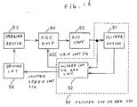
- Fig. 16 is a block diagram of an imaging apparatus according to the tenth embodiment.
- the flicker compensation signal generation apparatus 90 is structured as a portion of the imaging apparatus.
- the imaging apparatus includes an imaging device 93 such as MOS type imaging element, an AGC (automatic gain control) amplifier 94, an a/d converter 95, the flicker compensation signal generation apparatus 90, and a driving circuit 96.
- the flicker compensation signal generation apparatus 90 includes the flicker detection circuit 91 and the flicker compensation signal generation circuit 92.
- the imaging device 93 takes an image and generates the video signal. Particularly, the imaging device 93 takes an image of an object under illumination of which luminance varies with the periodical voltage variation of the ac line.
- the imaging device is driven by the driving circuit 96.
- the AGC amplifier 94 amplifies the video signal from the imaging device 93 with its gain controlled in accordance with an AGC gain control signal.
- the a/d converter 95 converts the video signal from the AGC amplifier 94 into a digital video signal.
- a flicker detection circuit 91 detects illumination flicker from the digital video signal as mentioned in the first to ninth embodiments.
- the flicker compensation signal generation circuit 92 performs illumination flicker compensation with the digital video signal from the a/d converter 95 and the detection result of the flicker detection circuit 91 by generating a shutter speed control signal supplied to the driving circuit 96 and the AGC gain control signal supplied to the AGC amplifier 94.
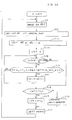
- Fig. 17 depicts a flow chart showing the operation of the flicker compensation signal generation circuit 92.
- step s1 when the flicker compensation signal generation circuit 92 detects power-on, the flicker compensation signal generation circuit 92 sets the mode of illumination flicker compensation to 50 Hz in step s2. Next, the flicker compensation signal generation circuit 92 repeatedly executes the operation in the loops including the steps s3 to s10.
- step s3 the flicker compensation signal generation circuit 92 obtains the video level of the digital video signal.
- step s4 the flicker compensation signal generation circuit 92 determines the AGC gain and the shutter speed and generates the AGC gain control signal and the shutter speed control signal.
- step s5 the flicker compensation signal generation circuit 92 obtains the illumination flicker detection result.
- step s6 the flicker compensation signal generation circuit 92 judges whether the illumination flicker frequency is 50 Hz. If the illumination flicker frequency is 50 Hz, the flicker compensation signal generation circuit 92 sets the mode of illumination flicker compensation to 50 Hz in step s8.
- the flicker compensation signal generation circuit 92 judges whether the illumination flicker frequency is 60 Hz in step s7. If the illumination flicker frequency is 60 Hz in step s7, the flicker compensation signal generation circuit 92 sets the mode of the illumination flicker to 60 Hz in step s9. If the illumination flicker frequency is not 60 Hz in step s7, the flicker compensation signal generation circuit 92 holds the mode as it is. After steps s8, s9, and s10, processing returns to step s3.
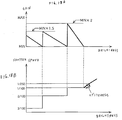
- Figs. 18A and 18B are graphical drawings showing the gain controlling and the shutter controlling referred in tenth and fifteenth embodiments.
- the flicker compensation signal generation circuit 92 controls the shutter speed and the AGC gain as shown in Figs. 18A and 18B in the 50 Hz mode.
- the flicker compensation signal generation circuit 92 obtains brightness in the video image of the digital video signal and determines the AGC gain and the shutter speed in accordance with the detected brightness and the flicker judgment result.
- "MIN" indicates the minimum value of the AGC gain
- the "MAX” indicates the maximum value of the AGC gain.
- the shutter speed is determined in accordance with the frame frequency (e.g., 30 Hz) and the frequency of the ac line voltage (e.g., 50 Hz).
- the shutter speed (interval) is 3/100 sec which is the lowest one of values which are integer times a half cycle of the ac line voltage.
- the flicker compensation signal generation circuit 92 instantaneously changes the shutter speed (interval) to 2/100 sec as shown in Fig. 18B.
- the flicker compensation signal generation circuit 92 changes the shutter speed to 3/2 times the minimum value, wherein "3/2" is an inverse number of the changing rate of the shutter speed. This prevents the rapidly changing in the brightness in the reproduced video image around shutter speed changing instance.
- the AGC gain is gradually reduced again.
- the flicker compensation signal generation circuit 92 instantaneously changes the shutter speed (interval) to 1/100 sec.
- the flicker compensation signal generation circuit 92 changes the shutter speed to twice the minimum value which is an inverse number of the changing rate of the shutter speed.
- the shutter speed reaches the maximum shutter speed without flicker, that is, 1/100 sec in 50 Hz, and the AGC gain is minimum, the shutter speed is increased (shutter interval is reduced) from 1/100 sec. On the other hand, the AGC gain is held. Thus, the brightness in the video signal is not saturated, so that the dynamic range can be increased.
- hysteresis is provided between the shutter speed of 1/100 sec and higher shutter speeds (e.g., 1/250 sec).
- the shutter speed is set to values which are integer times the half cycle of the ac line voltage, that is, 1/120 sec, 2/120 sec, 3/120 sec ⁇ .
- the AGC amplifier 94 is provided and the gain controlling is effected in the analog manner.
- a digital AGC control circuit is provided after the a/d converter 95 instead the AGC amplifier 94 and the digital AGC control circuit is controlled in accordance with the AGC gain control signal (data).
- the averaging unit 6 effects averaging with the integrated values of the present frame and the previous frames.
- illumination flicker is detected with MOS type of imager.
- this invention is applicable to the video signal generated from CCD imaging devices.
- the illumination flicker detection apparatus and the method of detecting flicker it is possible to detect illumination flicker developed during shooting images under illumination by ac line voltage without affection due to luminance level change of an object in the images because the video signal levels in a plurality of frames are averaged and the flicker existent judgment is effected in accordance with the averaged value. Moreover, the illumination flicker detection in the case of 60 Hz of ac lines at the frame frequency of 30 Hz can be provided.
- the shutter speed and the AGC gain are controlled in accordance with the video signal level of the inputted video signal and the detected flicker frequency to compensate brightness change due to illumination flicker. Moreover, only the shutter speed is further controlled when the brightness is sufficiently high. This prevents a trouble in the reproduced image when the brightness is high.
- Fig. 21 is a block diagram of an illumination flicker detection apparatus according to the eleventh embodiment.
- the illumination flicker detection apparatus includes the integrating circuit 1, the averaging unit 6 including the memory 2b and the averaging circuit 3, the dividing circuit 11, the flicker judging circuit 5, and a still portion judging unit 15.
- a video signal is inputted to the integrating circuit 1.
- the integrating circuit 1 integrates pixel levels in every horizontal line (unit area) in a frame from the video signal.
- the memory 2b stores the integration result over a plurality of frames (fields).
- the averaging circuit 3 averages the integration results of horizontal lines at a plurality of frames (fields) from the integration result from the integrating circuit 1 and the memory 2b.
- the dividing circuit 11 divides the integration results of horizontal lines by the averaged result of horizontal lines, respectively, when the still portion judging unit 15 detects a still portion.
- the flicker judging circuit 5 judges whether flicker exists in the video signal by frequency-analyzing the dividing results of horizontal lines.
- This illumination flicker detection apparatus is provided with a discrete circuit in this embodiment. However, the illumination flicker detection apparatus is also provided with a Digital Signal Processor (DSP), or a computer with a program.
- DSP Digital Signal Processor
- the video signal is generated by a video camera (not shown in Fig. 21) under illumination of which luminance varies in accordance with the voltage change of the ac line. That is, an image of an object illuminated by fluorescent lamps is shot by the video camera.
- the integration circuit 1 integrates, accumulates, or averages the pixel levels (luminance level) at every horizontal line.
- the memory 2b successively stores a predetermined number of frames (fields) of the integration result.
- the averaging circuit 3 effects addition or averaging among SUM n-1,i , SUM n-2,i , and SUM n-3,i from the memory 2b.
- Fig. 22 shows the summing or averaging operation from the integration results of the previous frames.
- the memory 2b stores the integration result SUM n,i and outputs the integration results SUM n-1,i , SUM n-2,i , SUM n-3,i at the i th line at frames n-1 to n-3.
- the averaging result is represented as AV n,i .
- the number of the previous frames per one unit averaging operation is three.
- the dividing circuit 11 obtains SUM n,i /AV n,i through calculation from the output SUM n,i of the integration circuit 1 and the output AV n,i of the averaging circuit 3d when the still portion judging unit judges that the block is still.
- the flicker judging circuit 5 judges whether there is flickering with the dividing result of the dividing circuit 11.
- Fig. 23 is a block diagram of the flicker judging circuit 5 according to the eleventh embodiment.
- the flicker judging circuit 5 includes the DFT (Discrete Fourier Transform) circuit 21, supplied with the integration result SUM n,i and the averaging result AV n,i, for detecting frequency component levels and the comparing circuit 22 for comparing the output of the DFT circuit 21 with threshold values.
- DFT Discrete Fourier Transform
- the still portion judging unit 15 includes a summing circuit 7, a memory 8, and a still portion judging circuit 9.
- the still portions judging unit 15 detects a still portion at the image on the screen using the output of the integrations circuit 1.
- the summing circuit 7 sums the integration results of lines included in N cycles of the flicker component at a frame.
- the summing results of the summing circuit 7 obtained as mentioned above are the same with respect to periodical variation in the luminance of the light source.
- Fig. 25 is an illustration showing the operation of the still portion judging circuit 9.
- the memory 8 temporally stores the summing results of several frames.
- the still portion judging circuit 9 calculates difference between the summing result B-SUM nj of the present frame from the summing circuit 7 and the one-frame-prior summing result B-SUM n-1,j from the memory 8 and compares the difference with a threshold value TH 1 . When the difference is lower than the threshold value TH 1 , the still portion judging circuit 9 judges the block is still portion.
- the difference represents variation or movement of the image of an object at the still portion judging block. Therefore, the still portion judging block is judged to be still when the difference is lower than the threshold value TH 1 .
- the dividing circuit 11 calculates division SUM ni /AV ni from the output SUM ni of the integration circuit 1 and the output AV ni of the averaging circuit 3d when the difference is lower than the threshold value TH 1 .
- the dividing circuit 11 does not output the dividing result.
- Fig. 4A shows the output of the dividing circuit 11 according to the eleventh embodiment, wherein the axis of abscissas represents line number at a frame and the axis of ordinates represents levels of dividing results, that is, SUM n,i /AV n,i .
- the dividing results shows flickering.
- Fig. 4B shows the output of the DFT circuit 21 according to the first embodiment, wherein the axis of abscissas represents frequency and axis of ordinates represents levels of frequency components.
- the line F 50 represents the level of the DFT circuit 21 at 50 Hz, i.e., component of 50 Hz and the line F60 represents the level of the DFT circuit 21 at 60 Hz, i.e., component of 60 Hz.
- the comparing circuit 22 compares the results F 50 and F 60 of the DFT circuit 21 with threshold levels TH 50-ON , TH 60-ON , TH 50-OFF , and TH 60-OFF . There are relations, TH 50-ON > TH 50-OFF and TH 60-ON > TH 60-OFF .
- the comparing circuit 22 compares the component F 50 with the threshold levels TH 50-ON and TH 50-OFF and the component F 60 with the threshold levels TH 60-ON and TH 60-OFF to detect flicker in the video signal.
- the comparing circuit 22 judges the flicker as follows:
- the comparing circuit 22 judges there is flicker of 50 Hz.
- the comparing circuit 22 judges there is flicker of 60 Hz.
- the comparing circuit 22 judges that it is unknown that there is flicker.
- ⁇ is a weighting coefficient for flicker detection of 50 Hz and ⁇ is a weighting coefficient for flicker detection of 60 Hz. These coefficients are sufficiently greater than one, so that if the frequency component F 50 (F 60 ) is greater than the value of the weighting-coefficient-times the frequency component F 60 (F 50 ), the comparing circuit 22 judges there is flicker of 50 Hz (60 Hz). This reduces probability of erroneous judgment of existence of flicker due to luminance level change within a frame representing an image.
- the existence of flicker is judged from the average of integration values over a plurality of frames (fields) including the present frame at the corresponding lines.
- the flicker detection can be provided without affection of luminance level variation due to motion of the image.
- this structure (this method) provides illumination flicker detection of 60 Hz wherein luminance level variation.
- the integration circuit 1 integrates the pixel values every horizontal line.
- the integration circuit 1 integrates the pixel value on thinned horizontal lines, wherein thinning period is sufficiently shorter than the period of flicker (beat) component.
- the circuit stage after the integration circuit 1 effects the above-mentioned operation for the thinned horizontal lines.
- the capacity of the memory 2b can be reduced.
- the still portion judging unit 15 supplies the result of still portions to the dividing circuit 11.
- An illumination flicker detection apparatus has substantially the same structure as that of the eleventh embodiment.
- the difference is that the integrating circuit 1d effects integration every a plurality of horizontal lines in which the flicker component level is considered to be substantially the same. That is, the video (luminance) levels of pixels are integrated every adjacent or consecutive lines.
- Fig. 26 is an illustration showing the operation of the integration circuit 1d according to the twelfth embodiment.
- the integration circuit 1d integrates or averages the video (luminance) level of pixels every block (in the drawing, left portions of the two consecutive horizontal lines) in which the flicker component level is considered to be substantially the same.
- the area at which the flicker component level is considered to be substantially the same is referred to as a block.
- the integrated or averaged value of the video level of all effective pixels at the i th block at nth frame is represented by SUM n,bi .
- Fig. 27 is an illustration showing the summing or averaging operation from the integration results of the present frame and the previous frames.
- the memory 2b stores the integration result SUM n,bi and outputs the integration results SUM n-1,bi , SUM n-2,bi , SUM n-3,bi at the i th block at frames n-1 to n-3.
- the averaging circuit 3d shown in Fig. 21, averages (sums) SUM n-1,i , SUM n-2,i , and SUM n-3,i .
- the averaging result is represented as AV n,i .
- the number of the previous frames per one unit averaging operation is three. However, it is also possible that, at least, the integration results of more than one previous frames are summed.
- Fig. 28 is an illustration showing the summing operation according to the twelfth embodiment.
- the summing circuit 7 sums the integration results of horizontal lines at the still portion judging block corresponding to N cycles of the flicker component at a frame.
- the summing circuit 7 sums the integration results of q blocks at j th still portion judging block. It is assumed that the number of the top block is m.
- N is a natural number from 1 to 3 when the ac line frequency is 50 Hz and the frame frequency is 30 Hz.
- the summing result of the blocks (horizontal lines) corresponding to N cycle of the flicker component shows the same luminance level with respect to the flickering.
- Fig. 29 is an illustration showing the still portion judging operations according to the twelfth embodiment.
- the still portion judging circuit 9 calculates difference between the summing result B-SUMnbj and the one-frame-prior summing result B-SUM n-1 read from the memory 8 and compares the difference with the threshold value TH 1 . When the difference is lower than the threshold value TH 1 the still portion judging circuit 9 judges the still portion judging block is in the still condition.
- the still portion judging circuit 9 supplies the judging result to the dividing circuit 11.
- the dividing circuit 11 calculates SUM nbi /AV nbi only when the still portion judging block is judged to be still.
- the flicker judging circuit 5 judges the existence of flicker in accordance with the result SUM nbi /AV nbi of the dividing circuit 11 as mentioned above.
- FIGs. 6A and 6B show arrangements of color filters for single plate imagers and processing in this embodiment.
- the arrangement shown in Fig. 6A is for the complementary filter structure and the arrangement shown in Fig. 6B is a portion of Bayer arrangement for primary color filter structure.
- different color filters are arranged and adhered on imagers.
- a first line and a second line are alternately arranged, wherein a cyan filter Cy and a yellow filter Ye are alternately arranged every pixel on the first line and a magenta filter Mg and a green filter are alternately arranged every pixel on the second line.
- a cyan filter Cy and a yellow filter Ye are alternately arranged every pixel on the first line
- a magenta filter Mg and a green filter are alternately arranged every pixel on the second line.
- the video signal level in one block provides substantially the same level as the luminance signal.
- This signal similar to the luminance signal is integrated and the integrated result is used for detecting flicker, so that accurate flicker detection is provided.
- the video signal level in one block is substantially the same as the luminance signal ⁇ .
- This video signal similar to the luminance signal is integrated every a plurality of horizontal lines (two lines), so that accurate flicker detection is provided.
- the integration of video signal levels is effected every area in which flicker components can be considered as substantially the same. Further, the integration results are summed every still portion judging block and the difference between the summing results of the present frame and the previous frame is calculated. Only when the difference is lower than the threshold TH 1 , the dividing circuit effect dividing. The flicker judging circuit 5 judges the existence of flier in accordance with the dividing result.
- the still portion judging circuit 9 controls the dividing circuit 11.
- the still portion judging circuit 9 may control the flicker judging circuit 5. That is, division is effected irrespective of the still portion judging result.
- the flicker judging circuit 5 judges (outputs) the existence of flier only when the still portion judging block is judged to be still.
- the outputting result of the flicker judging circuit 5 may be controlled in accordance with the output of the still portion judging circuit 9.
- An illumination flicker detection apparatus has substantially the same structure as that of the eleventh embodiment. The difference is that a dividing circuit 32 is further provided in the still portion judging unit 15.
- Fig. 30 is a block diagram of the still portion judging circuit 9b.
- the still portion judging circuit 9b includes a difference calculating circuit 31, a dividing circuit 32, and a comparing circuit 32.
- the difference calculating circuit 31 calculates a difference between the summing result B-SUM nj of the present frame and the summing result of the one-frame-previous frame B-SUM n-1j .
- the dividing circuit 32 divides the difference from the difference calculation circuit 31 by the summing result from the summing circuit 7.
- the dividing result is supplied to the comparing circuit 33.
- the dividing result is given by:
- the comparing circuit 33 compares the dividing result with a threshold value TH 2 .
- the J th still portion judging block is judged to be still by the comparing circuit 33.
- the judging result of the still portion judging unit 15, i.e., the output of the comparing circuit 33 is supplied to the dividing circuit 11.
- the dividing circuit 11 and the flicker judging circuit 5 judges flicker as similarly as the eleventh embodiment.
- the ratio between the summing result of the present frame and the one-frame-previous summing result and the ration, that is, the dividing result is compared with the threshold TH 2 .
- An illumination flicker detection apparatus has substantially the same structure as that of the thirteenth embodiment. The difference is that an averaging circuit 41 and a difference calculation circuit 42 are further provided in the still portion judging circuit 9c.
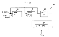
- Fig. 31 is a block diagram of the still portion judging unit 15 according to the fourteenth embodiment.
- the still portion judging unit 15 includes the averaging circuit 41 for averaging the summing result of the summing circuit 7 and the one-frame-previous summing result and two-frame-previous summing result from the memory 8, the difference calculating circuit 42 for calculating a difference between the summing result of the present frame and the averaging result B-AVE nj of the averaging circuit 41, a dividing circuit 43 for dividing the difference by the summing result of the present frame, and a comparing circuit 44 compares the dividing result from the dividing circuit 43 with a threshold TH3.
- the difference calculating circuit 42 calculates a difference between the summing result B-SUM nj of the present frame and the averaging result AVE nj of the averaging circuit 41.
- the dividing circuit 43 divides the difference by the summing result B-SUM nj of the present frame. The dividing result is given by:
- the comparing circuit 44 compares the dividing result from the dividing circuit 43 with a threshold TH3. When the dividing result is lower than the threshold TH3, the still portion judging unit 15 judges the still portion judging block is still.
- the judging result of the still portion judging unit 15, i.e., the output of the comparing circuit 44 is supplied to the dividing circuit 11.
- the dividing circuit 11 and the flicker judging circuit 5 judges flicker as similarly as the eleventh embodiment.
- a ratio between the summing result B-SUM nj of the present frame and the averaging result B-AVE nj derived by averaging the previous frames of summing results and the ratio is compared with the threshold TH3; so that video level of the previous frames to be compared with that of the present frame becomes stable.
- the still portion can be more accurately judged.
- accuracy of flicker detection at 50 Hz and 60 Hz is improved.
- the difference is divided by the summing result B-SUM nj of the present frame.
- dividing the averaging result B-AVEnj instead the summing result B-SUMnj of the present frame provides the similar effect.
- the averaging circuit 41 may be provided with the circulation type of filter or the FIR filter.
- An illumination flicker compensation signal generation apparatus has substantially the same structure as that of the eleventh to fourteenth embodiments. The difference is that a flicker compensation signal generation circuit 192 is provided in addition to the illumination flicker detection apparatus 190 according to the eleventh to fourteenth embodiments.
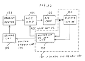
- Fig. 32 is a block diagram of an imaging apparatus according to the fifteenth embodiment.
- the flicker compensation signal generation apparatus 190 is structured as a portion of the imaging apparatus.
- the imaging apparatus includes an imaging device 193 such as MOS type imaging element, an AGC (automatic gain control) amplifier 194, an a/d converter 195, the flicker compensation signal generation apparatus 190, and a driving circuit 196.
- the flicker compensation signal generation apparatus 190 includes the flicker detection circuit 191 and the flicker compensation signal generation circuit 192.
- the imaging device 193 takes an image and generates the video signal. Occasionally, the imaging device 193 takes an image of an object under illumination of which luminance varies with the periodical voltage variation of the ac line.
- the imaging device 193 is driven by the driving circuit 196.
- the AGC amplifier 194 amplifies the video signal from the imaging device 193 with its gain controlled in accordance with an AGC gain control signal.
- the a/d converter 195 converts the video signal from the AGC amplifier 194 into a digital video signal.
- a flicker detection circuit 191 detects illumination flicker from the digital video signal as mentioned in the eleventh to fourteenth embodiments.
- the flicker compensation signal generation circuit 192 performs illumination flicker compensation with the digital video signal from the a/d converter 195 and the detection result of the flicker detection circuit 191 by generating a shutter speed control signal supplied to the driving circuit 196 and the AGC gain control signal supplied to the AGC amplifier 194.
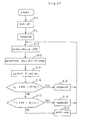
- Fig. 33 depicts a flow chart showing the operation of the flicker compensation signal generation circuit 192 according to the fifteenth embodiment.
- step s11 when the flicker compensation signal generation circuit 192 detects power-on, the flicker compensation signal generation circuit 192 sets the mode of illumination flicker compensation to 50 Hz in step s12. Next, the flicker compensation signal generation circuit 192 repeatedly executes the operation in the loops including the steps s13 to s20.
- the flicker compensation signal generation circuit 192 obtains the video level of the digital video signal.
- the flicker compensation signal generation circuit 192 determines the AGC gain and the shutter speed and generates the AGC gain control signal and the shutter speed control signal.
- the flicker compensation signal generation circuit 192 obtains the illumination flicker detection result.
- the flicker compensation signal generation circuit 192 judges whether the illumination flicker frequency is 50 Hz. If the illumination flicker frequency is 50 Hz, the flicker compensation signal generation circuit 192 sets the mode of illumination flicker compensation to 50 Hz in step s18.
- the flicker compensation signal generation circuit 192 judges whether the illumination flicker frequency is 60 Hz in step s17. If the illumination flicker frequency is 60 Hz in step s17, the flicker compensation signal generation circuit 192 sets the mode of the illumination flicker to 60 Hz in step s19. If the illumination flicker frequency is not 60 Hz in step s17, the flicker compensation signal generation circuit 192 holds the mode as it is. After steps s18, s19, and s20, processing returns to step s13.
- Figs. 18A and 18B show the gain controlling and the shutter controlling operation which was also referred in tenth embodiment.
- the flicker compensation signal generation circuit 192 controls the shutter speed and the AGC gain as shown in Figs. 18A and 18B in the 50 Hz mode.
- the flicker compensation signal generation circuit 192 obtains brightness in the video image of the digital video signal and determines the AGC gain and the shutter speed in accordance with the detected brightness and the flicker judgment result.
- "MIN" indicates the minimum value of the AGC gain
- the "MAX” indicates the maximum value of the AGC gain.
- the shutter speed is determined in accordance with the frame frequency (e.g., 30 Hz) and the frequency of the ac line voltage (e.g., 50 Hz).
- the shutter speed (interval) is 3/100 sec which is the lowest one of values which are integer times a half cycle of the ac line voltage.
- the flicker compensation signal generation circuit 192 instantaneously changes the shutter speed (interval) to 2/100 sec as shown in Fig. 18B.
- the flicker compensation signal generation circuit 192 changes the shutter speed to 3/2 times the minimum value, wherein "3/2" is an inverse number of the changing rate of the shutter speed. This prevents the rapidly changing in the brightness in the reproduced video image around shutter speed changing instance.
- the AGC gain is gradually reduced again.
- the flicker compensation signal generation circuit 192 instantaneously changes the shutter speed (interval) to 1/100 sec.
- the flicker compensation signal generation circuit 192 changes the shutter speed to twice the minimum value which is an inverse number of the changing rate of the shutter speed.
- the shutter speed When the shutter speed reaches the maximum shutter speed without flickering, that is, 1/100 sec in 50 Hz, and the AGC gain is minimum, the shutter speed is increased (shutter interval is reduced) from 1/100 sec. On the other hand, the AGC gain is held. That is, only the shutter speed is controlled for brightness control. Thus, the brightness in the video signal is not saturated, so that the dynamic range can be expanded.
- hysteresis is provided between the shutter speed of 1/100 sec and higher shutter speeds (e.g., 1/250 sec).
- the shutter speed is set to values which are integer times the half cycle of the ac line voltage, that is, 1/120 sec, 2/120 sec, 3/120 sec ⁇ .
- the AGC amplifier 194 is provided and the gain controlling is effected in the analog manner.
- a digital AGC control circuit is provided after the a/d converter 195 instead the AGC amplifier 194 and the digital AGC control circuit is controlled in accordance with the AGC gain control signal (data).
- the averaging unit 3d effects averaging with the integrated values of the previous frames.
- illumination flicker is detected with MOS type of imager.
- this invention is applicable to the video signal generated from CCD imaging devices.
- the illumination flicker detection apparatus and the method of detecting flicker according to eleventh to fifteenth embodiments, it is possible to detect illumination flicker developed during shooting images under illumination by ac line voltage without affection due to luminance level change of an object in the images because the flicker is detected at the portion where the image is judged to be still. Thus, flickers due to 50 Hz ac line voltage and 60 Hz line voltage are automatically detected, respectively. Thus, the flicker compensation is provided.
- the shutter speed and the AGC gain are controlled in accordance with the video signal level of the inputted video signal and the detected flicker frequency to compensate brightness change due to illumination flicker. Moreover, only the shutter speed is further controlled when the brightness is sufficiently high. This prevents a trouble in the reproduced image when the brightness is high. That is, when an incident light amount increases, shooting the object image at a higher shutter speed prevents saturation in the video level.
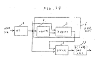
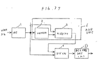
- Fig. 34 is a block diagram of an ac line frequency detection apparatus according to a sixteenth embodiment.
- the ac line frequency detection circuit has substantially the same structure as the illumination flicker detection apparatus according to the first embodiment. The difference is that an ac line frequency detection circuit 32 replaces the flicker judging circuit 5.
- the ac line frequency detection apparatus includes the integrating circuit 1, the averaging unit 6 including the memory 2 and the averaging circuit 3, the dividing circuit 4, and an ac line frequency detection circuit 32.
- a video signal is inputted to the integrating circuit 1.
- the integrating circuit 1 integrates pixel levels in every horizontal line (nit area) in a frame from the video signal.
- the memory 2 stores the integration result over a plurality of frames (fields).
- the averaging circuit 3 averages the integration results of horizontal lines at a plurality of frames (fields) from the integration result from the integrating circuit 1 and the memory 2.
- the dividing circuit 4 divides the integration results of horizontal lines by the averaged result of horizontal lines, respectively.
- the ac line frequency detection circuit 32 detects the frequency of an ac line voltage in accordance with the dividing results of horizontal lines.
- This ac line frequency detection apparatus is provided with a discrete circuit in this embodiment. However, the ac line frequency detection apparatus is also provided with a Digital Signal Processor (DSP), or a computer with a program.
- DSP Digital Signal Processor
- the video signal is generated by a video camera (not shown in Fig. 1) under illumination of which luminance varies in accordance with the voltage change of the ac line. That is, an image of an object, illuminated by fluorescent lamps, is shot by a video camera.
- the integration circuit 1 integrates, accumulates, or averages the pixel levels (luminance level) at every horizontal line.
- the memory 2 successively stores a predetermined number of frames (fields) of the integration results.
- the averaging circuit 3 effects addition or averaging among SUM n,i from the integration circuit 1, SUM n-1,i , SUM n-2,i , and SUM n-3,i from the memory 2.
- Fig. 2B shows the summing or averaging operation from the integration results of the present frame and the previous frames.
- the memory 2 stores the integration result SUM n,i and outputs the integration results SUM n-1,i , SUM n-2,i , SUM n-3,i at the i th line at frames n-1 to n-3.
- the averaging circuit 3 averages (sums) SUM ni , SUM n-1,i , SUM n-2,i , and SUM n-3,i .
- the averaging result is represented as AVE n,i .
- the number of the previous frames per one unit averaging operation is three.
- it is also possible that, at least, the integration results of more than one previous frames are added to the integration result of the present frame.
- the dividing circuit 4 obtains SUM n,i /AVE n,i through calculation from the output SUM n,i of the integration circuit 1 and the output AVE n,i of the averaging circuit 3a.
- the flicker judging circuit 5 judges whether there is flickering with the dividing result of the dividing circuit 4.
- the ac line frequency detection circuit 32 judges the existence of illumination flicker in the video signal generated with illumination using the ac line voltage and detects frequency of the ac line from the feature of the variation in the result of the dividing circuit 4. More specifically the ac line frequency detection circuit 32 detects the ac line frequency by analyzing the waveform of the variation in the result of the dividing circuit 4.
- Fig. 35 is a graphical drawing illustrating the ac line frequency operation according to the sixteenth embodiment.
- Fig. 36 depicts a flow chart showing the ac line frequency operation according to the sixteenth embodiment.
- the ac line frequency detection circuit 32 resets its count CNT to zero.
- the ac line frequency detection circuit 32 judges whether each of interval includes a half of lines corresponding to one cycle of flicker component to judge that the flicker frequency is developed by the ac line voltage of 50 Hz in steps 25 and 26.
- the theoretical number of the horizontal lines corresponding to one cycle of the flicker component is calculated from the frame frequency, the number of horizontal lines per frame, and the ac line frequency.
- step 26 the ac line frequency detection circuit 32 judges that the interval includes a half of horizontal lines corresponding to one cycle of the flicker component of 50 Hz when the number of horizontal lines lies within an allowable range from FREQ 50 MIN to FREQ 50 MAX to provide tolerance.
- the ac line frequency detection circuit 32 increments its count CNT in step s27 and processing returns to step s25 to repeat the operation in steps s25 to s27 for all lines in one frame.
- step s25 if all intervals of crossing points within one frame have been judged, processing proceeds to step s28.
- step s28 the ac line frequency detection circuit 32 compares the counts CNT with a threshold TH 4 in step s28. If the count CNT is higher than the threshold TH 4 , the ac line frequency detection circuit 32 judges that there is flicker of 50 Hz in this frame in step s29. If the count CNT is not higher than the threshold TH 4 , the ac line frequency detection circuit 32 judges that there is no flicker of 50 Hz in this frame in step s30 and detects that there is other flicker (for example, 60 Hz) as similar to the operation represented by steps s21 to s29.
- the ac line frequency detection circuit 32 compares the counts CNT with a threshold TH 4 in step s28. If the count CNT is higher than the threshold TH 4 , the ac line frequency detection circuit 32 judges that there is flicker of 50 Hz in this frame in step s29. If the count CNT is not higher than the threshold TH 4 , the ac line frequency detection circuit 32 judges that there is
- the ac line frequency detection circuit 32 After processing in steps s29 and s30, the ac line frequency detection circuit 32 returns to step s21 through the step s31 to repeat the above-mentioned operation of the next frame.
- the video levels of pixels at a frame of the video signal generated with illumination varying with the ac line voltage variation are integrated.
- the integrated results of frames, including the present frame, are averaged with respect to corresponding horizontal lines.
- the integration result of each line is divided by the averaging result of each line.
- the ac line frequency is judged from the frequency analyzing the variation in the dividing results.
- the ac line frequency measurement is possible without directly detecting the ac line voltage or ac current from an ac outlet.
- the ac line frequency is accurately measured without affection of luminance level variation due to movement of an object in the screen of the video signal.
- Fig. 37 is a block diagram of an ac line frequency detection apparatus according to a seventeenth embodiment.
- the ac line frequency detection apparatus has substantially the same structure as that according to the sixteenth embodiment. The difference is that an ac line frequency detection circuit 33 replaces the ac line frequency detection circuit 32.
- Fig. 38 is a block diagram of the ac line frequency detection circuit 33.
- the ac line frequency detection circuit 33 includes the DFT (Discrete Fourier Transform) circuit 21, supplied with the division result SUM n,i /AV n,i, for detecting frequency component levels and the comparing circuit 22 for comparing the output of the DFT circuit 21 with threshold values.
- DFT Discrete Fourier Transform
- the DFT circuit 21 supplied with the division result SUM n,i /AV n,i and the comparing circuit 22 for comparing the output of the DFT circuit 21 with threshold values.
- Fig. 4A shows the output of the dividing circuit 4, wherein the axis of abscissas represents line number at a frame and the axis of ordinates represents levels of dividing results, that is, SUM n,i /AV n,i .
- the dividing results shows flicker.
- Fig. 4B shows the output of the DFT circuit 21, wherein the axis of abscissas represents frequency and axis of ordinates represents levels of frequency components.
- the DFT circuit 21 effects Discrete Fourier Transform operation to output frequency components as shown in Fig. 4B from the division result of the division circuit 4.
- the line F 50 represents the level of the DFT circuit 21 at 50 Hz, i.e., component of 50 Hz and the line F60 represents the level of the DFT circuit 21 at 60 Hz, i.e., component of 60 Hz.
- the comparing circuit 22 compares the results F50 and F 60 of the DFT circuit 21 with threshold levels TH 50-ON , TH 60-ON , TH 50-OFF , and TH 60-OFF . There are relations, TH 50-ON > TH 50-OFF and TH 60-ON > TH 60-OFF .
- the comparing circuit 22 compares the component F50 with the threshold levels TH 50-ON and TH 50-OFF and the component F60 with the threshold levels TH 60-ON and TH 60-OFF to detect flicker in the video signal.
- the comparing circuit 22 judges the flicker as follows:
- the comparing circuit 22 judges there is flicker of 50 Hz.
- the comparing circuit 22 judges there is flicker of 60 Hz.
- the comparing circuit 22 judges that it is unknown that there is flicker.
- ⁇ is a weighting coefficient for flicker detection of 50 Hz and ⁇ is a weighting coefficient for flicker detection of 60 Hz. These coefficients are sufficiently greater than one, so that if the frequency component F 50 (F 60 ) is greater than the value of the weighting-coefficient-times the frequency component F 60 (F 50 ), the comparing circuit 22 judges there is flicker of 50 Hz (60 Hz). This reduces probability of erroneous judgment of existence of flicker due to luminance level change within a frame representing an image.
- the existence of flicker is judged from the average of integration values over a plurality of frames (fields) including the present frame at the corresponding lines.
- the flicker detection can be provided without affection of luminance level variation due to motion of the image.
- this structure (this method) provides illumination flicker detection of 60 Hz wherein luminance level variation.
- the integration circuit 1 integrates the pixel values every horizontal line.
- the integration circuit 1 integrates the pixel value on thinned horizontal lines, wherein thinning period is sufficiently shorter than the period of flicker (beat) component.
- the circuit stage after the integration circuit 1 effects the above-mentioned operation for the thinned horizontal lines.
- the capacity of the memory 2b can be reduced.
- the ac line frequency detection apparatus includes the DFT circuit 21 and the comparing circuit 22, so that the presence of illumination flicker at one of various ac line frequencies can be detected substantially at the same time.
- Fig. 39 is an ac line frequency detection apparatus according to an eighteenth embodiment.
- the ac line frequency detection apparatus according to the eighteenth embodiment has substantially the same structure as that according to the sixteenth embodiment or the seventeenth embodiment.
- the difference is that an imaging circuit 200 is further provided.
- the imaging circuit 200 includes an imaging element and a driving circuit (not shown).
- the imaging circuit 200 generates and supplies the video signal to the integrating circuit 1.
- the memory 2, the averaging circuit 3, dividing circuit 4, and the ac line frequency detection circuit 32 (33) detect ac line frequency as mentioned above.
- the ac line frequency detection apparatus can indirectly detect the existence of illumination flicker and the frequency of the illumination flicker from the image without directly detecting the ac line voltage or ac line current from the ac outlet. Moreover, because the ac line frequency detection apparatus according to the eighteenth embodiment includes the imaging circuit, so that there is no necessity of a unit generating the video signal and the cable for supplying the video signal to the integrating circuit 1.
Landscapes
- Engineering & Computer Science (AREA)
- Multimedia (AREA)
- Signal Processing (AREA)
- Picture Signal Circuits (AREA)
- Transforming Light Signals Into Electric Signals (AREA)
- Studio Devices (AREA)
Applications Claiming Priority (6)
| Application Number | Priority Date | Filing Date | Title |
|---|---|---|---|
| JP28831099 | 1999-10-08 | ||
| JP28831099A JP3539901B2 (ja) | 1999-10-08 | 1999-10-08 | フリッカ検出・補正装置およびフリッカ検出・補正方法 |
| JP29731699A JP3476400B2 (ja) | 1999-10-19 | 1999-10-19 | フリッカ検出・補正装置およびフリッカ検出・補正方法 |
| JP29731699 | 1999-10-19 | ||
| JP32443699 | 1999-11-15 | ||
| JP32443699A JP2001141763A (ja) | 1999-11-15 | 1999-11-15 | 電源周波数測定装置および方法 |
Publications (3)
| Publication Number | Publication Date |
|---|---|
| EP1091571A2 true EP1091571A2 (de) | 2001-04-11 |
| EP1091571A3 EP1091571A3 (de) | 2002-10-16 |
| EP1091571B1 EP1091571B1 (de) | 2012-05-30 |
Family
ID=27337433
Family Applications (1)
| Application Number | Title | Priority Date | Filing Date |
|---|---|---|---|
| EP00308844A Expired - Lifetime EP1091571B1 (de) | 1999-10-08 | 2000-10-06 | Vorrichtungen und Verfahren zur Erkennung und Kompensation von Beleuchtungsflimmern, Erkennung und Messung der Netzfrequenz |
Country Status (4)
| Country | Link |
|---|---|
| US (1) | US6710818B1 (de) |
| EP (1) | EP1091571B1 (de) |
| CN (1) | CN1156152C (de) |
| CA (1) | CA2322593C (de) |
Cited By (12)
| Publication number | Priority date | Publication date | Assignee | Title |
|---|---|---|---|---|
| EP1253780A2 (de) | 2001-04-26 | 2002-10-30 | Fujitsu Limited | Flimmerrauschreduzierungsverfahren für X-Y addressierte Festkörperbildaufnehmer |
| WO2004032483A3 (de) * | 2002-10-01 | 2004-05-06 | Bayerische Motoren Werke Ag | Verfahren zum betreiben einer optoelektronischen sensorvorrichtung |
| WO2004047427A1 (ja) | 2002-11-18 | 2004-06-03 | Sony Corporation | フリッカ低減方法、撮像装置およびフリッカ低減回路 |
| EP1324598A3 (de) * | 2001-12-27 | 2005-05-25 | Sharp Kabushiki Kaisha | Flimmerkorrekturvorrichtung, -methode und Aufnahmemedium zur Speicherung eines Flimmerkorrekturprograms |
| EP1732313A1 (de) * | 2005-06-10 | 2006-12-13 | Sony Corporation | Bildverarbeitungsvorrichtung und Bildaufnahmevorrichtung |
| EP1898636A2 (de) | 2006-09-07 | 2008-03-12 | Sony Corporation | Vorrichtung und Verfahren zur Bilddatenverarbeitung und Abbildungssystem |
| WO2008108025A1 (en) * | 2007-03-05 | 2008-09-12 | Nec Electronics Corporation | Imaging apparatus and flicker detection method |
| EP1679906A4 (de) * | 2003-10-31 | 2009-09-02 | Mitsubishi Electric Corp | Bilderfassungseinrichtung |
| EP2695373A4 (de) * | 2011-04-06 | 2014-11-12 | Pelco Inc | Flackererkennung mit räumlicher varianz |
| US8903171B2 (en) | 2009-06-09 | 2014-12-02 | Google Inc. | Detection and suppression of flicker in a sequence of images |
| EP2827579A1 (de) * | 2013-07-19 | 2015-01-21 | Fujitsu Limited | Flackerdetektionsverfahren und Flackerdetektionsvorrichtung |
| DE102014007401A1 (de) * | 2014-05-20 | 2015-11-26 | Schölly Fiberoptic GmbH | Verfahren zur Bildaufnahme einer stroboskopisch beleuchteten Szene und Bildaufnahmevorrichtung |
Families Citing this family (87)
| Publication number | Priority date | Publication date | Assignee | Title |
|---|---|---|---|---|
| JP3375557B2 (ja) * | 1999-01-29 | 2003-02-10 | 松下電器産業株式会社 | 映像信号処理装置 |
| JP3370979B2 (ja) * | 2000-09-08 | 2003-01-27 | 三菱電機株式会社 | 撮像装置および自動レベル調整方法 |
| JP2003018458A (ja) * | 2001-04-23 | 2003-01-17 | Hitachi Ltd | Cmos型固体撮像素子を用いた撮像システム |
| AU2002305780A1 (en) * | 2001-05-29 | 2002-12-09 | Transchip, Inc. | Patent application cmos imager for cellular applications and methods of using such |
| US7738013B2 (en) * | 2001-05-29 | 2010-06-15 | Samsung Electronics Co., Ltd. | Systems and methods for power conservation in a CMOS imager |
| JP4759877B2 (ja) * | 2001-08-10 | 2011-08-31 | コニカミノルタビジネステクノロジーズ株式会社 | 画像処理プログラム及びその記録媒体、画像処理方法並びに画像処理装置 |
| US7298401B2 (en) * | 2001-08-10 | 2007-11-20 | Micron Technology, Inc. | Method and apparatus for removing flicker from images |
| JP3823314B2 (ja) * | 2001-12-18 | 2006-09-20 | ソニー株式会社 | 撮像信号処理装置及びフリッカ検出方法 |
| JP3928424B2 (ja) * | 2001-12-26 | 2007-06-13 | コニカミノルタビジネステクノロジーズ株式会社 | 動画におけるフリッカ補正 |
| JP4337353B2 (ja) * | 2002-03-25 | 2009-09-30 | セイコーエプソン株式会社 | フリッカ検出装置、フリッカ補正装置、撮像装置、フリッカ検出プログラムおよびフリッカ補正プログラム |
| US6995774B2 (en) * | 2002-07-10 | 2006-02-07 | L3 Communications Corporation | Display system and method of diminishing unwanted artifacts |
| JP2004112739A (ja) * | 2002-07-25 | 2004-04-08 | Fujitsu Ltd | 固体イメージセンサ |
| JP3803924B2 (ja) * | 2002-09-09 | 2006-08-02 | 本田技研工業株式会社 | イメージセンサ |
| JP2004112034A (ja) * | 2002-09-13 | 2004-04-08 | Canon Inc | 撮像装置 |
| KR100460755B1 (ko) * | 2002-10-10 | 2004-12-14 | 매그나칩 반도체 유한회사 | 이미지센서의 화소배열부 및 그를 포함하는 이미지센서 및이미지센서의 플리커 잡음 제거방법 |
| US7126639B2 (en) * | 2002-10-29 | 2006-10-24 | Hewlett-Packard Development Company, L.P. | Digital camera printing user interface responsive to location |
| JPWO2004091194A1 (ja) * | 2003-04-09 | 2006-07-06 | 三菱電機株式会社 | 撮像装置 |
| US7068446B2 (en) * | 2003-05-05 | 2006-06-27 | Illumitech Inc. | Compact non-imaging light collector |
| JP3826904B2 (ja) * | 2003-07-08 | 2006-09-27 | ソニー株式会社 | 撮像装置およびフリッカ低減方法 |
| US7397503B2 (en) * | 2003-07-28 | 2008-07-08 | Micron Technology, Inc. | Systems and methods for reducing artifacts caused by illuminant flicker |
| JP4106554B2 (ja) * | 2003-09-08 | 2008-06-25 | ソニー株式会社 | 撮影環境判定方法および撮像装置 |
| KR100552969B1 (ko) * | 2003-09-29 | 2006-02-15 | 삼성에스디아이 주식회사 | 필드순차구동방식의 액정표시장치 |
| JP4331026B2 (ja) * | 2004-03-17 | 2009-09-16 | 富士通マイクロエレクトロニクス株式会社 | フリッカノイズ検出方法、フリッカノイズ低減方法及びフリッカノイズ検出回路 |
| KR100574890B1 (ko) * | 2004-04-27 | 2006-04-27 | 매그나칩 반도체 유한회사 | 이미지센서 및 이미지센서의 플리커 노이즈 검출 방법 |
| US7502054B2 (en) * | 2004-12-20 | 2009-03-10 | Pixim, Inc. | Automatic detection of fluorescent flicker in video images |
| JP4377840B2 (ja) * | 2005-03-31 | 2009-12-02 | イーストマン コダック カンパニー | デジタルカメラ |
| JP4453648B2 (ja) * | 2005-06-13 | 2010-04-21 | ソニー株式会社 | 画像処理装置および撮像装置 |
| JP4631611B2 (ja) * | 2005-08-30 | 2011-02-16 | ソニー株式会社 | フリッカ検出装置とフリッカ除去装置と撮像装置およびフリッカ検出方法 |
| JP4904749B2 (ja) * | 2005-09-08 | 2012-03-28 | ソニー株式会社 | フリッカ低減方法、フリッカ低減回路及び撮像装置 |
| US7598987B2 (en) * | 2005-11-29 | 2009-10-06 | Stmicroelectronics Asia Pacific Pte. Ltd. | Flicker detection gain control circuit, digital imaging system, and method |
| US8068148B2 (en) * | 2006-01-05 | 2011-11-29 | Qualcomm Incorporated | Automatic flicker correction in an image capture device |
| TWI311883B (en) * | 2006-05-10 | 2009-07-01 | Novatek Microelectronics Corp | Flicker frequency detection method and device |
| CN100420271C (zh) * | 2006-06-13 | 2008-09-17 | 北京中星微电子有限公司 | 一种图像序列帧间闪烁噪声消除装置 |
| CN100420270C (zh) * | 2006-06-13 | 2008-09-17 | 北京中星微电子有限公司 | 图像序列帧间闪烁噪声消除方法 |
| JP4969336B2 (ja) * | 2006-10-06 | 2012-07-04 | 日立オムロンターミナルソリューションズ株式会社 | カメラおよびカメラを用いた監視装置 |
| JP2009004845A (ja) * | 2007-06-19 | 2009-01-08 | Panasonic Corp | 撮像装置、撮像方法、プログラム、および集積回路 |
| US8081235B2 (en) * | 2007-11-12 | 2011-12-20 | Canon Kabushiki Kaisha | Image pickup apparatus and flicker detection method therefor |
| JP4971956B2 (ja) * | 2007-11-27 | 2012-07-11 | キヤノン株式会社 | フリッカ補正装置、フリッカ補正方法並びに撮像装置 |
| JP5111100B2 (ja) * | 2007-12-28 | 2012-12-26 | キヤノン株式会社 | 画像処理装置、画像処理方法、プログラム及び記憶媒体 |
| CN101582992B (zh) * | 2008-05-15 | 2012-12-19 | 鸿富锦精密工业(深圳)有限公司 | 闪烁消除系统及消除闪烁的方法 |
| CN101600045B (zh) * | 2008-06-03 | 2010-12-29 | 联咏科技股份有限公司 | 信号调节电路及其视频装置 |
| US7911505B2 (en) * | 2008-08-20 | 2011-03-22 | Eastman Kodak Company | Detecting illuminant flicker |
| JP4626689B2 (ja) * | 2008-08-26 | 2011-02-09 | ソニー株式会社 | 撮像装置、補正回路および補正方法 |
| US8194152B2 (en) * | 2008-09-05 | 2012-06-05 | CSR Technology, Inc. | Image processing under flickering lighting conditions using estimated illumination parameters |
| JP2010114674A (ja) * | 2008-11-06 | 2010-05-20 | Sanyo Electric Co Ltd | ビデオカメラ |
| US8441551B2 (en) * | 2008-11-14 | 2013-05-14 | Ati Technologies Ulc | Flicker detection circuit for imaging sensors that employ rolling shutters |
| WO2010058567A1 (ja) * | 2008-11-20 | 2010-05-27 | パナソニック株式会社 | フリッカ低減装置、集積回路及びフリッカ低減方法 |
| JP5218239B2 (ja) * | 2009-04-14 | 2013-06-26 | ソニー株式会社 | 画像データ処理装置および撮像装置 |
| JP2011030093A (ja) * | 2009-07-28 | 2011-02-10 | Sanyo Electric Co Ltd | ビデオカメラ |
| JP2011091775A (ja) | 2009-10-26 | 2011-05-06 | Toshiba Corp | 固体撮像装置 |
| CN102118549B (zh) * | 2009-12-31 | 2013-02-27 | 敦南科技股份有限公司 | 影像感测装置检测闪频光的方法及其影像感测装置 |
| US8441549B2 (en) * | 2010-02-03 | 2013-05-14 | Microsoft Corporation | Video artifact suppression via rolling flicker detection |
| US8390701B2 (en) * | 2010-04-29 | 2013-03-05 | Robert Bosch Gmbh | Method for processing an image signal for double or multiple exposure cameras |
| JP5634901B2 (ja) * | 2010-05-10 | 2014-12-03 | パナソニック株式会社 | 撮像装置、外部閃光補正方法、プログラム、および、集積回路 |
| JP5644451B2 (ja) * | 2010-05-25 | 2014-12-24 | 株式会社リコー | 画像処理装置および画像処理方法、ならびに、撮像装置 |
| JP5331766B2 (ja) * | 2010-09-03 | 2013-10-30 | 株式会社日立製作所 | 撮像装置 |
| US8462229B2 (en) * | 2010-09-30 | 2013-06-11 | Hewlett-Packard Development Company, L.P. | Detection of flicker within captured imaged frames |
| CN101977285B (zh) * | 2010-11-29 | 2015-09-02 | 杭州海康威视数字技术股份有限公司 | 摄像系统和摄像方法 |
| CN102103267A (zh) * | 2011-01-20 | 2011-06-22 | 深圳市艾讴科技有限公司 | 一种快门眼镜及其调节方法 |
| US8711245B2 (en) * | 2011-03-18 | 2014-04-29 | Digitaloptics Corporation Europe Ltd. | Methods and systems for flicker correction |
| JP2013003238A (ja) * | 2011-06-14 | 2013-01-07 | Sony Corp | 映像信号処理回路、映像信号処理方法、表示装置、及び、電子機器 |
| US9418115B2 (en) | 2011-07-26 | 2016-08-16 | Abl Ip Holding Llc | Location-based mobile services and applications |
| US8334898B1 (en) | 2011-07-26 | 2012-12-18 | ByteLight, Inc. | Method and system for configuring an imaging device for the reception of digital pulse recognition information |
| US9787397B2 (en) | 2011-07-26 | 2017-10-10 | Abl Ip Holding Llc | Self identifying modulated light source |
| US8248467B1 (en) | 2011-07-26 | 2012-08-21 | ByteLight, Inc. | Light positioning system using digital pulse recognition |
| US9723676B2 (en) | 2011-07-26 | 2017-08-01 | Abl Ip Holding Llc | Method and system for modifying a beacon light source for use in a light based positioning system |
| EP3119164B8 (de) | 2011-07-26 | 2019-12-11 | ABL IP Holding LLC | Selbstidentifizierende modulator-lichtquelle |
| US9287976B2 (en) | 2011-07-26 | 2016-03-15 | Abl Ip Holding Llc | Independent beacon based light position system |
| US9444547B2 (en) | 2011-07-26 | 2016-09-13 | Abl Ip Holding Llc | Self-identifying one-way authentication method using optical signals |
| US8416290B2 (en) | 2011-07-26 | 2013-04-09 | ByteLight, Inc. | Method and system for digital pulse recognition demodulation |
| TWI469632B (zh) * | 2011-11-09 | 2015-01-11 | Silicon Motion Inc | 抗閃爍攝錄裝置與攝錄方法 |
| WO2014167865A1 (ja) * | 2013-04-12 | 2014-10-16 | パナソニック インテレクチュアル プロパティ コーポレーション オブ アメリカ | フリッカ低減装置、撮像装置およびフリッカ低減方法 |
| CN104166045B (zh) * | 2013-05-15 | 2016-12-28 | 海洋王(东莞)照明科技有限公司 | 一种交流电源频率检测装置 |
| US9705600B1 (en) | 2013-06-05 | 2017-07-11 | Abl Ip Holding Llc | Method and system for optical communication |
| US9900092B2 (en) * | 2013-07-23 | 2018-02-20 | Philips Lighting Holding B.V. | Modulation of coded light components |
| WO2015077767A1 (en) | 2013-11-25 | 2015-05-28 | Daniel Ryan | System and method for communication with a mobile device via a positioning system including rf communication devices and modulated beacon light sources |
| US9686505B2 (en) | 2014-01-03 | 2017-06-20 | Mediatek Singapore Pte. Ltd. | Method for flicker detection and associated circuit |
| EP2950523A1 (de) * | 2014-05-28 | 2015-12-02 | Thomson Licensing | Verfahren zur Schätzung des Flimmerns auf einem mit einem Camcorder aufgezeichnete Video |
| EP3487192A1 (de) | 2014-08-12 | 2019-05-22 | ABL IP Holding LLC | System und verfahren zur schätzung der position und ausrichtung einer mobilkommunikationsvorrichtung in einem bakenbasierten positionierungssystem |
| US9584704B2 (en) * | 2015-01-08 | 2017-02-28 | Gean Technology Co. Limited | Method for detecting electronic lighting flickering |
| KR20170111460A (ko) * | 2016-03-28 | 2017-10-12 | 삼성전자주식회사 | 카메라를 통해 획득한 영상 처리 방법 및 장치전자 장치 |
| WO2018211511A1 (en) * | 2017-05-16 | 2018-11-22 | Technion Research & Development Foundation Limited | Computational imaging of the electric grid |
| KR102686100B1 (ko) * | 2019-07-18 | 2024-07-19 | 삼성디스플레이 주식회사 | 표시 패널의 구동 방법 및 이를 수행하기 위한 표시 장치 |
| CN111487257A (zh) * | 2020-04-01 | 2020-08-04 | 武汉精立电子技术有限公司 | 一种显示面板异常像素实时检测修复方法及装置 |
| EP4274207A4 (de) | 2021-04-13 | 2024-07-10 | Samsung Electronics Co., Ltd. | Elektronische vorrichtung und steuerungsverfahren dafür |
| JP7838315B2 (ja) | 2022-03-02 | 2026-04-01 | 株式会社ソシオネクスト | 撮像装置および画像処理装置 |
| KR20240018726A (ko) * | 2022-08-02 | 2024-02-14 | 삼성디스플레이 주식회사 | 표시 장치 |
Citations (2)
| Publication number | Priority date | Publication date | Assignee | Title |
|---|---|---|---|---|
| US5384595A (en) | 1990-04-19 | 1995-01-24 | Matsushita Electric Industrial Co., Ltd. | Motion detector and image stabilizing system |
| EP0762742A2 (de) | 1995-08-29 | 1997-03-12 | Canon Kabushiki Kaisha | Videokamera mit auswechselbarer Linsenvorrichtung |
Family Cites Families (10)
| Publication number | Priority date | Publication date | Assignee | Title |
|---|---|---|---|---|
| JPS62134567A (ja) | 1985-12-09 | 1987-06-17 | Matsushita Electric Ind Co Ltd | 電源周波数判別装置 |
| JPS63105580A (ja) * | 1986-10-22 | 1988-05-10 | Hitachi Ltd | テレビカメラ |
| JPH0815324B2 (ja) * | 1987-06-10 | 1996-02-14 | キヤノン株式会社 | テレビ用固体撮像装置 |
| JPH02252371A (ja) * | 1989-03-24 | 1990-10-11 | Fujitsu General Ltd | Ccdカメラのオートフリッカレス回路 |
| JPH031791A (ja) * | 1989-05-30 | 1991-01-08 | Sony Corp | オートホワイトバランス回路 |
| JPH06303465A (ja) * | 1993-04-16 | 1994-10-28 | Mitsubishi Electric Corp | 画像のフリッカ補正回路 |
| US5501518A (en) * | 1994-01-31 | 1996-03-26 | Dell Usa, L.P. | Hand-held keyboard tester |
| JP3405822B2 (ja) | 1994-06-28 | 2003-05-12 | ローム株式会社 | クロスコイルメータ |
| JPH08265652A (ja) * | 1995-03-20 | 1996-10-11 | Fujitsu General Ltd | Ccdカメラ装置 |
| US6295085B1 (en) * | 1997-12-08 | 2001-09-25 | Intel Corporation | Method and apparatus for eliminating flicker effects from discharge lamps during digital video capture |
-
2000
- 2000-10-06 US US09/680,216 patent/US6710818B1/en not_active Expired - Fee Related
- 2000-10-06 CA CA002322593A patent/CA2322593C/en not_active Expired - Fee Related
- 2000-10-06 CN CNB001306359A patent/CN1156152C/zh not_active Expired - Fee Related
- 2000-10-06 EP EP00308844A patent/EP1091571B1/de not_active Expired - Lifetime
Patent Citations (2)
| Publication number | Priority date | Publication date | Assignee | Title |
|---|---|---|---|---|
| US5384595A (en) | 1990-04-19 | 1995-01-24 | Matsushita Electric Industrial Co., Ltd. | Motion detector and image stabilizing system |
| EP0762742A2 (de) | 1995-08-29 | 1997-03-12 | Canon Kabushiki Kaisha | Videokamera mit auswechselbarer Linsenvorrichtung |
Cited By (25)
| Publication number | Priority date | Publication date | Assignee | Title |
|---|---|---|---|---|
| EP1921846A3 (de) * | 2001-04-26 | 2012-05-16 | Fujitsu Semiconductor Limited | Flimmerrauschreduzierungsverfahren für X-Y addressierte Festkörperbildaufnehmer |
| EP1253780A3 (de) * | 2001-04-26 | 2004-01-21 | Fujitsu Limited | Flimmerrauschreduzierungsverfahren für X-Y addressierte Festkörperbildaufnehmer |
| US7106368B2 (en) | 2001-04-26 | 2006-09-12 | Fujitsu Limited | Method of reducing flicker noises of X-Y address type solid-state image pickup device |
| EP1253780A2 (de) | 2001-04-26 | 2002-10-30 | Fujitsu Limited | Flimmerrauschreduzierungsverfahren für X-Y addressierte Festkörperbildaufnehmer |
| EP1324598A3 (de) * | 2001-12-27 | 2005-05-25 | Sharp Kabushiki Kaisha | Flimmerkorrekturvorrichtung, -methode und Aufnahmemedium zur Speicherung eines Flimmerkorrekturprograms |
| US7164439B2 (en) | 2001-12-27 | 2007-01-16 | Sharp Kabushiki Kaisha | Flicker correction apparatus and flicker correction method, and recording medium storing flicker correction program |
| WO2004032483A3 (de) * | 2002-10-01 | 2004-05-06 | Bayerische Motoren Werke Ag | Verfahren zum betreiben einer optoelektronischen sensorvorrichtung |
| US7151259B2 (en) | 2002-10-01 | 2006-12-19 | Bayerische Motoren Werke Aktiengesellschaft | Method for operating an optoelectronic sensor device |
| WO2004047427A1 (ja) | 2002-11-18 | 2004-06-03 | Sony Corporation | フリッカ低減方法、撮像装置およびフリッカ低減回路 |
| US7656436B2 (en) | 2002-11-18 | 2010-02-02 | Sony Corporation | Flicker reduction method, image pickup device, and flicker reduction circuit |
| EP1566962A4 (de) * | 2002-11-18 | 2009-09-16 | Sony Corp | Flackerverringerungsverfahren, bilderfassungseinrichtung und flackerverringerungsschaltung |
| US7683941B2 (en) | 2003-10-31 | 2010-03-23 | Mitsubishi Denki Kabushiki Kaisha | Image pickup apparatus |
| EP1679906A4 (de) * | 2003-10-31 | 2009-09-02 | Mitsubishi Electric Corp | Bilderfassungseinrichtung |
| EP1732313A1 (de) * | 2005-06-10 | 2006-12-13 | Sony Corporation | Bildverarbeitungsvorrichtung und Bildaufnahmevorrichtung |
| EP1898636A3 (de) * | 2006-09-07 | 2011-08-24 | Sony Corporation | Vorrichtung und Verfahren zur Bilddatenverarbeitung und Abbildungssystem |
| EP1898636A2 (de) | 2006-09-07 | 2008-03-12 | Sony Corporation | Vorrichtung und Verfahren zur Bilddatenverarbeitung und Abbildungssystem |
| WO2008108025A1 (en) * | 2007-03-05 | 2008-09-12 | Nec Electronics Corporation | Imaging apparatus and flicker detection method |
| US8279303B2 (en) | 2007-03-05 | 2012-10-02 | Renesas Electronics Corporation | Imaging apparatus and flicker detection method |
| US8903171B2 (en) | 2009-06-09 | 2014-12-02 | Google Inc. | Detection and suppression of flicker in a sequence of images |
| EP2695373A4 (de) * | 2011-04-06 | 2014-11-12 | Pelco Inc | Flackererkennung mit räumlicher varianz |
| US9088727B2 (en) | 2011-04-06 | 2015-07-21 | Pelco, Inc. | Spatially-varying flicker detection |
| EP2827579A1 (de) * | 2013-07-19 | 2015-01-21 | Fujitsu Limited | Flackerdetektionsverfahren und Flackerdetektionsvorrichtung |
| US9148583B2 (en) | 2013-07-19 | 2015-09-29 | Fujitsu Limited | Flicker detection method and flicker detection apparatus |
| DE102014007401A1 (de) * | 2014-05-20 | 2015-11-26 | Schölly Fiberoptic GmbH | Verfahren zur Bildaufnahme einer stroboskopisch beleuchteten Szene und Bildaufnahmevorrichtung |
| DE102014007401B4 (de) | 2014-05-20 | 2021-10-14 | Schölly Fiberoptic GmbH | Verfahren zur Bildaufnahme einer stroboskopisch beleuchteten Szene und Bildaufnahmevorrichtung |
Also Published As
| Publication number | Publication date |
|---|---|
| CA2322593A1 (en) | 2001-04-08 |
| CN1156152C (zh) | 2004-06-30 |
| CA2322593C (en) | 2004-02-03 |
| US6710818B1 (en) | 2004-03-23 |
| EP1091571A3 (de) | 2002-10-16 |
| CN1292623A (zh) | 2001-04-25 |
| EP1091571B1 (de) | 2012-05-30 |
Similar Documents
| Publication | Publication Date | Title |
|---|---|---|
| US6710818B1 (en) | Illumination flicker detection apparatus, an illumination flicker compensation apparatus, and an ac line frequency detection apparatus, methods of detecting illumination flicker, compensating illumination flicker, and measuring ac line frequency | |
| KR101040842B1 (ko) | 플리커 저감 방법, 촬상 장치 및 플리커 저감 회로 | |
| KR101007427B1 (ko) | 촬상 장치 및 플리커 저감 방법 | |
| US8115828B2 (en) | Image processing apparatus, flicker reduction method, imaging apparatus, and flicker reduction program | |
| KR101007464B1 (ko) | 촬영 환경 판정 방법 및 촬상 장치 | |
| JP4487640B2 (ja) | 撮像装置 | |
| US8031237B2 (en) | Exposure control method, exposure control apparatus and image pickup apparatus | |
| JP4904749B2 (ja) | フリッカ低減方法、フリッカ低減回路及び撮像装置 | |
| JP3539901B2 (ja) | フリッカ検出・補正装置およびフリッカ検出・補正方法 | |
| JP3476400B2 (ja) | フリッカ検出・補正装置およびフリッカ検出・補正方法 | |
| KR20060128649A (ko) | 화상 처리 장치 및 촬상 장치 | |
| US6768511B1 (en) | Exposure control circuit for solid-state imaging apparatus |
Legal Events
| Date | Code | Title | Description |
|---|---|---|---|
| PUAI | Public reference made under article 153(3) epc to a published international application that has entered the european phase |
Free format text: ORIGINAL CODE: 0009012 |
|
| AK | Designated contracting states |
Kind code of ref document: A2 Designated state(s): AT BE CH CY DE DK ES FI FR GB GR IE IT LI LU MC NL PT SE |
|
| AX | Request for extension of the european patent |
Free format text: AL;LT;LV;MK;RO;SI |
|
| PUAL | Search report despatched |
Free format text: ORIGINAL CODE: 0009013 |
|
| AK | Designated contracting states |
Kind code of ref document: A3 Designated state(s): AT BE CH CY DE DK ES FI FR GB GR IE IT LI LU MC NL PT SE |
|
| AX | Request for extension of the european patent |
Free format text: AL;LT;LV;MK;RO;SI |
|
| RIC1 | Information provided on ipc code assigned before grant |
Free format text: 7H 04N 5/235 A, 7H 04N 5/243 B, 7H 04N 5/217 B |
|
| 17P | Request for examination filed |
Effective date: 20021213 |
|
| AKX | Designation fees paid |
Designated state(s): DE FR GB NL |
|
| 17Q | First examination report despatched |
Effective date: 20060828 |
|
| RAP1 | Party data changed (applicant data changed or rights of an application transferred) |
Owner name: PANASONIC CORPORATION |
|
| GRAP | Despatch of communication of intention to grant a patent |
Free format text: ORIGINAL CODE: EPIDOSNIGR1 |
|
| GRAS | Grant fee paid |
Free format text: ORIGINAL CODE: EPIDOSNIGR3 |
|
| GRAA | (expected) grant |
Free format text: ORIGINAL CODE: 0009210 |
|
| AK | Designated contracting states |
Kind code of ref document: B1 Designated state(s): DE FR GB NL |
|
| REG | Reference to a national code |
Ref country code: GB Ref legal event code: FG4D |
|
| REG | Reference to a national code |
Ref country code: DE Ref legal event code: R096 Ref document number: 60047225 Country of ref document: DE Effective date: 20120802 |
|
| REG | Reference to a national code |
Ref country code: NL Ref legal event code: VDEP Effective date: 20120530 |
|
| PG25 | Lapsed in a contracting state [announced via postgrant information from national office to epo] |
Ref country code: NL Free format text: LAPSE BECAUSE OF FAILURE TO SUBMIT A TRANSLATION OF THE DESCRIPTION OR TO PAY THE FEE WITHIN THE PRESCRIBED TIME-LIMIT Effective date: 20120530 |
|
| PLBE | No opposition filed within time limit |
Free format text: ORIGINAL CODE: 0009261 |
|
| STAA | Information on the status of an ep patent application or granted ep patent |
Free format text: STATUS: NO OPPOSITION FILED WITHIN TIME LIMIT |
|
| 26N | No opposition filed |
Effective date: 20130301 |
|
| REG | Reference to a national code |
Ref country code: DE Ref legal event code: R097 Ref document number: 60047225 Country of ref document: DE Effective date: 20130301 |
|
| REG | Reference to a national code |
Ref country code: FR Ref legal event code: ST Effective date: 20130628 |
|
| PG25 | Lapsed in a contracting state [announced via postgrant information from national office to epo] |
Ref country code: FR Free format text: LAPSE BECAUSE OF NON-PAYMENT OF DUE FEES Effective date: 20121031 |
|
| PGFP | Annual fee paid to national office [announced via postgrant information from national office to epo] |
Ref country code: GB Payment date: 20131021 Year of fee payment: 14 Ref country code: DE Payment date: 20131021 Year of fee payment: 14 |
|
| REG | Reference to a national code |
Ref country code: GB Ref legal event code: 746 Effective date: 20140703 |
|
| REG | Reference to a national code |
Ref country code: DE Ref legal event code: R084 Ref document number: 60047225 Country of ref document: DE Effective date: 20140620 |
|
| REG | Reference to a national code |
Ref country code: DE Ref legal event code: R119 Ref document number: 60047225 Country of ref document: DE |
|
| GBPC | Gb: european patent ceased through non-payment of renewal fee |
Effective date: 20141006 |
|
| PG25 | Lapsed in a contracting state [announced via postgrant information from national office to epo] |
Ref country code: GB Free format text: LAPSE BECAUSE OF NON-PAYMENT OF DUE FEES Effective date: 20141006 Ref country code: DE Free format text: LAPSE BECAUSE OF NON-PAYMENT OF DUE FEES Effective date: 20150501 |