EP1092755A1 - Composition pour revetement - Google Patents
Composition pour revetement Download PDFInfo
- Publication number
- EP1092755A1 EP1092755A1 EP00912922A EP00912922A EP1092755A1 EP 1092755 A1 EP1092755 A1 EP 1092755A1 EP 00912922 A EP00912922 A EP 00912922A EP 00912922 A EP00912922 A EP 00912922A EP 1092755 A1 EP1092755 A1 EP 1092755A1
- Authority
- EP
- European Patent Office
- Prior art keywords
- silicon
- solvent
- coating composition
- film
- compound
- Prior art date
- Legal status (The legal status is an assumption and is not a legal conclusion. Google has not performed a legal analysis and makes no representation as to the accuracy of the status listed.)
- Withdrawn
Links
Images

Classifications
-
- H—ELECTRICITY
- H10—SEMICONDUCTOR DEVICES; ELECTRIC SOLID-STATE DEVICES NOT OTHERWISE PROVIDED FOR
- H10P—GENERIC PROCESSES OR APPARATUS FOR THE MANUFACTURE OR TREATMENT OF DEVICES COVERED BY CLASS H10
- H10P14/00—Formation of materials, e.g. in the shape of layers or pillars
- H10P14/20—Formation of materials, e.g. in the shape of layers or pillars of semiconductor materials
- H10P14/34—Deposited materials, e.g. layers
- H10P14/3438—Doping during depositing
- H10P14/3441—Conductivity type
-
- B—PERFORMING OPERATIONS; TRANSPORTING
- B05—SPRAYING OR ATOMISING IN GENERAL; APPLYING FLUENT MATERIALS TO SURFACES, IN GENERAL
- B05D—PROCESSES FOR APPLYING FLUENT MATERIALS TO SURFACES, IN GENERAL
- B05D3/00—Pretreatment of surfaces to which liquids or other fluent materials are to be applied; After-treatment of applied coatings, e.g. intermediate treating of an applied coating preparatory to subsequent applications of liquids or other fluent materials
- B05D3/06—Pretreatment of surfaces to which liquids or other fluent materials are to be applied; After-treatment of applied coatings, e.g. intermediate treating of an applied coating preparatory to subsequent applications of liquids or other fluent materials by exposure to radiation
- B05D3/061—Pretreatment of surfaces to which liquids or other fluent materials are to be applied; After-treatment of applied coatings, e.g. intermediate treating of an applied coating preparatory to subsequent applications of liquids or other fluent materials by exposure to radiation using U.V.
- B05D3/065—After-treatment
-
- C—CHEMISTRY; METALLURGY
- C09—DYES; PAINTS; POLISHES; NATURAL RESINS; ADHESIVES; COMPOSITIONS NOT OTHERWISE PROVIDED FOR; APPLICATIONS OF MATERIALS NOT OTHERWISE PROVIDED FOR
- C09D—COATING COMPOSITIONS, e.g. PAINTS, VARNISHES OR LACQUERS; FILLING PASTES; CHEMICAL PAINT OR INK REMOVERS; INKS; CORRECTING FLUIDS; WOODSTAINS; PASTES OR SOLIDS FOR COLOURING OR PRINTING; USE OF MATERIALS THEREFOR
- C09D1/00—Coating compositions, e.g. paints, varnishes or lacquers, based on inorganic substances
-
- C—CHEMISTRY; METALLURGY
- C09—DYES; PAINTS; POLISHES; NATURAL RESINS; ADHESIVES; COMPOSITIONS NOT OTHERWISE PROVIDED FOR; APPLICATIONS OF MATERIALS NOT OTHERWISE PROVIDED FOR
- C09D—COATING COMPOSITIONS, e.g. PAINTS, VARNISHES OR LACQUERS; FILLING PASTES; CHEMICAL PAINT OR INK REMOVERS; INKS; CORRECTING FLUIDS; WOODSTAINS; PASTES OR SOLIDS FOR COLOURING OR PRINTING; USE OF MATERIALS THEREFOR
- C09D5/00—Coating compositions, e.g. paints, varnishes or lacquers, characterised by their physical nature or the effects produced; Filling pastes
- C09D5/24—Electrically-conducting paints
-
- C—CHEMISTRY; METALLURGY
- C09—DYES; PAINTS; POLISHES; NATURAL RESINS; ADHESIVES; COMPOSITIONS NOT OTHERWISE PROVIDED FOR; APPLICATIONS OF MATERIALS NOT OTHERWISE PROVIDED FOR
- C09D—COATING COMPOSITIONS, e.g. PAINTS, VARNISHES OR LACQUERS; FILLING PASTES; CHEMICAL PAINT OR INK REMOVERS; INKS; CORRECTING FLUIDS; WOODSTAINS; PASTES OR SOLIDS FOR COLOURING OR PRINTING; USE OF MATERIALS THEREFOR
- C09D7/00—Features of coating compositions, not provided for in group C09D5/00; Processes for incorporating ingredients in coating compositions
- C09D7/20—Diluents or solvents
-
- H—ELECTRICITY
- H10—SEMICONDUCTOR DEVICES; ELECTRIC SOLID-STATE DEVICES NOT OTHERWISE PROVIDED FOR
- H10P—GENERIC PROCESSES OR APPARATUS FOR THE MANUFACTURE OR TREATMENT OF DEVICES COVERED BY CLASS H10
- H10P14/00—Formation of materials, e.g. in the shape of layers or pillars
- H10P14/20—Formation of materials, e.g. in the shape of layers or pillars of semiconductor materials
- H10P14/26—Formation of materials, e.g. in the shape of layers or pillars of semiconductor materials using liquid deposition
- H10P14/265—Formation of materials, e.g. in the shape of layers or pillars of semiconductor materials using liquid deposition using solutions
-
- H—ELECTRICITY
- H10—SEMICONDUCTOR DEVICES; ELECTRIC SOLID-STATE DEVICES NOT OTHERWISE PROVIDED FOR
- H10P—GENERIC PROCESSES OR APPARATUS FOR THE MANUFACTURE OR TREATMENT OF DEVICES COVERED BY CLASS H10
- H10P14/00—Formation of materials, e.g. in the shape of layers or pillars
- H10P14/20—Formation of materials, e.g. in the shape of layers or pillars of semiconductor materials
- H10P14/29—Formation of materials, e.g. in the shape of layers or pillars of semiconductor materials characterised by the substrates
- H10P14/2901—Materials
- H10P14/2921—Materials being crystalline insulating materials
-
- H—ELECTRICITY
- H10—SEMICONDUCTOR DEVICES; ELECTRIC SOLID-STATE DEVICES NOT OTHERWISE PROVIDED FOR
- H10P—GENERIC PROCESSES OR APPARATUS FOR THE MANUFACTURE OR TREATMENT OF DEVICES COVERED BY CLASS H10
- H10P14/00—Formation of materials, e.g. in the shape of layers or pillars
- H10P14/20—Formation of materials, e.g. in the shape of layers or pillars of semiconductor materials
- H10P14/34—Deposited materials, e.g. layers
- H10P14/3402—Deposited materials, e.g. layers characterised by the chemical composition
- H10P14/3404—Deposited materials, e.g. layers characterised by the chemical composition being Group IVA materials
- H10P14/3411—Silicon, silicon germanium or germanium
Definitions
- This invention relates to a coating composition containing a specific silicon compound. More specifically, it relates to a coating composition containing an elementary silicon that has been imparted with excellent semiconducting properties by heat treatment or irradiation of light or a silicon compound that can be converted into a modified silicon film as used in LSI, thin-film transistor, photoelectric converter, photosensitive body and the like.
- thermal CVD Chemical Vapor Deposition
- plasma CVD plasma CVD
- photo CVD photo CVD or the like of a monosilane gas or a disilane gas
- thermal CVD has been widely used for polysilicon
- plasma CVD has been widely used for Solid State Com., vol. 17, p.1,193(1975)
- solid State Com. vol. 17, p.1,193(1975)
- gaseous silicon hydride which is highly toxic and highly reactive is used as the material, it is not only difficult to handle but also requires a sealed vacuum apparatus since it is in gaseous form. In general, these apparatus are not only bulky and expensive but also consume a large amount of energy in a vacuum or plasma system, causing an increase in product cost.
- Japanese Patent Laid-Open Publication No. 1-29661-A discloses a process comprising liquefying a gaseous material to have the material adsorbed to a cooled substrate and reacting the material with chemically active elementary hydrogen to form a thin silicon film.
- This process has some points to be improved in that a complicated apparatus is required because the gasification and subsequent cooling of silicon hydride as the material are conducted in succession and that it is difficult to control the thickness of the film.
- Japanese Patent Laid-Open Publication No. 7-267621-A discloses a process comprising coating low-molecular-weight liquid silicon hydride on a substrate. This process has such problems that the system is difficult to handle because it is unstable and that it is difficult to obtain a uniform film thickness when the silicon hydride is applied to a substrate having a large area because it is in liquid form.
- the above silicon semiconductor film is generally doped by the elements of the third group and the fifth group of the periodic table and used as a positive or negative semiconductor.
- the doping is generally carried out by thermal diffusion or ion injection after the formation of the silicon film. Since the doping is carried out in a vacuum, process control thereof is complicated, and it is particularly difficult to form a uniformly doped silicon film on a large substrate.
- the above objects and advantages of the present invention are achieved by a coating composition (will be sometimes referred to as "the first coating composition of the present invention” hereinafter) comprising a silicon compound represented by the following formula (1): Si n X 1 n wherein X 1 is a hydrogen atom or a halogen atom, and n is an integer of 4 or more, on the proviso that n occurrences of X 1 may be the same as or different from one another, and solvent thereof.
- a coating composition (will be sometimes referred to as "the first coating composition of the present invention” hereinafter) comprising a silicon compound represented by the following formula (1): Si n X 1 n wherein X 1 is a hydrogen atom or a halogen atom, and n is an integer of 4 or more, on the proviso that n occurrences of X 1 may be the same as or different from one another, and solvent thereof.
- the above objects and advantages of the present invention are achieved by a coating composition (will be sometimes referred to as "the second coating composition of the present invention” hereinafter) comprising a modified silane compound represented by the following formula (2): Si n X 2 m Y l wherein X 2 is a hydrogen atom or a halogen atom, Y is a boron atom or a phosphorus atom, n is an integer of 3 or more, l is an integer of 1 or more, and m is an integer of n to 2n+3, on the proviso that m occurrences of X 2 may be the same as or different from one another, and solvent thereof.
- a coating composition (will be sometimes referred to as "the second coating composition of the present invention” hereinafter) comprising a modified silane compound represented by the following formula (2): Si n X 2 m Y l wherein X 2 is a hydrogen atom or a halogen atom, Y is a boron atom or
- the first coating composition of the present invention contains the silicon compound represented by the above formula (1).
- X 1 is a hydrogen atom or a halogen atom
- n is an integer of 4 or more.
- n occurrences of X 1 may be the same as or different from one another.
- a polycyclic silicon compound with n of about 4 to 14 is preferable.
- n is smaller than 4
- a multiple aggregate of silicon atoms becomes thermodynamically unstable, whereby the polycyclic silicon compound becomes difficult to handle.
- n is larger than 14 a decrease in solubility attributed to the cohesion of the silicon compound can be recognized, whereby the number of solvents that can be selected becomes smaller.
- the polycyclic silicon compound is a precursor compound that is to be eventually converted into elementary silicon by heat treatment and/or optical treatment, silicon-hydrogen bonds and silicon-halogen bonds thereof are cleaved by the above treatment(s) to form silicon-silicon bonds, whereby the compound is eventually converted into elementary silicon.
- the halogen atom fluorine, chlorine, bromine and iodine atoms are preferable, and of these, chlorine and bromine are more preferable in view of the aforementioned cleavage of the bond.
- X 1 may be a hydrogen atom, a halogen atom, or a partially halogenated cyclic silicon compound in which the total number of hydrogen atoms and halogen atoms is n.
- Illustrative examples of the silicon compound represented by the above formula (1) include hydrogenated polycyclic silicon compounds represented by the following structural formulas. These hydrogenated polycyclic silicon compounds may be used in admixture of two or more.
- the polycyclic silicon compound used in the present invention can be generally synthesized by forming silicon-silicon bonds using monomers having their own structural units as raw materials.
- To form the silicon-silicon bonds there can be used the following processes, that is, (a) a process comprising polycondensing halosilanes by dehalogenation in the presence of an alkali metal (i.e., "Kipping process", refer to J. Am. Chem. Soc., 110 , 124(1988) and Macromolecules, 23 , 3423(1990)). (b) a process comprising dehalogenating a halogenated silane compound by electrolytic reduction to polycondense the compound (refer to J. Chem. Soc., Chem.
- the first coating composition of the present invention comprises a solution obtained by dissolving the above polycyclic silicon compound in a solvent.
- the solvent that is used in the present invention preferably has a boiling point of 30 to 350° C under atmospheric pressure.
- the boiling point of the solvent is lower than 30° C, the solvent is liable to evaporate before the formation of a film by coating, thereby making it difficult to form a good coating film.
- the above boiling point is higher than 350° C, since the solvent takes longer time to dry, the solvent is liable to remain in the coating film of the polycyclic silicon compound, thereby making it difficult to obtain a silicon film of good quality even after the subsequent heat treatment and/or optical treatment.
- the solvent used in the present invention can be any solvent that dissolves the polycyclic silicon compound and does not react with the polycyclic silicon compound.
- the solvent include hydrocarbon solvents such as n-pentane, n-hexane, n-heptane, n-octane, n-decane, dicyclopentane, benzene, toluene, xylene, durene, indene, tetrahydronaphthalene, decahydronaphthalene and squalane; ether solvents such as diethyl ether, dipropyl ether, ethylene glycol dimethyl ether, ethylene glycol diethyl ether, ethylene glycol methylethyl ether, diethylene glycol dimethyl ether, diethylene glycol diethyl ether, diethylene glycol methylethyl ether, tetrahydrofuran, tetrahydropyran, 1,2-dimethoxyethanethane
- hydrocarbon solvents and ether solvents are preferable from the viewpoints of the solubility of the polycyclic silicon compound and the stability of the solution, hydrocarbon solvents are more preferable.
- These solvents can be used solely or in admixture of two or more.
- the first coating composition of the present invention comprises the above polycyclic silicon compound as a solute and the solvent as described above and has excellent uniformly coating properties.
- concentration of the solute is preferably about 1 to 80 wt% and can be adjusted as appropriate according to a desired coating process and a desired silicon film thickness.
- a fluoride-based, silicone-based or nonionic surface tension regulator can be added as required in such a small amount that does not impair the objects and functions of the present invention.
- the thus-prepared cyclic silicon compound solution which is the first coating composition of the present invention, preferably has a viscosity of 1 to 500 mPa ⁇ s. When the viscosity is smaller than 1 mPa ⁇ s, coating is difficult to carry out, while when it is larger than 500 mPa ⁇ s, coating is also difficult to carry out.
- the first coating composition of the present invention spin coating, dip coating, spray coating, roll coating, curtain coating and ink-jet coating can be employed, for example. They may be used in combination as required.
- the atmosphere under which the first coating composition of the present invention is coated by the above techniques is preferably an inert gas such as argon, helium or nitrogen, and the coating temperature can be selected as appropriate from room temperature to about 100° C according to the rheological properties of the materials of the solution.
- the substrate on which the first coating composition of the present invention is coated is not particularly limited in kind.
- a substrate made of glasses such as quartz, borosilicate glass and soda glass; plastics such as polyethylene terephthalate and polyphenylene sulfide; or metals such as gold, silver, copper, nickel, iron, titanium, aluminum, tungsten and silicon.
- glasses such as quartz, borosilicate glass and soda glass
- plastics such as polyethylene terephthalate and polyphenylene sulfide
- metals such as gold, silver, copper, nickel, iron, titanium, aluminum, tungsten and silicon.
- a variety of glass, plastic and metal substrates of which surfaces are covered with these metals can also be used as the substrate.
- the polycyclic silicon compound film obtained by coating the first coating composition of the present invention is first dried and then subjected to heat treatment and/or optical treatment to be converted into an elementary silicon film. These treatments are preferably carried out in an atmosphere of an inert gas such as nitrogen, argon or helium, and a small amount of reducing gas such as hydrogen may be mixed in the atmosphere as required.
- the heat treatment is carried out for the purposes of removing the solvent from the coating film and converting the polycyclic silicon compound film into the elementary silicon film after the coating, and the conditions therefor are determined as appropriate by the boiling point of the solvent and the thermal behavior of the cyclic silicon compound and are not particularly limited.
- the heat treatment is carried out at temperatures of about 100 to about 800° C, preferably about 200 to about 600° C, more preferably about 300 to about 500° C, in an argon atmosphere. It can be carried out by dividing the heat treatment condition into multiple steps.
- the silicon material on which the coating film of the cyclic silicon compound represented by the above formula (1) in the present invention has been formed is subjected to optical treatment in an inert gas atmosphere after the solvent is removed therefrom by the above heat treatment.
- the solvent-soluble cyclic silicon compound is converted into not only a solvent-insoluble and strong coating film, but also silicon coating film that has excellent optical-electric properties by the ring-opening reaction caused by the optical treatment.
- optical treatment is preferred to heat treatment.
- To convert the coating film of the cyclic silicon compound into the elementary silicon film only either one or both of heat treatment and optical treatment may be carried out.
- the light source used in the optical treatment may be a low-pressure or high-pressure mercury lamp, a deuterium lamp, discharge light of noble gases such as argon, krypton and xenon, a YAG laser, an argon laser, a carbon dioxide gas laser, and excimer lasers such as XeF, XeCl, XeBr, KrF, KrCl, ArF and ArCl.
- These light sources generally have an output of 10 to 5,000 W. An output of 100 to 1,000 W is generally sufficient.
- the wavelengths of these light sources are not limited to a particular range as long as they can be more or less absorbed by the coating films of the cyclic silicon compound and the optically ring-opened silicon compound but are preferably 170 nm to 600 nm. Further, the use of laser light is particularly preferable from the viewpoint of the efficiency of conversion into the silicon film.
- the temperature at which the optical treatment is carried out is preferably from room temperature to 500° C and can be selected as appropriate according to the semiconducting properties of the obtained silicon film.
- the first coating composition of the present invention can be prepared by the following process, which comprises:
- the silicon compound represented by the above formula (1)-1 is used.
- R is an aromatic group
- X 3 is a halogen atom
- n is 0, 1, 2, 3 or 4.
- Illustrative examples of the aromatic group include phenyl, tolyl, xylyl, ⁇ -naphthyl, ⁇ -naphthyl, ⁇ -thiophene and ⁇ -thiophene groups. Of these, a phenyl group is preferable from the viewpoint of the stability of the product obtained from the reaction with the alkali metal.
- Preferable examples of the halogen atom as X 3 include chlorine, bromine and iodine.
- Illustrative examples of the silicon compound represented by the formula (1)-1 include tetrachlorosilane, phenyltrichlorosilane, diphenyldichlorosilane, triphenylchlorosilane, tetrabromosilane, phenyltribromosilane, diphenyldibromosilane, triphenylbromosilane, tetraiodosilane, phenyltriiodosilane, diphenyldiiodosilane and triphenyliodosilane.
- the above chlorosilanes are preferable from the viewpoints of availability of raw materials and the like.
- These silicon compounds can be used solely or in admixture of two or more.
- the silicon compound of the above formula (1)-1 is reacted with an alkali metal and/or an alkaline-earth metal in an ether-based solvent.
- the solvent used in the step (1) of the present invention is an ether solvent.
- the solvent is a hydrocarbon solvent that is generally used in Kipping reaction, the yield of a target soluble polysilane oligomer that is intended to be produced in the step (1) lowers.
- Illustrative examples of the ether solvent used in the step (1)-1 include diethyl ether, di-n-propyl ether, di-isopropyl ether, dibutyl ether, ethyl propyl ether, anisole, phenetole, diphenyl ether, diethylene glycol dimethyl ether, diethylene glycol diethyl ether, diethylene glycol dibutyl ether, diethylene glycol methylethyl ether, dipropylene glycol dimethyl ether, dipropylene glycol diethyl ether, dipropylene glycol dibutyl ether, dipropylene glycol methylethyl ether, ethylene glycol dimethyl ether, ethylene glycol diethyl ether, ethylene glycol dibutyl ether, ethylene glycol methylethyl ether, propylene glycol dimethyl ether, propylene glycol diethyl ether, propylene glycol dibutyl ether, propy
- diethyl ether, tetrahydrofuran, ethylene glycol dimethyl ether and ethylene glycol diethyl ether are preferable because the above silicon compound shows good solubility to these solvents. It is desirable that water be removed from these ether solvents in advance. Water is preferably removed therefrom by deaeration distillation in the presence of sodium-benzophenone ketyl.
- the ether solvent is used in an amount of preferably 1 to 20 parts by weight, more preferably 3 to 7 parts by weight, based on 1 part by weight of the above silicon compound.
- the alkali metal used in the step (1) is preferably lithium, sodium or potassium, for example.
- the alkaline earth metal is preferably magnesium or calcium. They are used in an amount of at least 1.5 equivalents based on the halogen atoms contained in the silicon compound to be reacted. When the amount of the alkali metal and/or the alkaline earth metal is smaller than 1.5 equivalents, the obtained polysilane compound is liable to be insoluble in the solvent, particularly in the reaction when a silane compound containing three or more halogen atoms is used as the above silane compound. Further, the reaction in the step (1) can be promoted by irradiating ultrasound from an outside source as required.
- the ultrasound desirably has a frequency of about 10 to 70 KHz.
- the reaction temperature in the step (1) is preferably -78° C to +100° C.
- the reaction temperature is lower than -78° C, the reaction proceeds slowly, thereby lowering productivity.
- the reaction temperature is higher than +100° C, the reaction becomes complicated, whereby the solubility of the obtained polysilane lowers.
- the solvent-soluble polysilane compound obtained in the step (1) which has a specific substituent is treated with a hydrogen halide.
- the hydrogen halide used in the step (2) is preferably hydrogen chloride, hydrogen bromide or hydrogen iodide, for example.
- the solvent used in the step (2) can be any solvent that does not react with the polysilane compound obtained in the step (1).
- hydrocarbon solvents such as n-pentane, n-hexane, n-heptane, n-octane, decane, dicyclopentane, benzene, toluene, xylene, durene, indene, tetrahydronaphthalene, decahydronaphthalene and squalane can also be used, in addition to the ether solvents that are to be used in the step (1). These solvents can be used solely or in admixture of two or more.
- the amount of the solvent used in the step (2) is preferably 3 to 10 parts by weight based on 1 part by weight of the reaction product obtained in the step (1).
- the reaction temperature in the step (2) is preferably -78° C to +30° C. When the reaction temperature is lower than -78° C, the reaction proceeds slowly, thereby lowering productivity. On the other hand, when the reaction temperature is higher than +30° C, the solubility of the reaction product lowers, whereby the yield of the soluble polysilane oligomer lowers.
- a catalyst can be used as required.
- the catalyst is preferably a Lewis acid catalyst, and aluminum chloride, aluminum bromide, ferric chloride and ferric bromide are preferably used, for example. These catalysts are used in an amount of preferably 0.001 to 0.1 part by weight based on 1 part by weight of the reaction materials.
- the polysilane oligomer obtained in the step (1) which has a specific substituent is halogenated.
- the halogenated polysilane oligomer obtained in the step (2) is reduced with LiAlH 4 in an ether solvent. That is, in the reaction of the step (3), the halogen atoms of the halogenated polysilane oligomer obtained in the step (2) are reduced to hydrogen atoms.
- the amount of LiAlH 4 used in the step (3) is preferably 0.25 to 1 mole equivalent based on 1 equivalent of the halogen atoms of the halogenated polysilane oligomer.
- the reduction reaction is preferably carried out in an inert gas such as argon or nitrogen at temperatures of 0 to 50° C.
- an inert gas such as argon or nitrogen
- the reaction temperature is lower than 0° C, the intended reaction proceeds slowly, thereby lowering productivity.
- the reaction temperature is higher than 50° C, a side reaction is liable to occur, thereby lowering the yield of the solvent-soluble polysilane oligomer that is intended to be produced, that is, the silicon compound represented by the above formula (1).
- the modified silane compound used in the second coating composition of the present invention is represented by the above formula (2).
- X 2 is a hydrogen atom or a halogen atom.
- the halogen atom is a fluorine atom, a chlorine atom, a bromine atom or an iodine atom, for example.
- a plurality, that is, m occurrences of X 2 may be the same as or different from one another.
- Y is a boron atom or a phosphorus atom.
- the modified silane compound contains a boron atom or a phosphorus atom as described above, a silicon film modified by the boron atom or the phosphorus atom can be obtained by thermally or optically decomposing the coating film of the second coating composition of the present invention in an inert or reducing gas atmosphere.
- n is an integer of 3 or more
- l is an integer of 1 or more
- m is an integer of n to 2n+3.
- n is smaller than 3, it is difficult to form a good modified silane film by coating because the modified silane compound is in gaseous or liquid form.
- Illustrative examples of the compounds represented by the above formula (2) include the modified silane compounds represented by the following formulas.
- the compounds represented by the above formula (2) can be further classified into four groups of compounds represented by the following formulas (2)-1, (2)-2, (2)-3 and (2)-4 according to the value of m.
- Illustrative examples of the compounds represented by the above formula (2)-1 include H 3 Si-(SiH 2 ) s -BH 2 and H 3 Si-(SiH 2 ) t -PH 2 , wherein s and t are independently an integer of 2 or more.
- Illustrative examples of the compounds represented by the above formula (2)-2 include the following compounds 1, 2, 11 and 12.
- Illustrative examples of the compounds represented by the above formula (2)-3 include the following compounds 3, 4, 5, 13, 14 and 15.
- Illustrative examples of the compounds represented by the above formula (2)-4 include the following compounds 6, 7, 8, 9, 10, 16, 17, 18, 19 and 20.
- the phosphorus-modified silane compounds that have the same skeletons as those of the boron-modified silane compounds can also be represented by the above formulas.
- u is a number of 0 to 10.
- the modified silane compound of the formula (2)-4 is preferable.
- the above modified silane compounds used in the present invention can be generally produced using monomers such as silane halide, boron halide and phosphorus halide each of which has its own structural unit as raw materials, for example, by the following processes, which are (a) a process comprising polycondensing halogenated compounds by dehalogenation in the presence of an alkali metal (i.e., "Kipping process", refer to J. Am. Chem. Soc., 110 , 124(1988) and Macromolecules, 23 , 3423(1990)), (b) a process comprising polycondensing halogenated compounds by dehalogenation under electrolytic reduction (refer to J. Chem. Soc., Chem.
- the second coating composition of the present invention may contain unmodified silane compounds in addition to the modified silane compounds as described above.
- unmodified silane compounds include hydrogenated silane compounds, halogenated silane compounds, and partially halogenated silane compounds.
- halogenated cyclic silane compounds such as hexachlorocyclotrisilane, trichlorocyclotrisilane, octachlorocyclotetrasilane, tetrachlorocyclotetrasilane, decachlorocyclopentasilane, pentachlorocyclopentasilane, dodecachlorocyclohexasilane, hexachlorocyclohexasilane, tetradecachlorocycloheptasilane, heptachlorocycloheptasilane, hexabromocyclotrisilane, tribromocyclotrisilane, pentabromocyclotrisilane, tetrabromocyclotrisilane, octabromocyclotetrasilane, tetrabromocyclotetrasilane, decabromocyclopentasilane, pentabromocycl
- the ratio of the unmodified silane compounds to the above modified silane compounds varies according to the content of a modifying element such as boron or phosphorous and is such that the ratio of the modifying element to a silicon atom is 1 ppb to 25 mol% (atom/atom).
- the second coating composition of the present invention is a solution obtained by dissolving the above modified silane compound in a solvent.
- the solvent used in the present invention generally has a boiling point under atmospheric pressure of 30 to 350° C. When the boiling point of the solvent is lower than 30° C, the solvent evaporates first in the formation of the film by coating, thereby making it difficult to form a good coating film. On the other hand, when it is higher than 350° C, the solvent dries slowly, thereby making the solvent liable to remain in the coating film of the silane compound. Thus, it is difficult to form a good-quality modified silicon film even after the subsequent heat treatment and/or optical treatment.
- the solvent used in the present invention can be any solvent that dissolves the modified silane compound and does not react with the modified silane compound.
- Illustrative examples of the solvent including preferable examples thereof are the same as those listed for the first coating composition of the present invention.
- the second coating composition of the present invention comprises the above modified silane compound, and the unmodified silane compound as required, as solutes and the solvents as described above.
- concentration of the solute is preferably 1 to 80 wt%, and the composition can be prepared as appropriate according to a desired coating process and a desired silicon film thickness.
- the viscosity of the thus -prepared modified-silane-compound-containing solution is preferably 1 to 500 mPa ⁇ s. When the viscosity is lower than 1 mPa ⁇ s, coating is difficult to carry out, while when it is higher than 500 mPa ⁇ s, it is difficult to obtain a coating film having a smooth surface.
- the above solution may contain a fluoride-based, silicone-based or nonionic surface tension regulator as required in such a small amount that does not impair the objects and effects of the present invention.
- This nonionic surface tension regulator is useful for improving the wettability of the solution to the material to be coated and the leveling of the coating film and for preventing the occurrence of protrusions or orange peel on the coating film.
- nonionic surface tension regulator examples include a fluoride-based surfactant containing a fluoroalkyl group or perfluoroalkyl group or a polyether alkyl-based surfactant containing an oxyalkyl group.
- Illustrative examples of the above fluoride-based surfactant include C 9 F 19 CONHC 12 H 25 , C 8 F 17 SO 2 NH-(C 2 H 4 O) 6 H, C 9 F 17 O(Pluronic L-35)C 9 F 17 , C 9 F 17 O(Pluronic P-84)C 9 F 17 and C 9 F 7 O(Tetronic-704)(C 9 F 17 ) 2 (Pluronic L-35; product of Asahi Denka Kogyo Co., Ltd., polyoxypropylene-polyoxyethylene block copolymer having an average molecular weight of 1,900; Pluronic P-84: product of Asahi Denka Kogyo Co., Ltd., polyoxypropylene-polyoxyethylene block copolymer having an average molecular weight of 4,200; Tetronic-704: product of Asahi Denka Kogyo Co., Ltd., N,N,N',N'-tetrakis(polyoxypropy
- fluoride-based surfactants include, presented by trade names, FTOP EF301, FTOP EF303 and FTOP EF352 (products of Shin Akita Kasei Co., Ltd.), MEGAFAC F171 and MEGAFAC F173 (products of Dainippon Ink and Chemicals, Incorporated), ASAHI GUARD AG710 (product of Asahi Glass Company), FLORADE FC-170C, FLORADE FC-430 and FLORADE FC-431 (products of SUMITOMO 3M LIMITED), SURFLON S-382, SURFLON SC101, SURFLON SC102, SURFLON SC103, SURFLON SC104, SURFLON SC105 and SURFLON SC106 (products of Asahi Glass Company), BM-1000 and BM-1100 (products of B.M-Chemie Co., Ltd.), and Schsego-Fluor (Schwegmann Co., Ltd.).
- polyether alkyl-based surfactant examples include polyoxyethylene alkyl ether, polyoxyethylene allyl ether, polyoxyethylene alkyl phenol ether, polyoxyethylene fatty acid ester, sorbitan fatty acid ester, polyoxyethylene sorbitan fatty acid ester and oxyethylene oxypropylene block polymer.
- polyether alkyl-based surfactants include, presented by trade names, EMALGEN 105, EMALGEN 430, EMALGEN 810, EMALGEN 920, REODOLE SP-40S, REODOLE TW-L120, EMANOLE 3199, EMANOLE 4110, EXEL P-40S, BRIDGE 30, BRIDGE 52, BRIDGE 72, BRIDGE 92, ARACEL 20, EMASOLE 320, TWEEN 20, TWEEN 60 and MERGE 45 (products of Kao Corporation), and NONIBOL 55 (product of Sanyo Chemical Industries, Ltd.). Further, nonionic surfactants other than those listed above can also be used.
- Illustrative examples of such surfactants include polyoxyethylene fatty acid ester, polyoxyethylene sorbitan fatty acid ester and polyalkyleneoxide block copolymer. Specific examples thereof include CHEMISTAT 2500 (product of Sanyo Chemical Industries, Ltd.), SN-EX9228 (SAN NOPCO LTD.) and NONALE 530 (Toho Chemical Industries Co.. Ltd.).
- the nonionic surfactant is used in an amount of preferably 0.01 to 10 parts by weight, particularly preferably 0.1 to 5 parts by weight, based on 100 parts by weight of the total of the modified silicon compound and the solvent. When the amount is less than 0.01 parts by weight, the effect of the nonionic surfactant is not exhibited. On the other hand, when it is larger than 10 parts by weight, the obtained composition is liable to foam and may be thermally discolored disadvantageously.
- Specific examples of the above surfactants and their amounts can also be applied to the above first coating composition of the present invention.
- the second coating composition of the present invention is not ion-implanted into a silicon film in a vacuum system as has been practiced heretofore. Instead, the solution containing the modified silane compound is coated on a substrate, the solvent is then dried to form a modified silane compound film, the modified silane compound film is thermally and/or optically decomposed to covert it into a boron or phosphorous atom-modified metal silicon film.
- a modified silane compound film such methods as spin coating, roll coating, curtain coating, dip coating, spray coating and ink-jet coating can be employed. The coating is generally carried out at temperatures higher than or equal to room temperature.
- the solubility of the modified silane compound lowers, whereby the compound may be partially precipitated.
- an inert gas such as nitrogen, helium or argon is preferable.
- the atmosphere may further contain a reducing gas such as hydrogen as required.
- the rotation speed of a spinner when spin coating is used is determined according to the thickness of the thin film to be formed and the composition of the coating solution and is generally 100 to 5,000 rpm, preferably 300 to 3,000 rpm.
- heat treatment is carried out to remove the solvent.
- the heating temperature varies according to the kind and boiling point of the solvent used and is generally 100 to 200° C.
- the heat treatment is preferably carried out in an inert gas such as nitrogen, helium or argon as in the case of the above coating step.
- the second coating composition of the present invention is coated to form the coating film of the above modified silane compound, and the coating film is subjected to heat treatment and/or optical treatment to convert it into a modified silicon film.
- the thus obtained modified silicon film is amorphous or polycrystalline.
- the temperature is preferably 300 to 550° C, more preferably 350 to 500° C.
- the thermal decomposition of the modified silane compound does not fully proceed, whereby a modified silicon film having satisfactory properties may not be formed.
- the atmosphere under which the above heat treatment is carried out is preferably an inert gas such as nitrogen, helium or argon or the inert gas mixed with a reducing gas such as hydrogen.
- the light source used in the above optical treatment may be a low-pressure or high-pressure mercury lamp, a deuterium lamp, discharge light of noble gases such as argon, krypton and xenon, a YAG laser, an argon laser, a carbon dioxide gas laser, and excimer lasers such as XeF, XeCl, XeBr, KrF, KrCl, ArF and ArCl.
- These light sources generally have an output of 10 to 5,000 W. An output of 100 to 1,000 W is generally sufficient.
- the wavelengths of these light sources are not limited to a particular range as long as they can be more or less absorbed by the modified silicon compound. They are generally 170 to 600 nm.
- the temperature at which the optical treatment is carried out is generally from room temperature to 500° C and can be selected as appropriate according to the semiconducting properties of the obtained modified silicon film. Particularly when a polycrystalline modified silicon film is desired to be obtained, it can be obtained by converting the amorphous modified silicon film obtained above to a polycrystalline silicon film by irradiating it with the above light.
- the substrate on which the second coating composition of the present invention is coated is not particularly limited in kind.
- the substrate there can be preferably used glass substrates such as quartz, borosilicate glass and soda glass; metal substrates such as gold, silver, copper, nickel, titanium, aluminum, tungsten and silicon; and glass and plastic substrates covered with these electrically conductive metals or a electrically conductive metal oxide film such as ITO.
- a hundred fifty grams of the phenyl group-containing polycyclic silicon compound obtained by the above reaction was caused to be suspended in 2 liters of toluene, 5 g of aluminum chloride was added thereto, and a dried hydrogen chloride gas was then introduced to the reaction system until the system became transparent. After the completion of the reaction, the aluminum compound was removed therefrom. Thereafter, the solvent was separated by distillation under reduced pressure to give 85 g of the crude product of the chlorinated polycyclic silicon compound from which the phenyl group had been removed. This chlorinated compound, without purifying it, was dissolved in a mixed solvent of 250 ml of diethyl ether and 250 ml of toluene in an argon atmosphere.
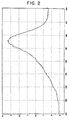
- a solution was prepared by dissolving 10 g of the hydrogenated polycyclic silicon compound obtained in Synthesis Example 1 in 10 ml of toluene. This solution was spin-coated on a substrate at 1,500 rpm in an argon atmosphere, and the solvent was removed at 100° C to form a coating film of the hydrogenated polycyclic silicon compound. Then, when this coating film was subjected to heat treatment at 500° C for 30 minutes in an argon atmosphere, it was converted into a silicon film having metal gloss. When the Raman spectrum of this silicon film was measured, it was 100% amorphous. The measured Raman spectrum is shown in Fig. 2.
- a coating solution prepared by dissolving 10 g of the hydrogenated polycyclic silicon compound obtained in Synthesis Example 1 in 30 ml of xylene was pattern-coated on a quartz substrate in an argon atmosphere. After this substrate was dried at 200° C in an argon atmosphere containing 5% of hydrogen, it was irradiated with an excimer laser having a wavelength of 308 nm to give a good silicon film pattern having a film thickness of 850 angstrom. When the Raman spectrum of this silicon film was measured, the silicon film was a polycrystalline silicon film having a crystallinity of 80%.
- a solution was prepared by dissolving 5 g of the hydrogenated polycyclic silicon compound obtained in Synthesis Example 2 in 10 g of toluene. This solution had a viscosity of 11 mPa ⁇ s.
- This solution was pattern-coated on a quartz substrate in an argon atmosphere by using an ink-jet head comprising a piezoelectric element. This substrate was dried at 150° C in an argon atmosphere and then thermally decomposed at 500° C to give a metal silicon film having a film thickness of 800 angstrom.
- this silicon film was subjected to surface composition analysis by ESCA, only silicon atoms were detected. Further, when the crystallinity of this silicon film by the Raman spectrum was measured, it was 100% amorphous.
- a solution was prepared in the same manner as in Example 1 except that tetrahydronaphthalene was used in place of toluene used as the solvent in Example 1.
- This solution ink was pattern-coated on a quartz substrate in an argon atmosphere by using an ink-jet head comprising a piezoelectric element.
- This substrate was dried at 150° C in an argon atmosphere containing 5% of hydrogen, then thermally decomposed at 500° C, and irradiated with ultraviolet light from a 500-W high-pressure mercury lamp for 10 minutes to give a metal silicon film having a film thickness of 650 angstrom.
- ESCA surface composition analysis by ESCA, only silicon atoms were detected. Further, when the crystallinity of this silicon film by the Raman spectrum was measured, it was 100% amorphous.
- the pattern coating was conducted on a polyimide film substrate in the same manner as in Example 1 except that a solution obtained by dissolving 5 g of the hydrogenated polycyclic silicon compound obtained in Synthesis Example 2 in a mixed solvent of 7 g of toluene and 3 g of diethylene glycol diethyl ether was used to spin coated on the substrate which was a polyimide film substrate.
- This substrate was dried at 150° C in an argon atmosphere and then optically and thermally decomposed at 350° C while exposed to a 500-W high-pressure mercury lamp to give a metal silicon film having a film thickness of 800 angstrom.
- this silicon film was subjected to surface composition analysis by ESCA, only silicon atoms were detected. Further, when the crystallinity of this silicon film by the Raman spectrum was measured, it was 100% amorphous.
- the 100%-amorphous silicon film obtained in Example 5 was irradiated with an excimer laser having a wavelength of 308 nm in an argon atmosphere. When the Raman spectrum was measured again, it was a polycrystalline silicon film having a crystallinity of 65%.
- This precipitate was separated by filtration, washed fully with water and then with cyclohexane, and vacuum dried to give 50 g of a phenyl group-containing boron-modified silicon compound.
- Fifty grams of the boron-modified silicon compound was dissolved in 500 ml of toluene, 2 g of aluminum chloride was added thereto, and a dried hydrogen chloride gas was then introduced thereto until the material disappeared. After the completion of the reaction, the aluminum compound was removed therefrom. Thereafter, the solvent was separated by distillation under reduced pressure to give 25 g of the chlorinated compound.
- This precipitate was separated by filtration, washed fully with water and dried to give 90 g of a phenyl group-containing boron-modified silane compound.
- Ninety grams of the modified silane compound was dissolved in 500 ml of toluene, 4 g of aluminum chloride was added thereto, and a dried hydrogen chloride gas was then introduced to the resulting mixture, while the mixture was cooled with ice, until the material disappeared. After the completion of the reaction, the aluminum compound was removed therefrom. Thereafter, the modified silane compound was converted into a chloro group-containing boron-modified silane compound.
- This chlorinated compound without purifying it, was dissolved in a mixed solvent of 250 ml of ether and 250 ml of toluene in an argon atmosphere. Twelve grams of lithium aluminum hydride was added to the resulting mixture while the mixture was agitated and cooled with ice, and the mixture was agitated for another 3 hours. After the aluminum compound was separated from the reaction mixture, the remaining mixture was condensed and purified to give 10 g of the target modified silicon compound mixture. As a result of elementary analysis, it was found to be Si 5 H 11 B.
- a phosphorous-modified silicon compound mixture was obtained in the same manner as in Synthesis Example 1 except that 27 g of phosphorus tribromide was used in place of 25 g of boron tribromide used in the above Synthesis Example 3. As a result of elementary analysis, it was found to be Si 5 H 5 P.
- a phosphorous-modified silicon compound mixture was obtained in the same manner as in Synthesis Example 3 except that 27 g of phosphorus tribromide was used in place of 25 g of boron tribromide used in the above Synthesis Example 4. As a result of elementary analysis, it was found to be Si 5 H 11 P.
- a coating solution was prepared by dissolving 3 g of the boron-modified silicon compound mixture obtained in Synthesis Example 3 in 10 ml of toluene. This solution had a viscosity of 6 mPa ⁇ s. This solution was spin-coated on a quartz substrate in an argon atmosphere, dried at 150° C and then thermally decomposed in an argon atmosphere at 500° C to give a metal silicon film having a film thickness of 650 angstrom. When this silicon film was subjected to surface composition analysis by ESCA, only silicon atoms and boron atoms were detected, and their ratio was 5:1. Further, when the crystallinity of this silicon film by the Reman spectrum was measured, it was 100% amorphous.
- a coating solution was prepared by dissolving 1 g of the boron-modified silicon compound mixture obtained in Synthesis Example 3 and 10 g of cyclohexasilane in 30 g of tetrahydronaphthalene. This solution had a viscosity of 10 mPa ⁇ s. This solution was dip-coated on a quartz substrate in an argon atmosphere and dried at 200° C to give a good film. When this substrate was heat-treated as in Example 7, the film was converted into a silicon film. When this silicon film was subjected to surface composition analysis by ESCA, only silicon atoms and boron atoms were detected, and their ratio was 50:1. Further, when the crystallinity of this silicon film by the Raman spectrum was measured, it was 100% amorphous.
- Example 8 When the 100% amorphous silicon film obtained by thermal decomposition in Example 8 was further heated to 800° C in an argon atmosphere, a sharp peak was observed at 520 cm -1 by the Raman spectrum. As a result of analysis, it was a polycrystalline silicon film having a crystallinity of 50%.
- a coating solution was prepared by dissolving 1 g of the phosphorous-modified silane compound mixture obtained in Synthesis Example 5 and 10 g of cyclohexasilane in 25 g of toluene. This solution had a viscosity of 8.5 mPa ⁇ s. This solution was spin-coated on a quartz substrate on which gold had been vapor-deposited in an argon atmosphere and dried at 150° C to give a good film. When this substrate was heat-treated as in Example 7, the film was converted into a silicon film. When this silicon film was subjected to surface composition analysis by ESCA, only silicon atoms and phosphorous atoms were detected, and their ratio was 50:1. Further, when the crystallinity of this silicon film by the Raman spectrum was measured, it was 100% amorphous.
- a coating solution was prepared by dissolving 1 g of the silane compound obtained in Synthesis Example 6 in a mixed solvent of 3 g of toluene, 3 g of xylene and 3 g of tetrahydronaphthalene. This solution had a viscosity of 11 mPa ⁇ s. This solution was spin-coated on a quartz substrate in an argon atmosphere, dried at 200° C, and irradiated with ultraviolet light from a 500-W high-pressure mercury lamp for 30 minutes while heated to 300° C in an argon atmosphere, to give a metal silicon film having a film thickness of 350 angstrom.
- a silicon film or a modified silicon film can be formed by a novel coating process different from conventional silicon film-forming processes.
- the material when the first coating composition is used, the material is not deposited from a vapor phase as in conventional CVD but the material in a liquid phase is coated and can be then converted into a silicon film as an electron material by thermal and/or optical energy.
- the second coating composition of the present invention unlike the deposition from a vapor phase as in conventional CVD or the ion injection in a vacuum, the material in a liquid phase is coated and can be then converted into a modified silicon film by thermal and/or optical energy.
- the modified silicon film pattern can be formed by partial coating without going through photolithography and etching processes. Therefore, semiconductor devices such as LSI, thin-film transistor, photoelectric converter and photosensitive which have the modified silicon film can be produced by an energy-efficient process.
Landscapes
- Chemical & Material Sciences (AREA)
- Engineering & Computer Science (AREA)
- Organic Chemistry (AREA)
- Life Sciences & Earth Sciences (AREA)
- Materials Engineering (AREA)
- Wood Science & Technology (AREA)
- Inorganic Chemistry (AREA)
- Physics & Mathematics (AREA)
- Plasma & Fusion (AREA)
- Paints Or Removers (AREA)
- Silicon Polymers (AREA)
- Electrodes Of Semiconductors (AREA)
- Silicon Compounds (AREA)
Applications Claiming Priority (5)
| Application Number | Priority Date | Filing Date | Title |
|---|---|---|---|
| JP8854299 | 1999-03-30 | ||
| JP8854299 | 1999-03-30 | ||
| JP8854199 | 1999-03-30 | ||
| JP8854199 | 1999-03-30 | ||
| PCT/JP2000/001960 WO2000058409A1 (fr) | 1999-03-30 | 2000-03-29 | Composition pour revetement |
Publications (2)
| Publication Number | Publication Date |
|---|---|
| EP1092755A1 true EP1092755A1 (fr) | 2001-04-18 |
| EP1092755A4 EP1092755A4 (fr) | 2004-12-22 |
Family
ID=26429908
Family Applications (1)
| Application Number | Title | Priority Date | Filing Date |
|---|---|---|---|
| EP00912922A Withdrawn EP1092755A4 (fr) | 1999-03-30 | 2000-03-29 | Composition pour revetement |
Country Status (7)
| Country | Link |
|---|---|
| US (1) | US6527847B1 (fr) |
| EP (1) | EP1092755A4 (fr) |
| JP (1) | JP4508428B2 (fr) |
| KR (1) | KR20010052441A (fr) |
| CN (1) | CN1250655C (fr) |
| TW (1) | TW539709B (fr) |
| WO (1) | WO2000058409A1 (fr) |
Cited By (1)
| Publication number | Priority date | Publication date | Assignee | Title |
|---|---|---|---|---|
| EP1284306A3 (fr) * | 2001-08-14 | 2004-05-19 | JSR Corporation | Composition de silanes, procédé de production d'un film en silicium et d' une cellule solaire |
Families Citing this family (28)
| Publication number | Priority date | Publication date | Assignee | Title |
|---|---|---|---|---|
| JP2003055556A (ja) * | 2001-08-14 | 2003-02-26 | Jsr Corp | シリコン膜またはシリコン酸化膜の形成方法およびそのための組成物 |
| JP2003313299A (ja) | 2002-04-22 | 2003-11-06 | Seiko Epson Corp | 高次シラン組成物及び該組成物を用いたシリコン膜の形成方法 |
| CN100423197C (zh) * | 2002-08-23 | 2008-10-01 | Jsr株式会社 | 硅膜形成用组合物和硅膜的形成方法 |
| US7879696B2 (en) * | 2003-07-08 | 2011-02-01 | Kovio, Inc. | Compositions and methods for forming a semiconducting and/or silicon-containing film, and structures formed therefrom |
| JP4636236B2 (ja) * | 2003-10-16 | 2011-02-23 | Jsr株式会社 | シリコン・コバルト膜形成用組成物およびシリコン・コバルト膜の形成方法 |
| US7498015B1 (en) | 2004-02-27 | 2009-03-03 | Kovio, Inc. | Method of making silane compositions |
| US8211396B1 (en) | 2004-09-24 | 2012-07-03 | Kovio, Inc. | Heterocyclic semiconductor precursor compounds, compositions containing the same, and methods of making such compounds and compositions |
| US7314513B1 (en) * | 2004-09-24 | 2008-01-01 | Kovio, Inc. | Methods of forming a doped semiconductor thin film, doped semiconductor thin film structures, doped silane compositions, and methods of making such compositions |
| US7674926B1 (en) | 2004-10-01 | 2010-03-09 | Kovio, Inc. | Dopant group-substituted semiconductor precursor compounds, compositions containing the same, and methods of making such compounds and compositions |
| US7485691B1 (en) * | 2004-10-08 | 2009-02-03 | Kovio, Inc | Polysilane compositions, methods for their synthesis and films formed therefrom |
| EP1943669A4 (fr) * | 2005-10-05 | 2012-06-13 | Kovio Inc | Polysilanes, polygermanes de poids moléculaire élevé linéaires et réticulés et copolymères de ceux-ci, compositions contenant ceux-ci, et procédés de fabrication et d'utilisation de tels composés et compositions |
| US7709307B2 (en) * | 2006-08-24 | 2010-05-04 | Kovio, Inc. | Printed non-volatile memory |
| DE102006043929B4 (de) * | 2006-09-14 | 2016-10-06 | Spawnt Private S.À.R.L. | Verfahren zur Herstellung von festen Polysilanmischungen |
| WO2008045327A2 (fr) * | 2006-10-06 | 2008-04-17 | Kovio, Inc. | Polymères de silicium, procédés pour polymériser des composés de silicium, et procédés pour former des films minces de polymères de silicium |
| US20080138966A1 (en) * | 2006-11-15 | 2008-06-12 | Rogojina Elena V | Method of fabricating a densified nanoparticle thin film with a set of occluded pores |
| US20090053507A1 (en) * | 2007-08-17 | 2009-02-26 | Ndsu Research Foundation | Convergent-divergent-convergent nozzle focusing of aerosol particles for micron-scale direct writing |
| US8460983B1 (en) | 2008-01-21 | 2013-06-11 | Kovio, Inc. | Method for modifying and controlling the threshold voltage of thin film transistors |
| JP2008143782A (ja) * | 2008-02-08 | 2008-06-26 | Jsr Corp | 太陽電池の製造方法 |
| WO2009148878A2 (fr) * | 2008-05-29 | 2009-12-10 | Ndsu Research Foundation | Procédé de formation de silanes fonctionnalisés |
| US8624049B2 (en) * | 2010-01-18 | 2014-01-07 | Kovio, Inc. | Dopant group-substituted semiconductor precursor compounds, compositions containing the same, and methods of making such compounds and compositions |
| US8975429B2 (en) | 2010-01-28 | 2015-03-10 | Ndsu Research Foundation | Method of producing cyclohexasilane compounds |
| US8669169B2 (en) | 2010-09-01 | 2014-03-11 | Piquant Research Llc | Diffusion sources from liquid precursors |
| DE102010037278A1 (de) * | 2010-09-02 | 2012-03-08 | Hans Freitag | Verfahren zum Herstellen von Silizium-basierenden Schichten oder Silizium-basierenden Strukturen unter Verwendung von Silizium-enthaltenden Tinten |
| DE102010040231A1 (de) * | 2010-09-03 | 2012-03-08 | Evonik Degussa Gmbh | p-Dotierte Siliciumschichten |
| DE102012221669A1 (de) * | 2012-11-27 | 2014-05-28 | Evonik Industries Ag | Verfahren zum Herstellen kohlenstoffhaltiger Hydridosilane |
| WO2016205405A1 (fr) * | 2015-06-19 | 2016-12-22 | Ndsu Research Foundation | Polymère de coordination |
| US11117807B2 (en) * | 2017-06-23 | 2021-09-14 | Jiangsu Nata Opto-Electronic Materials Co. Ltd. | Method of making aluminum-free neopentasilane |
| US11649560B2 (en) * | 2019-06-20 | 2023-05-16 | Applied Materials, Inc. | Method for forming silicon-phosphorous materials |
Family Cites Families (16)
| Publication number | Priority date | Publication date | Assignee | Title |
|---|---|---|---|---|
| US3379512A (en) * | 1965-06-07 | 1968-04-23 | R I Patents Inc | Perfluoroborosilanes and methods of preparation |
| GB2077710B (en) | 1980-06-11 | 1983-10-12 | Nat Res Dev | Synthesising a polysilane |
| US4695331A (en) * | 1985-05-06 | 1987-09-22 | Chronar Corporation | Hetero-augmentation of semiconductor materials |
| EG18056A (en) | 1986-02-18 | 1991-11-30 | Solarex Corp | Dispositif feedstock materials useful in the fabrication of hydrogenated amorphous silicon alloys for photo-voltaic devices and other semiconductor devices |
| JPS6429661A (en) | 1987-07-24 | 1989-01-31 | Mikuni Kogyo Kk | Air-fuel mixture feeder |
| JPH02101463A (ja) * | 1988-10-11 | 1990-04-13 | Matsushita Electric Ind Co Ltd | 微細パターン形成材料およびパターン形成方法 |
| JP2730156B2 (ja) * | 1989-03-24 | 1998-03-25 | 日本電気株式会社 | 多結晶シリコン膜の形成方法 |
| JP2556131B2 (ja) * | 1989-04-06 | 1996-11-20 | 日本電気株式会社 | 層間絶縁膜の形成方法 |
| JPH04334551A (ja) | 1991-05-10 | 1992-11-20 | Tonen Corp | ヒドロシランの重合触媒 |
| JP3517934B2 (ja) | 1994-03-24 | 2004-04-12 | 昭和電工株式会社 | シリコン膜の形成方法 |
| JPH09237927A (ja) * | 1995-12-26 | 1997-09-09 | Toshiba Corp | 半導体薄膜形成方法および太陽電池の製造方法 |
| JP3408399B2 (ja) * | 1997-05-23 | 2003-05-19 | シャープ株式会社 | シリコン膜の形成方法 |
| JP2000007317A (ja) * | 1998-06-19 | 2000-01-11 | Sharp Corp | シリコン膜の形成方法 |
| WO2000059014A1 (fr) * | 1999-03-30 | 2000-10-05 | Seiko Epson Corporation | cROCEDE PRODUCTION D'UN FILM DE SILICIUM ET COMPOSITION D'ENCRE POUR IMPRIMANTE A JET D'ENCRE |
| CN1223011C (zh) * | 1999-03-30 | 2005-10-12 | 精工爱普生株式会社 | 太阳能电池的制造方法 |
| DE60039744D1 (de) * | 1999-03-30 | 2008-09-18 | Seiko Epson Corp | Verfahren zur Hersltellung einer Siliziumschicht |
-
2000
- 2000-03-29 TW TW089105859A patent/TW539709B/zh not_active IP Right Cessation
- 2000-03-29 KR KR1020007013457A patent/KR20010052441A/ko not_active Withdrawn
- 2000-03-29 EP EP00912922A patent/EP1092755A4/fr not_active Withdrawn
- 2000-03-29 WO PCT/JP2000/001960 patent/WO2000058409A1/fr not_active Ceased
- 2000-03-29 US US09/701,377 patent/US6527847B1/en not_active Expired - Lifetime
- 2000-03-29 CN CNB008004773A patent/CN1250655C/zh not_active Expired - Fee Related
- 2000-03-29 JP JP2000608695A patent/JP4508428B2/ja not_active Expired - Fee Related
Cited By (4)
| Publication number | Priority date | Publication date | Assignee | Title |
|---|---|---|---|---|
| EP1284306A3 (fr) * | 2001-08-14 | 2004-05-19 | JSR Corporation | Composition de silanes, procédé de production d'un film en silicium et d' une cellule solaire |
| US7067069B2 (en) | 2001-08-14 | 2006-06-27 | Jsr Corporation | Silane composition, silicon film forming method and solar cell production method |
| US7173180B2 (en) | 2001-08-14 | 2007-02-06 | Jsr Corporation | Silane composition, silicon film forming method and solar cell production method |
| CN100392008C (zh) * | 2001-08-14 | 2008-06-04 | Jsr株式会社 | 硅烷组合物、硅膜的形成方法和太阳能电池的制造方法 |
Also Published As
| Publication number | Publication date |
|---|---|
| KR20010052441A (ko) | 2001-06-25 |
| CN1250655C (zh) | 2006-04-12 |
| CN1297471A (zh) | 2001-05-30 |
| EP1092755A4 (fr) | 2004-12-22 |
| TW539709B (en) | 2003-07-01 |
| JP4508428B2 (ja) | 2010-07-21 |
| US6527847B1 (en) | 2003-03-04 |
| WO2000058409A1 (fr) | 2000-10-05 |
Similar Documents
| Publication | Publication Date | Title |
|---|---|---|
| US6527847B1 (en) | Coating composition | |
| KR100436319B1 (ko) | 실리콘 막의 형성방법 | |
| EP1284306B1 (fr) | Composition de silanes, procédé de production d'un film en silicium et d' une cellule solaire | |
| US6517911B1 (en) | Process for the formation of silicon oxide films | |
| US6503570B2 (en) | Cyclosilane compound, and solution composition and process for forming a silicon film | |
| EP1087428B1 (fr) | Procédé de formation d'un film de silicium et composition d'encre pour imprimante à jet d'encre | |
| JPWO2000058409A1 (ja) | コーティング組成物 | |
| JPWO2000059015A1 (ja) | シリコン膜の形成方法 | |
| JP2003171556A (ja) | シリコン膜の形成方法およびそのための組成物 | |
| JP4462394B2 (ja) | シリコン膜のパターン形成方法 | |
| JP4419357B2 (ja) | シラン組成物及びそれを用いた太陽電池の製造方法 | |
| JP4748288B2 (ja) | スピロ[4.4]ノナシランを含有する組成物 | |
| JP2005223138A (ja) | シリコン膜の成膜方法及び当該シリコン膜の成膜方法を使用するデバイスの製造方法 | |
| JP2001058996A (ja) | ノルボルニル基を持つシリコン化合物、コーティング組成物およびシリコン膜の製造法 | |
| JPWO2000059022A1 (ja) | シリコン酸化膜の形成方法 | |
| JP2008143782A (ja) | 太陽電池の製造方法 |
Legal Events
| Date | Code | Title | Description |
|---|---|---|---|
| PUAI | Public reference made under article 153(3) epc to a published international application that has entered the european phase |
Free format text: ORIGINAL CODE: 0009012 |
|
| 17P | Request for examination filed |
Effective date: 20010118 |
|
| AK | Designated contracting states |
Kind code of ref document: A1 Designated state(s): AT BE CH CY DE DK ES FI FR GB GR IE IT LI LU MC NL PT SE |
|
| RIC1 | Information provided on ipc code assigned before grant |
Free format text: 7C 09D 1/00 A, 7C 09D 183/16 B, 7C 08G 77/60 B, 7C 01B 33/04 B, 7H 01L 21/205 J, 7H 01L 21:28 J, 7H 01L 21:288 J |
|
| RAP1 | Party data changed (applicant data changed or rights of an application transferred) |
Owner name: JSR CORPORATION |
|
| RBV | Designated contracting states (corrected) |
Designated state(s): DE FR GB NL |
|
| STAA | Information on the status of an ep patent application or granted ep patent |
Free format text: STATUS: THE APPLICATION HAS BEEN WITHDRAWN |
|
| A4 | Supplementary search report drawn up and despatched |
Effective date: 20041105 |
|
| RIC1 | Information provided on ipc code assigned before grant |
Ipc: 7C 08G 77/60 B Ipc: 7C 01B 33/04 B Ipc: 7C 01B 33/08 B Ipc: 7C 23C 18/12 B Ipc: 7C 09D 1/00 A Ipc: 7C 09D 183/16 B |
|
| 18W | Application withdrawn |
Effective date: 20041208 |