EP1093143A1 - Flip-chip montiertes Mikrorelais auf einer integrierten Schaltung - Google Patents
Flip-chip montiertes Mikrorelais auf einer integrierten Schaltung Download PDFInfo
- Publication number
- EP1093143A1 EP1093143A1 EP00308858A EP00308858A EP1093143A1 EP 1093143 A1 EP1093143 A1 EP 1093143A1 EP 00308858 A EP00308858 A EP 00308858A EP 00308858 A EP00308858 A EP 00308858A EP 1093143 A1 EP1093143 A1 EP 1093143A1
- Authority
- EP
- European Patent Office
- Prior art keywords
- chip
- mems
- integrated circuit
- relay
- hybrid
- Prior art date
- Legal status (The legal status is an assumption and is not a legal conclusion. Google has not performed a legal analysis and makes no representation as to the accuracy of the status listed.)
- Withdrawn
Links
Images


Classifications
-
- B—PERFORMING OPERATIONS; TRANSPORTING
- B81—MICROSTRUCTURAL TECHNOLOGY
- B81C—PROCESSES OR APPARATUS SPECIALLY ADAPTED FOR THE MANUFACTURE OR TREATMENT OF MICROSTRUCTURAL DEVICES OR SYSTEMS
- B81C1/00—Manufacture or treatment of devices or systems in or on a substrate
- B81C1/00015—Manufacture or treatment of devices or systems in or on a substrate for manufacturing microsystems
- B81C1/00222—Integrating an electronic processing unit with a micromechanical structure
- B81C1/00238—Joining a substrate with an electronic processing unit and a substrate with a micromechanical structure
-
- H—ELECTRICITY
- H01—ELECTRIC ELEMENTS
- H01H—ELECTRIC SWITCHES; RELAYS; SELECTORS; EMERGENCY PROTECTIVE DEVICES
- H01H50/00—Details of electromagnetic relays
- H01H50/005—Details of electromagnetic relays using micromechanics
-
- H—ELECTRICITY
- H01—ELECTRIC ELEMENTS
- H01H—ELECTRIC SWITCHES; RELAYS; SELECTORS; EMERGENCY PROTECTIVE DEVICES
- H01H59/00—Electrostatic relays; Electro-adhesion relays
- H01H59/0009—Electrostatic relays; Electro-adhesion relays making use of micromechanics
-
- B—PERFORMING OPERATIONS; TRANSPORTING
- B81—MICROSTRUCTURAL TECHNOLOGY
- B81B—MICROSTRUCTURAL DEVICES OR SYSTEMS, e.g. MICROMECHANICAL DEVICES
- B81B2203/00—Basic microelectromechanical structures
- B81B2203/01—Suspended structures, i.e. structures allowing a movement
- B81B2203/0118—Cantilevers
-
- B—PERFORMING OPERATIONS; TRANSPORTING
- B81—MICROSTRUCTURAL TECHNOLOGY
- B81B—MICROSTRUCTURAL DEVICES OR SYSTEMS, e.g. MICROMECHANICAL DEVICES
- B81B2203/00—Basic microelectromechanical structures
- B81B2203/04—Electrodes
Definitions
- the present invention relates to hybrid integrated circuits having micro-electromechanical systems (MEMS) chips bonded to CMOS chips. More specifically, the present invention relates to MEMS relays integrated on CMOS circuitry.
- MEMS micro-electromechanical systems
- Mechanical relays play an important role in various electronic systems. Examples of such systems include communication switch equipment for individual phone connections and electronic test equipment wherein functions like "range selection" may be implemented using mechanical relays. Solid state switches that replace mechanical relays and provide electrical connection and isolation using semiconductor materials are widely used in many applications. However, such solid state switches possess relatively low off-state resistance and have limited bandwidth. For applications where such properties are necessary, mechanical relays are therefore still widely used.
- the mechanical relay is the single component that occupies the most space in the total system core hardware.
- the mechanical relay is the single component that occupies the most space in the total system core hardware.
- the mechanical relay is the single component that occupies the most space in the total system core hardware.
- the integration scale of CMOS circuitry increases, the number of mechanical relays that need to be connected to such a CMOS chip increases. Since the physical space around the CMOS chip is limited, larger-scale integration of additional physical components becomes more difficult, eventually reaching a point of diminishing returns wherein it is simply not possible to add additional parts, such as additional mechanical relays, to the circuit.
- connection between the CMOS chip and the mechanical relays must be designed to accommodate the required bandwidth.
- the connection is carefully designed the physical distance between the relay and the chip introduces a time delay in communication between them.
- conventional mechanical relays that are widely used today are bulky and expensive, so that utilizing them in densely packed integrated circuit designs is prohibitive.
- relays that can be used with integrated circuits and that are cost-effective and easily integrable.
- Such relays should be integrable with the circuitry architecture of the chip and be adaptable for wide bandwidth applications.
- the present invention provides an article comprising a MEMS chip which includes a micromachined mechanical relay fabricated in a MEMS fabrication process.
- This MEMS chip is bonded to an integrated circuit where relay action is required, that is, there are connections on this IC chip that need to be established when necessary. Actuation of MEMS relays on the MEMS chip will establish connections in the integrated circuit chips via mechanical action.
- the MEMS chip is flip-chip bonded to the integrated circuit chip, although other bonding techniques may be employed.
- the inventive hybrid circuits provide the functionality of a relay on and integrated with an integrated circuit. While it is preferred that the integrated circuit chip be a CMOS integrated circuit chip, any type of integrated circuit chip that can be bonded to a MEMS chip having a micromachined relay in accordance with the invention may utilize the inventive techniques disclosed and claimed herein. As the integration level of the integrated circuits increases, the number of relays that need to be integrated also increases. The conventional methods, where in separate mechanical relays are individually bonded to an integrated circuit, have severe limitations in this respect, since the edge to which relays can be bonded to is limited. Going to a larger number of relays in conventional technology requires a fan-out structure of the electrical interconnects, and thus a time delay in the communication between the integrated circuits and the relays.
- Such integration bottleneck is absent in the bonded hybrid chip disclosed in the present invention. Moreover, by using a careful embodiment of the inventive MEMS relays, valuable integrated circuit real estate can be conserved, thereby increasing the efficiency of fabricating hybrid integrated circuits. Additionally, by bonding the integrated circuits to the MEMS chips electrical communication delays between the relays on the MEMS chip and the circuitry on the integrated circuit chip are greatly reduced which allows the hybrid circuits of the present invention to be used in high bandwidth applications.
- Circuit 10 may for example comprise a conventional integrated circuit chip 20 that contains the circuit elements to perform the particular functions for which the hybrid circuit 10 is designed.
- integrated circuit 20 is a CMOS circuit, but those skilled in the art will appreciate that any type of integrated circuit may be used in hybrid circuit 10.
- CMOS integrated circuit chip 20 further comprises a substrate 30 which conventionally comprises silicon, but may also comprise other semiconductor materials such as Ge, GaAs, InP and others depending on the particular application intended for the hybrid circuits of the present invention.
- the MEMS chip 40 comprises a micro-relay that is agreeable as an electrostatically actuated switch.
- the micro-relay includes a mobile micromachine 50 that carries an electrical contact pad or bridge electrode 60 movable with the micromachine 50 into electrical contact with an element on CMOS chip 20 to complete the electrical connection between the two chips.
- the mobile micromachine 50 comprises a cantilever arm 70 having an end 80 anchored to a substrate 90 of MEMS chip 40.
- Substrate 90 also conventionally comprises silicon, but ultimately similarly comprise other semiconductor materials depending on the particular applications in which the MEMS devices fabricated thereon will be used.
- the bridge electrode 60 has a thickness of from about 0.01 microns to about 10 microns on its top. Still more preferably, the cantilever arm 70 has a width from about 1 micron to about 10,000 microns on each side and a thickness from about 0.01 microns to about 10 microns.
- the cantilever arm 70 may comprise an insulator-like silicon dioxide or silicon nitride composition.
- the cantilever arm 70 may comprise a conductor and the electrical bridge contact or pad 60 may be deposited above an insulating layer (not shown in the Figures) on cantilever arm 70.
- the thickness of the insulating layer will be between about 0.01 microns and about 100 microns.
- the CMOS chip 20 further comprises the requisite contact electrodes 100 that will allow the cantilever arm 70 and electrode 60 to complete the electrical connection necessary for the circuit function.
- Both the MEMS chip 40 and the CMOS chip 30 also comprise actuation electrodes 95 fabricated on their respective substrates 90, 30 and to operatively pull the mobile micromachine cantilever arm 70 and bridge electrode 60 towards the contact electrodes 100 with an electrostatic force created by selectively applying a voltage to the electrodes 95. In this manner, electrical contact can be made between contact electrodes 100 and the bridge electrode 60 so that a robust electrical connection can be effectuated between the contact electrodes 100 to ensure that stable transmission of electrical signals can take place through the contact electrodes 100.
- the CMOS chip 20 is fabricated using conventional CMOS fabrication technology, while the MEMS chip 40 is fabricated using a MEMS fabrication process. Alternately, commercial MEMS micro-relays may be used such as those available from Cronos Integrated Microsystems, Inc., of Research Triangle Park, North Carolina.
- the two chips are bonded using a heat activation technique wherein a heat sensitive adhesive is applied between the two parts to be bonded together, following which heat and pressure applied to the two pieces so that the adhesive can anneal. Upon cooling, a hard, solid seal between the two substrates treated with the adhesive has been created.
- a spacing or gap 110 between the chips 20, 40 will be formed. That gap and more particularly the spacing between each of the actuation electrodes 95 and the movable portion of the micromachine 50 -- is determinative of the correct or appropriate operating voltage for actuating the MEMS relay 50.
- the width of gap 110 is between about 0.1 microns and about 100 microns.
- the gap 110 can be controlled precisely during the flip-chip bonding process by utilizing spacers 120 (shown in Figure 3) of known thickness. Such spacers can be fabricated on either of the substrates 30, 90 using either the MEMS or the CMOS fabrication process, or both.
- the cantilever arm 70 When a voltage is applied between the actuation electrodes 95 and the mobile micromachine 50, the cantilever arm 70 is and moved or attracted towards the CMOS chip 20. In this manner, the bridge electrode 60 the mobile micromachine 50 establishes the electrical connection to the contact electrodes 100 on the CMOS chip 20.
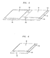
- FIG. 4 depicts a preferred embodiment of a hybrid circuit of the invention wherein illustrating the integration.
- the electrical interconnection between the CMOS chip 20 and MEMS chip 40 may be laid out during the CMOS fabrication process, in which, a separate CMOS-MEMS interconnection pad 130 is joined from the CMOS chip 20 to the MEMS chip 40, to establish an electrical connection therebetween.
- MEMS relays 50 are preferably integrated onto part of the CMOS chip 20 by flip-chip bonding, as described above.
- the contact electrodes 100 and the actuation electrode 95 necessary for completing the relay function are fabricated on CMOS chip at the area underneath where the MEMS chip is flip-chip bonded.
- This embodiment is relatively simple to implement, but suffers from the fact that the CMOS-MEMS interconnection 130, the contact electrodes 100, and actuation electrodes 95 take up a large space and CMOS real estate can be quite expensive.
- a significant portion of the silicon chip that goes through CMOS processing actually does not carry CMOS circuitry but is rather dedicated to the interconnection 130 and mating electrodes 100, 95 for the MEMS relays, thus incurring unnecessary costs in fabrication of the CMOS chip.
- FIG. 5 A second approach to integrating the relay function is shown in Figure 5.
- a third carrier wafer 140 is fabricated, that carries the CMOS-MEMS electrical interconnect 130, the electrical connection pads 100, actuation electrodes 95, and the mating electrodes for CMOS chip.
- the CMOS chip 20 and MEMS chip 40 are then independently flip-chip bonded onto carrier wafer 140. Since wafer 140 does not itself proceed through the full CMOS fabrication process, the cost to produce the hybrid circuit of Figure 5 is very low.
- FIG. 6 Yet a third approach to the MEMS relay integration issue of the invention is shown in Figure 6.
- processing steps are added in the CMOS process to fabricate the MEMS relay electrical connections 100 and the actuation electrode 95 in the uppermost layers 150 of CMOS chip 20.
- the MEMS relay chip 40 is then directly flip-chip bonded onto CMOS chip 20, as discussed above. Because this embodiment requires a modification of the CMOS process itself, it should be considered only if the relay functionality is absolutely critical in the total performance of the CMOS chip.
- the inventive hybrid integrated circuits effectively integrate a MEMS relay with an integrated circuit chip cost-effectively and robustly.
- the inventive circuits utilize only a small amount of CMOS real estate and are particularly useful in high bandwidth applications. Such results have not heretofore been achieved in the art.
Landscapes
- Engineering & Computer Science (AREA)
- Manufacturing & Machinery (AREA)
- Physics & Mathematics (AREA)
- Electromagnetism (AREA)
- Microelectronics & Electronic Packaging (AREA)
- Micromachines (AREA)
Applications Claiming Priority (2)
| Application Number | Priority Date | Filing Date | Title |
|---|---|---|---|
| US41885799A | 1999-10-15 | 1999-10-15 | |
| US418857 | 1999-10-15 |
Publications (1)
| Publication Number | Publication Date |
|---|---|
| EP1093143A1 true EP1093143A1 (de) | 2001-04-18 |
Family
ID=23659828
Family Applications (1)
| Application Number | Title | Priority Date | Filing Date |
|---|---|---|---|
| EP00308858A Withdrawn EP1093143A1 (de) | 1999-10-15 | 2000-10-09 | Flip-chip montiertes Mikrorelais auf einer integrierten Schaltung |
Country Status (2)
| Country | Link |
|---|---|
| EP (1) | EP1093143A1 (de) |
| JP (1) | JP2001198897A (de) |
Cited By (11)
| Publication number | Priority date | Publication date | Assignee | Title |
|---|---|---|---|---|
| WO2004000719A1 (ja) * | 2002-06-21 | 2003-12-31 | Tokyo Electron Limited | Memsアレイとその製造方法及びそれに基づくmemsデバイスの製造方法 |
| WO2004046019A1 (es) * | 2002-11-19 | 2004-06-03 | Baolab Microsystems S.L. | Relé miniaturizado y sus usos correspondientes |
| US6861277B1 (en) | 2003-10-02 | 2005-03-01 | Hewlett-Packard Development Company, L.P. | Method of forming MEMS device |
| US6914709B2 (en) | 2003-10-02 | 2005-07-05 | Hewlett-Packard Development Company, L.P. | MEMS device and method of forming MEMS device |
| US6917459B2 (en) | 2003-06-03 | 2005-07-12 | Hewlett-Packard Development Company, L.P. | MEMS device and method of forming MEMS device |
| US6946321B1 (en) | 2001-12-05 | 2005-09-20 | National Semiconductor Corporation | Method of forming the integrated circuit having a die with high Q inductors and capacitors attached to a die with a circuit as a flip chip |
| ES2246693A1 (es) * | 2003-11-18 | 2006-02-16 | Baolab Microsystems S.L. | Circuito integrado con matriz de conexion analogica. |
| KR100732778B1 (ko) * | 2002-06-21 | 2007-06-27 | 동경 엘렉트론 주식회사 | Mems 어레이 및 그 제조 방법과, 그것에 기초한mems 디바이스의 제조 방법 |
| US7782026B2 (en) | 2004-05-19 | 2010-08-24 | Baolab Microsystems S.L. | Regulator circuit and corresponding uses |
| US7859370B2 (en) | 2004-03-31 | 2010-12-28 | Sharp Kabushiki Kaisha | Electrostatic actuator |
| CN104916501A (zh) * | 2015-04-30 | 2015-09-16 | 中国电子科技集团公司第四十一研究所 | 一种小型双重单刀双掷同轴机电开关 |
Families Citing this family (3)
| Publication number | Priority date | Publication date | Assignee | Title |
|---|---|---|---|---|
| US6743653B2 (en) | 2002-05-08 | 2004-06-01 | Nippon Telegraph And Telephone Corporation | Micromachine manufacturing method |
| US20030227035A1 (en) | 2002-06-05 | 2003-12-11 | Hiromu Ishii | Micromachine and manufacturing method therefor |
| US7208809B2 (en) | 2002-09-19 | 2007-04-24 | Nippon Telegraph And Telephone Corporation | Semiconductor device having MEMS |
Citations (5)
| Publication number | Priority date | Publication date | Assignee | Title |
|---|---|---|---|---|
| US4528583A (en) * | 1980-05-08 | 1985-07-09 | U.S. Philips Corporation | Programmable semiconductor device and method of manufacturing same |
| US5070317A (en) * | 1989-01-17 | 1991-12-03 | Bhagat Jayant K | Miniature inductor for integrated circuits and devices |
| US5578976A (en) * | 1995-06-22 | 1996-11-26 | Rockwell International Corporation | Micro electromechanical RF switch |
| WO1998006118A1 (en) * | 1996-08-05 | 1998-02-12 | Mcnc | Encapsulated micro-relay modules and methods of fabricating same |
| US5963793A (en) * | 1996-05-29 | 1999-10-05 | Mcnc | Microelectronic packaging using arched solder columns |
-
2000
- 2000-10-09 EP EP00308858A patent/EP1093143A1/de not_active Withdrawn
- 2000-10-16 JP JP2000314632A patent/JP2001198897A/ja active Pending
Patent Citations (5)
| Publication number | Priority date | Publication date | Assignee | Title |
|---|---|---|---|---|
| US4528583A (en) * | 1980-05-08 | 1985-07-09 | U.S. Philips Corporation | Programmable semiconductor device and method of manufacturing same |
| US5070317A (en) * | 1989-01-17 | 1991-12-03 | Bhagat Jayant K | Miniature inductor for integrated circuits and devices |
| US5578976A (en) * | 1995-06-22 | 1996-11-26 | Rockwell International Corporation | Micro electromechanical RF switch |
| US5963793A (en) * | 1996-05-29 | 1999-10-05 | Mcnc | Microelectronic packaging using arched solder columns |
| WO1998006118A1 (en) * | 1996-08-05 | 1998-02-12 | Mcnc | Encapsulated micro-relay modules and methods of fabricating same |
Cited By (19)
| Publication number | Priority date | Publication date | Assignee | Title |
|---|---|---|---|---|
| US6946321B1 (en) | 2001-12-05 | 2005-09-20 | National Semiconductor Corporation | Method of forming the integrated circuit having a die with high Q inductors and capacitors attached to a die with a circuit as a flip chip |
| CN1308221C (zh) * | 2002-06-21 | 2007-04-04 | 东京毅力科创株式会社 | Mems阵列、其制造方法以及mems器件制造方法 |
| WO2004000719A1 (ja) * | 2002-06-21 | 2003-12-31 | Tokyo Electron Limited | Memsアレイとその製造方法及びそれに基づくmemsデバイスの製造方法 |
| KR100732778B1 (ko) * | 2002-06-21 | 2007-06-27 | 동경 엘렉트론 주식회사 | Mems 어레이 및 그 제조 방법과, 그것에 기초한mems 디바이스의 제조 방법 |
| WO2004046019A1 (es) * | 2002-11-19 | 2004-06-03 | Baolab Microsystems S.L. | Relé miniaturizado y sus usos correspondientes |
| US7876182B2 (en) | 2002-11-19 | 2011-01-25 | Baolab Microsystems S. L. | Miniaturized relay and corresponding uses |
| US7446300B2 (en) | 2002-11-19 | 2008-11-04 | Baolab Microsystems, S. L. | Miniature electro-optic device having a conductive element for modifying the state of passage of light between inlet/outlet points and corresponding uses thereof |
| CN100410165C (zh) * | 2002-11-19 | 2008-08-13 | 宝兰微系统公司 | 小型继电器和相应的用途 |
| RU2325722C2 (ru) * | 2002-11-19 | 2008-05-27 | Баолаб Микросистемс С.Л. | Миниатюрное реле и соответствующие варианты его использования |
| US6917459B2 (en) | 2003-06-03 | 2005-07-12 | Hewlett-Packard Development Company, L.P. | MEMS device and method of forming MEMS device |
| US7310175B2 (en) | 2003-10-02 | 2007-12-18 | Hewlett-Packard Development Company, L.P. | MEMS device and method of forming MEMS device |
| US7079301B2 (en) | 2003-10-02 | 2006-07-18 | Hewlett-Packard Development Company, L.P. | MEMS device and method of forming MEMS device |
| US6914709B2 (en) | 2003-10-02 | 2005-07-05 | Hewlett-Packard Development Company, L.P. | MEMS device and method of forming MEMS device |
| US6861277B1 (en) | 2003-10-02 | 2005-03-01 | Hewlett-Packard Development Company, L.P. | Method of forming MEMS device |
| ES2246693B1 (es) * | 2003-11-18 | 2006-11-01 | Baolab Microsystems S.L. | Circuito integrado con matriz de conexion analogica. |
| ES2246693A1 (es) * | 2003-11-18 | 2006-02-16 | Baolab Microsystems S.L. | Circuito integrado con matriz de conexion analogica. |
| US7859370B2 (en) | 2004-03-31 | 2010-12-28 | Sharp Kabushiki Kaisha | Electrostatic actuator |
| US7782026B2 (en) | 2004-05-19 | 2010-08-24 | Baolab Microsystems S.L. | Regulator circuit and corresponding uses |
| CN104916501A (zh) * | 2015-04-30 | 2015-09-16 | 中国电子科技集团公司第四十一研究所 | 一种小型双重单刀双掷同轴机电开关 |
Also Published As
| Publication number | Publication date |
|---|---|
| JP2001198897A (ja) | 2001-07-24 |
Similar Documents
| Publication | Publication Date | Title |
|---|---|---|
| JP3538109B2 (ja) | マイクロマシンスイッチ | |
| US10508022B2 (en) | MEMS device and process for RF and low resistance applications | |
| JP4418465B2 (ja) | マルチステブルマイクロ電子機械スイッチスイッチ及びその製造方法 | |
| US6841839B2 (en) | Microrelays and microrelay fabrication and operating methods | |
| JP4763133B2 (ja) | マイクロ機械構成部品を使用した診断用医用超音波システムとトランスデューサ | |
| US7551048B2 (en) | Micro-relay and method of fabricating the same | |
| US6939784B2 (en) | Wafer scale package and method of assembly | |
| US7312678B2 (en) | Micro-electromechanical relay | |
| US6506989B2 (en) | Micro power switch | |
| EP1959472A2 (de) | Wärmeleitende Überlagerungsstruktur für MEMS-Vorrichtungen und Verfahren zur Herstellung einer wärmeleitenden Überlagerungsstruktur für MEMS-Vorrichtungen | |
| EP1391906A2 (de) | Mikroelektromechanische elektrostatische RF Schalter | |
| KR20000029835A (ko) | 밀봉된마이크로-릴레이모듈및그모듈을제조하는방법 | |
| JP2001198897A (ja) | 混成集積回路 | |
| JP5176148B2 (ja) | スイッチング素子および通信機器 | |
| US7463125B2 (en) | Microrelays and microrelay fabrication and operating methods | |
| US20050269688A1 (en) | Microelectromechanical systems (MEMS) devices integrated in a hermetically sealed package | |
| CN115196580A (zh) | 具有罩接触部的mems开关 | |
| US6750078B2 (en) | MEMS switch having hexsil beam and method of integrating MEMS switch with a chip | |
| US6246305B1 (en) | Apparatus and method for operating a micromechanical switch | |
| FR2848021A1 (fr) | Micro-commutateur electrostatique pour composants a faible tension d'actionnement | |
| US9284183B2 (en) | Method for forming normally closed micromechanical device comprising a laterally movable element | |
| JP4932506B2 (ja) | マイクロスイッチング素子 | |
| US20020097118A1 (en) | Current actuated switch | |
| KR100493532B1 (ko) | 정전식 양방향 미세기전 액추에이터 | |
| KR100977917B1 (ko) | 마이크로-전자기계 시스템을 갖춘 마이크로스위치 |
Legal Events
| Date | Code | Title | Description |
|---|---|---|---|
| PUAI | Public reference made under article 153(3) epc to a published international application that has entered the european phase |
Free format text: ORIGINAL CODE: 0009012 |
|
| AK | Designated contracting states |
Kind code of ref document: A1 Designated state(s): DE FR GB |
|
| AX | Request for extension of the european patent |
Free format text: AL;LT;LV;MK;RO;SI |
|
| 17P | Request for examination filed |
Effective date: 20011004 |
|
| STAA | Information on the status of an ep patent application or granted ep patent |
Free format text: STATUS: THE APPLICATION HAS BEEN WITHDRAWN |
|
| AKX | Designation fees paid |
Free format text: DE FR GB |
|
| 18W | Application withdrawn |
Withdrawal date: 20011119 |