EP1093148A1 - Dispositif d'affichage à plasma - Google Patents
Dispositif d'affichage à plasma Download PDFInfo
- Publication number
- EP1093148A1 EP1093148A1 EP00402827A EP00402827A EP1093148A1 EP 1093148 A1 EP1093148 A1 EP 1093148A1 EP 00402827 A EP00402827 A EP 00402827A EP 00402827 A EP00402827 A EP 00402827A EP 1093148 A1 EP1093148 A1 EP 1093148A1
- Authority
- EP
- European Patent Office
- Prior art keywords
- electrodes
- display device
- branch electrode
- main wiring
- plasma display
- Prior art date
- Legal status (The legal status is an assumption and is not a legal conclusion. Google has not performed a legal analysis and makes no representation as to the accuracy of the status listed.)
- Withdrawn
Links
Images


Classifications
-
- H—ELECTRICITY
- H01—ELECTRIC ELEMENTS
- H01J—ELECTRIC DISCHARGE TUBES OR DISCHARGE LAMPS
- H01J11/00—Gas-filled discharge tubes with alternating current induction of the discharge, e.g. alternating current plasma display panels [AC-PDP]; Gas-filled discharge tubes without any main electrode inside the vessel; Gas-filled discharge tubes with at least one main electrode outside the vessel
- H01J11/20—Constructional details
- H01J11/22—Electrodes, e.g. special shape, material or configuration
- H01J11/24—Sustain electrodes or scan electrodes
-
- H—ELECTRICITY
- H01—ELECTRIC ELEMENTS
- H01J—ELECTRIC DISCHARGE TUBES OR DISCHARGE LAMPS
- H01J11/00—Gas-filled discharge tubes with alternating current induction of the discharge, e.g. alternating current plasma display panels [AC-PDP]; Gas-filled discharge tubes without any main electrode inside the vessel; Gas-filled discharge tubes with at least one main electrode outside the vessel
- H01J11/10—AC-PDPs with at least one main electrode being out of contact with the plasma
- H01J11/12—AC-PDPs with at least one main electrode being out of contact with the plasma with main electrodes provided on both sides of the discharge space
-
- H—ELECTRICITY
- H01—ELECTRIC ELEMENTS
- H01J—ELECTRIC DISCHARGE TUBES OR DISCHARGE LAMPS
- H01J11/00—Gas-filled discharge tubes with alternating current induction of the discharge, e.g. alternating current plasma display panels [AC-PDP]; Gas-filled discharge tubes without any main electrode inside the vessel; Gas-filled discharge tubes with at least one main electrode outside the vessel
- H01J11/20—Constructional details
- H01J11/22—Electrodes, e.g. special shape, material or configuration
- H01J11/32—Disposition of the electrodes
-
- H—ELECTRICITY
- H01—ELECTRIC ELEMENTS
- H01J—ELECTRIC DISCHARGE TUBES OR DISCHARGE LAMPS
- H01J11/00—Gas-filled discharge tubes with alternating current induction of the discharge, e.g. alternating current plasma display panels [AC-PDP]; Gas-filled discharge tubes without any main electrode inside the vessel; Gas-filled discharge tubes with at least one main electrode outside the vessel
- H01J11/20—Constructional details
- H01J11/34—Vessels, containers or parts thereof, e.g. substrates
- H01J11/42—Fluorescent layers
-
- H—ELECTRICITY
- H01—ELECTRIC ELEMENTS
- H01J—ELECTRIC DISCHARGE TUBES OR DISCHARGE LAMPS
- H01J2211/00—Plasma display panels with alternate current induction of the discharge, e.g. AC-PDPs
- H01J2211/20—Constructional details
- H01J2211/22—Electrodes
- H01J2211/24—Sustain electrodes or scan electrodes
- H01J2211/245—Shape, e.g. cross section or pattern
-
- H—ELECTRICITY
- H01—ELECTRIC ELEMENTS
- H01J—ELECTRIC DISCHARGE TUBES OR DISCHARGE LAMPS
- H01J2211/00—Plasma display panels with alternate current induction of the discharge, e.g. AC-PDPs
- H01J2211/20—Constructional details
- H01J2211/22—Electrodes
- H01J2211/32—Disposition of the electrodes
- H01J2211/323—Mutual disposition of electrodes
Definitions
- the present invention relates to an alternate-current driven plasma display device.
- the flat-type display devices include a liquid crystal display device (LCD), an electroluminescence display device (ELD) and a plasma display device (PDP).
- LCD liquid crystal display device
- ELD electroluminescence display device
- PDP plasma display device
- the plasma display device has advantages in that it is relatively easy to produce a large screen and attain a wider viewing angle, that it has excellent durability against environmental factors such as temperatures, magnetism, vibrations, etc., and that it has a long lifetime.
- the plasma display device is therefore expected to be applicable not only to a home-use wall-hung television set but also to a public large-sized information terminal.
- each discharge cell is driven according to a principle similar to that of a fluorescent lamp, and generally, the discharge cells are put together on the order of hundreds of thousands to constitute a display screen.
- the plasma display device is largely classified into a direct-current driven type (DC type) and an alternate-current driven type (AC type) according to methods of applying a voltage to the discharge cells, and each type has advantages and disadvantages.
- the AC type plasma display device is suitable for a higher fineness, since ribs which work to separate the discharge cells within a display screen can be formed in the form of stripes. Further, it has an advantage that electrodes are less worn out and have a long lifetime since surfaces of the electrodes are covered with a dielectric material.
- Fig. 6 shows a typical example of a conventional AC type plasma display device.
- This AC type plasma display device comes under a so-called tri-electrode type, and discharging takes place mainly between a pair of sustain electrodes 113.
- a front panel 10 and a rear panel 20 are bonded to each other in their circumferential portions. Light emission from a fluorescent layer 24 on the rear panel 20 is viewed through the front panel 10.
- the front panel 10 comprises a transparent first substrate 11, pairs of sustain electrodes 113 composed of a transparent electrically conductive material and formed on the first substrate 11 in the form of stripes, bus electrodes 112 composed of a material having a lower electric resistivity than the sustain electrodes and provided for decreasing the impedance of the sustain electrodes 113, a dielectric layer 14 formed on the bus electrodes 112, the sustain electrodes 113 and the first substrate 11, and a protective layer 15 formed on the dielectric layer 14.
- the rear panel 20 comprises a second substrate 21, address electrodes (also called data electrodes) 22 formed on the second substrate 21 in the form of stripes, a dielectric film 23 formed on the second substrate 21 and the address electrodes 22, insulating ribs 25 formed in regions which are on the dielectric film 23 and between the adjacent address electrodes 22, and fluorescent layers 24 formed so as to be on, and to extend from, the surface of the dielectric film 23 and so as to be on side walls of the ribs 25.
- the ribs 25 extend in parallel with the address electrodes 22.
- Each fluorescent layer 24 is constituted of a red fluorescent layer 24R, a green fluorescent layer 24G or a blue fluorescent layer 24B, and the fluorescent layers 24R, 24G and 24B of these colours are provided in a predetermined order. Fig.
- FIG. 6 is an exploded perspective view, and in an actual device, top portions of the ribs 25 of the rear panel 20 are in contact with the protective layer 15 of the front panel 10.
- a region where a pair of the sustain electrodes 113 and the address electrode 22 positioned between the adjacent ribs 25 overlap corresponds to one discharge cell.
- a rare gas is sealed in each space surrounded by the adjacent ribs 25, one fluorescent layer 24 and the protective layer 15.
- the extending direction of the sustain electrodes 113 and the extending direction of the address electrodes 22 make an angle of 90°, and a region where a pair of the sustain electrodes 113 and one set of the fluorescent layers 24R, 24G and 24B for emitting light of three primary colours overlap corresponds to one pixel.
- Glow discharge takes place between each of pairs of the sustain electrodes 113, and a plasma display device of this type is accordingly called "surface discharge type".
- the fluorescent layer excited by irradiation of vacuum ultraviolet light generated according to glow discharge in the rare gas emits light of a colour characteristic of kinds of fluorescent materials. Vacuum ultraviolet light having a wavelength depending upon the kind of the sealed rare gas is generated.
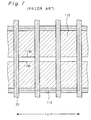
- Fig. 7 shows a schematic layout of the sustain electrodes 113, the bus electrodes 112 and the ribs 25 in the conventional plasma display device shown in Fig. 6.
- An area surrounded by dotted lines corresponds to one pixel.
- slanting lines are added.
- Each pixel has an almost square geometry.
- Each pixel is divided into three sections (cells) with the ribs 25, and each section emits light of one of three primary colours (R, G, B).
- R, G, B primary colours
- each pixel has an outer dimension Lo
- each section has dimensions slightly smaller than (L 0 /3) x (L 0 ).
- a portion 113A of each sustain electrode 113 which portion contributes to discharging has a length slightly smaller than (L 0 /3).
- Fig. 8 schematically shows a variant of layout of the sustain electrodes 113, the bus electrodes 112 and the ribs 25 in the conventional plasma display device.
- This variant is disclosed in JP-A-9-167565.
- This variant has a structure in which one sustain electrode 113 extends from one of a pair of the bus electrodes 112 toward the other of the pair of the bus electrodes 112.
- the plasma display device it is increasingly demanded to increase the density and fineness of pixels. For complying with such demands, it is inevitable to decrease the value of the outer dimension L 0 per pixel. As a result, the length [approximately (L 0 /3)] of those portions which contribute to discharging in a pair of the sustain electrodes 113 comes to be shorter, and the discharge regions decrease, which causes a problem that the brightness of the plasma display device decreases.
- the alternate-current driven type plasma display device of the present invention for achieving the above object has;
- first electrodes A plurality of the electrodes formed on the first substrate will be referred to as “first electrodes” for convenience, and the electrode group constituted of a plurality of the first electrodes will be referred to as “first electrode group”.
- the alternate-current type display device (to be referred to as "plasma display device” hereinafter) of the present invention has a structure in which the first panel and the second panel are arranged such that the dielectric layer is opposed to the fluorescent layers, that the extending direction of the main wirings and the extending direction of the ribs make a predetermined angle (for example, 90°), that a rare gas is sealed in each space surrounded by the dielectric layer, the fluorescent layer and a pair of the ribs, and that the fluorescent layer is irradiated with vacuum ultraviolet light generated by AC glow discharge which takes place between an opposed pair of the branch electrodes in the rare gas, to emit light.
- a region where one first electrode (combination of a pair of the first main wiring and the second main wiring and a pair of the first branch electrode and the second branch electrode) overlaps a pair of the ribs corresponds to one discharge cell.
- the first branch electrode extends in a direction counter to the direction in which the second branch electrode extends.
- the distance between the first branch electrode and the second branch electrode which are opposed to each other is preferably a predetermined distance, more preferably a constant distance.
- the first branch electrode and the second branch electrode may generally have a rectangular form when viewed as a plan view (that is, the first branch electrode and the second branch electrode may have a linear form), or they may have a zigzag form (i.e., a combination of dogleg forms, a combination of "S" letter forms or arc forms or a combination of any curved lines).
- the distance between the first branch electrode and the second branch electrode may be determined to have an arbitrary value, while the distance is 1 x 10 -4 m or less, preferably less than 5 x 10 -5 m, more preferably 4 x 10 -5 m or less, still more preferably 2.5 x 10 -5 m or less.
- the lower limit of the distance between the first branch electrode and the second branch electrode can be a distance at which no breakdown takes place between the first branch electrode and the second branch electrode.
- the pressure of the rare gas sealed in each space surrounded by the dielectric layer, the fluorescent layer and a pair of the ribs is from 1 x 10 2 Pa (0.001 atmospheric pressure) to 5 x 10 5 Pa (5 atmospheric pressures), preferably 1 x 10 3 Pa (0.01 atmospheric pressure) to 4 x 10 5 Pa (4 atmospheric pressures).
- the pressure of the rare gas in each space is adjusted to 1.0 x 10 2 Pa (0.001 atmospheric pressure) to 3.0 x 10 5 Pa (3 atmospheric pressures), preferably to 1.0 x 10 3 Pa (0.01 atmospheric pressure) to 2.0 x 10 5 Pa (2 atmospheric pressures), more preferably to 1.0 x 10 4 Pa (0.1 atmospheric pressure) to 1.0 x 10 5 Pa (1 atmospheric pressures).
- the fluorescent layers emit light when irradiated with vacuum ultraviolet light generated due to cathode glow in the rare gas.
- the sputtering ratio of various members constituting the plasma display device decreases with an increase in the pressure, and as a result, the plasma display device can have a longer lifetime.
- the comers of the top end portion of each first and second branch electrode are preferably removed or rounded.
- L 1 ⁇ L 2 is satisfied where L 1 is a distance between the first branch electrode and the second branch electrode and L 2 is a distance between the first main wiring and the top end portion of the second branch electrode or a distance between the second main wiring and the top end portion of the first branch electrode.
- a second electrode group constituted of a plurality of second electrodes may be formed on the first substrate, or may be formed on the second substrate.
- the second electrodes are formed on the dielectric layer through an insulating film, and the second electrodes make a predetermined angle (for example, 90°) from the extending direction of each main wiring.
- the second electrodes are formed on the second substrate, and the second electrodes make a predetermined angle (for example, 90°) from the extending direction of each main wiring, and the fluorescent layers are formed on or above the second electrodes.
- an electrically conductive material for the first and second main wirings and an electrically conductive material for the first and second branch electrodes are different from each other.
- the first and second main wirings have functions as bus electrodes in a conventional plasma display device.
- the first and second main wirings can be composed, typically, of a metal material such as Ag, Al, Ni, Cu and Cr, or a Cr/Cu/Cr stacked layer.
- the first and second main wirings composed of such a metal material or such a stacked layer is a factor which decreases a transmission quantity of visible light emitted from the fluorescent layers to pass through the first substrate and which therefore decreases the brightness of a display screen
- the first and second main wirings are preferably formed so as to be as narrow as possible so long as an electric resistance value necessary for the first electrodes can be obtained.
- the method of forming the first and second main wirings can be properly selected from a deposition method, a sputtering method, a screen printing method, a sandblasting method, a plating method and a lift-off method depending upon the electrically conductive material to be used.
- the electrically conductive material for the first and second branch electrodes differs depending upon whether the plasma display device is a transmission type or a reflection type.
- the transmission type plasma display device light emission from the fluorescent layers is observed through the second substrate, so that it does not cause any problem whether the electrically conductive material for the first and second branch electrodes is transparent or non-transparent.
- the second electrodes are desirably transparent.
- the reflection type plasma display device light emission from the fluorescent layers is observed through the first substrate. Therefore, when the second electrodes are formed on the second substrate, it does not cause any problem whether the electrically conductive material for the second electrodes is transparent or non-transparent, while the first and second branch electrodes are desirably transparent.
- the term "transparent or non-transparent” is based on the transmissivity of the electrically conductive material to light at a wavelength of emitted light (visible light region) inherent to the fluorescent materials. That is, when an electrically conductive material for the first and second branch electrodes is transparent to light emitted from the fluorescent layers, it can be said that the electrically conductive material is transparent.
- the non-transparent electrically conductive material includes Ni, Al, Au, Ag, Al, Pd/Ag, Cr, Ta, Cu, Ba, LaB 6 , Ca 0.2 La 0.8 CrO 3 , etc., and these materials may be used alone or in combination.
- the transparent electrically conductive material includes ITO (indium-tin oxide) and SnO 2 .
- the method of forming the first and second branch electrodes can be properly selected from a deposition method, a sputtering method, a screen printing method, a sandblasting method, a plating method and a lift-off method depending upon the electrically conductive material to be used. That is, an appropriate mask or a screen may be used to form the first and second branch electrodes having predetermined patterns, or after an electrically conductive material layer is formed on the entire surface, the electrically conductive material layer may be patterned to form the first and second branch electrodes.
- the dielectric layer since the dielectric layer is provided, the direct contact of ions and electrons to the first and second branch electrodes can be prevented. As a result, the wearing of the first and second branch electrodes can be prevented.
- the dielectric layer not only works to accumulate a wall charge, but also works as a resistor to suppress an excess discharge current and as a memory to sustain a discharge state.
- the material for the dielectric layer is required to be transparent, since light emission from the fluorescent layers is observed through the first substrate. For example, a low-melting glass is used as the above material.
- a protective layer is formed on the dielectric layer.
- the material for the protective layer can be selected from magnesium oxide (MgO), magnesium fluoride (MgF 2 ) and calcium fluoride (CaF 2 ).
- magnesium oxide is a suitable material having properties that it has a high secondary electron emission ratio and further that it shows a low sputtering ratio, a high transmissivity to light at a wavelength of light emitted from the fluorescent layers and a low discharge initiation voltage.
- the protective layer may have a stacked structure composed of at least two materials selected from the group consisting of the above materials.
- Examples of the material for the first substrate and the second substrate include a glass having a high strain point, soda glass (Na 2 O ⁇ CaO ⁇ SiO 2 ), borosilicate glass (Na 2 O ⁇ B 2 O 3 ⁇ SiO 2 ), forsterite (2MgO ⁇ SiO 2 ) and lead glass (Na 2 O ⁇ PbO ⁇ SiO 2 ).
- the material for the first substrate and the material for the second substrate may be the same as, or different from, each other.
- the plasma display device of the present invention is a so-called surface discharge type plasma display device. If the second electrodes are formed on the second substrate, and when the fluorescent layers have an insufficient function as a dielectric film, a dielectric film may be formed between the second electrode group and the fluorescent layers.
- the material for the dielectric film can be selected from a low-melting glass and SiO 2 .
- the fluorescent layers are composed of fluorescent materials selected from the group consisting of fluorescent materials which emit light of a red colour, fluorescent materials which emit light of a green colour and fluorescent materials which emit light of a blue colour, and the fluorescent layers are formed on or above the second substrate.
- the fluorescent layer composed of a fluorescence material which emits light for example, of a red colour (red fluorescent layer) is formed on or above one second electrode
- the fluorescent layer composed of a fluorescence material which emits light, for example, of a green colour (green fluorescent layer) is formed on or above another second electrode
- the fluorescent layer composed of a fluorescence material which emits light, for example, of a blue colour (blue fluorescent layer) is formed on or above still another second electrode.
- These three fluorescent layers for emitting light of three primary colours form one set, and such sets are provided in a predetermined order.
- the red fluorescent layer, the green fluorescent layer and the blue fluorescent layer are formed on the second substrate, these three fluorescent layers form one set, and such sets are provided in a predetermined order.
- a region where one first electrode (a combination of a pair of the first and second main wirings and a pair of the first and second branch electrodes) and one set of the fluorescent layers which emit light of three primary colours overlap corresponds to one pixel.
- the red fluorescent layers, the green fluorescent layers and the blue fluorescent layers may be formed in the form of stripes, or may be formed in the form of a lattice.
- the fluorescent layers may be formed only in regions where the sustain electrodes and the address electrodes overlap.
- the red fluorescent layers, the green fluorescent layers and the blue fluorescent layers are formed in the form of stripes, and when the second electrodes are formed on the second substrate, one red fluorescent layer is formed on or above one second electrode, one green fluorescent layer is formed on or above one second electrode, and one blue fluorescent layer is formed on or above one second electrode.
- the red fluorescent layers, the green fluorescent layers and the blue fluorescent layers are formed in the form of a lattice, the red fluorescent layer, the green fluorescent layer and the blue fluorescent layer are formed on or above the second electrode in a predetermined order.
- the fluorescent layer may be formed directly on the second electrode, or the fluorescent layer may be formed on the second electrode and on side walls of the ribs. Otherwise, the fluorescent layer may be formed on the dielectric film formed on the second electrode, or the fluorescent layer may be formed on the dielectric film formed on the second electrode and on side walls of the ribs. Further, the fluorescent layer may be formed only on side walls of the ribs. "The fluorescent layers are formed on or above the second electrodes" conceptually includes all of the above various embodiments.
- the material for the dielectric film can be selected from a low-melting glass and silicon oxide, and the dielectric film can be formed by a screen printing method, a sputtering method or a vacuum deposition method. In some cases, a protective layer composed of magnesium oxide (MgO), magnesium fluoride (MgF 2 ) or calcium fluoride (CaF 2 ) may be formed on surfaces of the fluorescent layer and the rib.
- MgO magnesium oxide
- MgF 2 magnesium fluoride
- CaF 2 calcium
- fluorescent materials for the fluorescent layers fluorescent materials which have a high quantum efficiency and causes less saturation to vacuum ultraviolet light can be selected from known fluorescent materials as required for use. Since the plasma display device is used as a colour display, it is preferred to combine fluorescent materials which have colour purities close to three primary colours defined in NTCS, which are well balanced to give white balance when three primary colours are mixed, which show a short afterglow time period and which can secure that the afterglow time periods of three primary colours are nearly equal.
- Examples of the fluorescent material which emits light in red when irradiated with vacuum ultraviolet light include (Y 2 O 3 : Eu), (YBO 3 Eu), (YVO 4 :Eu), (Y 0.96 P 0.60 V 0.40 O 4 :Eu 0.04 ), [(Y,Gd)BO 3 :Eu], (GdBO 3 :Eu), (ScBO 3 :Eu) and (3.5MgO ⁇ 0.5MgF 2 ⁇ GeO 2 :Mn).
- Examples of the fluorescent material which emits light in green when irradiated with vacuum ultraviolet light include (ZnSiO 2 :Mn), (BaAl 12 O 19 :Mn), (BaMg 2 Al 16 O 27 :Mn), (MgGa 2 O 4 :Mn), (YBO 3 :Tb), (LuBO 3 :Tb) and (Sr 4 Si 3 O 8 Cl 4 :Eu).
- Examples of the fluorescent material which emits light in blue when irradiated with vacuum ultraviolet light include (Y 2 SiO 5 :Ce), (CaWO 4 :Pb), CaWO 4 , YP 0.85 V 0.15 O 4 , (BaMgAl 14 O 23 :Eu), (Sr 2 P 2 O 7 :Eu) and (Sr 2 P 2 O 7 :Sn).
- the method of forming the fluorescent layers includes a thick film printing method, a method in which fluorescent particles are sprayed, a method in which an adhesive substance is pre-applied to regions where the fluorescent layers are to be formed and fluorescent particles are allowed to adhere, a method in which a photosensitive fluorescent paste is provided and a fluorescent layer is patterned by exposure and development of a photosensitive fluorescent paste layer, and a method in which a fluorescent layer is formed on the entire surface and unnecessary portions are removed by a sandblasting method.
- the ribs can have a constitution in which the ribs extend in regions between one second electrode and another second electrode which are next to each other and extend in parallel with the second electrodes. That is, there may be employed a constitution in which one second electrode extends between a pair of the ribs.
- the ribs may have a constitution in which first ribs extend in regions between one main wiring and another main wiring which are next to each other and extend in parallel with the main wirings and second ribs extend in regions between one second electrode and another second electrode which are next to each other and extend in parallel with the second electrodes (that is, a constitution in the form of a lattice).
- lattice-shaped ribs are used in a conventional DC driven plasma display device, and they can be applied to the AC driven type plasma display device of the present invention as well.
- the ribs may have a meander structure.
- the material for the ribs can be selected from known insulating materials such as a material prepared by mixing a widely used low-melting glass with a metal oxide such as alumina.
- the method of forming the ribs includes a screen printing method, a sandblasting method, a dry film method and a photosensitive method.
- the above screen printing method refers to a method in which opening portions are formed in those portions of a screen which correspond to portions where the ribs are to be formed, a rib-forming material on the screen is passed through the opening portions with a squeeze to form rib-forming material layers on the second substrate or the dielectric film (these will be generically referred to as "second substrate or the like” hereinafter), and then the rib-forming material layers are calcined or sintered.
- the above dry film method refers to a method in which a photosensitive film is laminated on the second substrate or the like, photosensitive film on regions where the ribs are to be formed is removed by exposure and development, opening portions formed by the removal are filled with a rib-forming material and the rib-forming material is calcined or sintered. The remaining photosensitive film is combusted and removed by the calcining or sintering and the rib-forming material filled in the opening portions remains to form the ribs.
- the above photosensitive method refers to a method in which a photosensitive material layer for forming the ribs is formed on the second substrate or the like, the photosensitive material layer is patterned by exposure and development and then the patterned photosensitive material layer is calcined or sintered.
- the above sandblasting method refers to a method in which a rib-forming material layer is formed on the second substrate or the like, for example, by screen printing or with a roll coater, a doctor blade or a nozzle-spraying coater and is dried, then, those portions where the ribs are to be formed in the rib-forming material layer are masked with a mask layer and exposed portions of the rib-forming material layer are removed by a sandblasting method.
- the ribs may be formed in black to form a so-called black matrix. In this case, a high contrast of the display screen can be attained.
- the method of forming the black ribs includes a method in which a light-absorbing layer of a photosensitive silver paste or a low-reflection chromium layer is formed on the top portion of each rib and a method in which the ribs are formed from a colour resist material coloured in black.
- the rare gas to be sealed in the space is required to satisfy the following requirements.
- FIG. 4A schematically shows a light emission state when DC glow discharge is carried out in a discharge tube with a rare gas sealed therein. From a cathode to an anode, an Aston dark space A, a cathode glow B, a cathode dark space (Crookes dark space) C, negative glow D, a Faraday dark space E, a positive column F and anode glow G consecutively appear.
- a cathode and an anode are repeatedly alternated at a predetermined frequency, so that it is assumed that the positive column F is positioned in a central area between the electrodes and that the Faraday dark space E, the negative glow D, the cathode dark space C, the cathode glow B and the Aston dark space A consecutively appear symmetrically on both sides of the positive column F.
- a state shown in Fig. 4B is observed when the distance between the electrodes is sufficiently large like a fluorescent lamp.
- the length of the positive column F decreases.
- the positive column F disappears, the negative glow D is positioned in the central area between the electrodes, and the cathode dark space C, the cathode glow B and the Aston dark space A appear symmetrically on both sides in this order as shown in Fig. 5A.
- the state shown in Fig. 5A is observed when the distance between the electrodes is approximately 1 x 10 -4 m.
- a pair of the first branch electrode and the second branch electrode for sustaining discharge are arranged in series, so that the negative glow is formed in a space region near a surface portion of the dielectric layer covering the first or second branch electrode corresponding to the cathode.
- the cathode glow B appears in the central area between the electrodes and that the Aston dark space A appears on both sides of the cathode glow B, as shown in Fig. 5B.
- the negative glow can partly exist.
- a pair of the first branch electrode and the second branch electrode for sustaining discharge are arranged in series, the cathode glow is formed a space region near a surface portion of the dielectric layer covering the first or second branch electrode corresponding to the cathode.
- the cathode glow can come to be used as a discharge mode.
- a high AC glow discharge efficiency can be therefore achieved, and as a result, a high light emission efficiency and a high brightness can be attained in the plasma display device.
- the first branch electrode and the second branch electrode extend from the main wirings side by side in counter directions.
- Each pixel has a nearly square outer form, and each pixel is divided into three sections (cells) with the ribs.
- Light of one of three primary colours (R,G,B) is emitted from one section, and when each pixel has an outer dimension L 0 , those portions of a pair of the branch electrodes which contribute to discharging have a length close to L 0 . That is, as compared with any conventional plasma display device, the length of those portions which contribute to discharging can be almost tripled, so that the discharge region can be broadened. Therefore, the present invention can overcome the problem that the brightness of a plasma display device decreases.
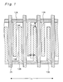
- Fig. 1 shows a schematic layout of a pair of opposed first electrodes and ribs in a plasma display device of Example 1 of the present invention.
- Fig. 2 is a schematic exploded perspective view of the plasma display device of Example 1.
- Fig. 3 shows a schematic layout of a pair of opposed first electrodes and ribs in a plasma display device of Example 2 of the present invention.
- Figs. 4A and 4B schematically show light emission states of glow discharge in a discharge cell.
- Figs. 5A and 5B schematically show light emission states of glow discharge in a discharge cell.
- Fig. 6 is a schematic exploded perspective view of a conventional plasma display device.
- Fig. 7 is a schematic layout of a pair of opposed electrodes and ribs in a conventional plasma display device.
- Fig. 8 is a variant of the schematic layout of a pair of opposed electrodes and ribs in the conventional plasma display device.
- Example 1 is concerned with the plasma display device of the present invention.
- Fig. 2 shows a schematic exploded perspective view of the plasma display device of Example 1.
- the plasma display device has a front panel 10 and a rear panel 20.
- the front panel 10 comprises a first substrate 11 composed, for example, of glass; a first electrode group constituted of a plurality of first electrodes formed on the first substrate 11; a dielectric layer 14 formed on the first electrode group and the first substrate 11; and a protective layer 15 formed on the dielectric layer 14.
- the dielectric layer 14 is composed of SiO 2 or a low-melting glass, and the protective layer 15 is composed of magnesium oxide (MgO).
- the rear panel 20 comprises a second substrate 21 composed, for example, of glass; a second electrode group constituted of a plurality of second electrodes (also called address electrodes or data electrodes) 22 formed on the second substrate 21 in the form of stripes; fluorescent layers 24 formed above the second electrodes 22; and ribs 25 formed between the adjacent second electrodes 22.
- a dielectric film 23 is formed on the second electrodes 22 and the second substrate 21.
- the ribs 25 are composed of an insulating material and are formed on regions which are on the dielectric film 23 and between the adjacent second electrodes 22, and the ribs 25 extend in parallel with the second electrodes 22.
- the fluorescent layer 24 is provided so as to be on, and to extend from, the dielectric film 23 and so as to be on side walls of the ribs 25.
- Each fluorescent layer 24 is constituted of a red fluorescent layer 24R, a green fluorescent layer 24G or a blue fluorescent layer 24B, and the fluorescent layers 24R, 24G and 24B of these colours are provided in a predetermined order.
- Fig. 2 is the exploded perspective view, and in the actual plasma display device, top portions of the ribs 25 of the rear panel 20 are in contact with the protective layer 15 of the front panel 10. Further, the front panel 10 and the rear panel 20 are arranged such that the protective layer 15 is opposed to the fluorescent layers 24, and the front panel 10 and the rear panel 20 are bonded to each other in their marginal portions with a seal layer (not shown). A region where a pair of main wirings 12A and 12B and a pair of branch electrodes 13A and 13B extending from the main wirings 12A and 12B overlap the second electrode 22 positioned between the adjacent two ribs 25 corresponds to a discharge cell.
- Ne-Xe mixed gases for example, 50 % Ne - 50 % Xe mixed gases
- a pressure of 8 x 10 4 Pa 0.8 atmospheric pressure
- Fig. 1 shows a schematic layout of a pair of opposing first electrodes and the ribs 25.
- a pair of the opposing first electrodes comprise (A) the first main wiring 12A, (B) the second main wiring 12B extending in parallel with the first main wiring 12A, (C) the first branch electrode 13A which extends between the adjacent ribs 25, extends from the first main wiring 12A toward the second main wiring 12B and extends short of the second main wiring 12B, and (D) the second branch electrode 13B which extends between the adjacent ribs 25, extends from the second main wiring 12B toward the first main wiring 12A and extends short of the first main wiring 12A such that the second branch electrode 13B is opposed to the first branch electrode 13A.
- the first electrode group is a set of the first main wiring 12A, the second main wiring 12B, the first branch electrode 13A and the second branch electrode 13B.
- the first branch electrodes 13A and the second branch electrodes 13B have a nearly rectangular form each, and the first branch electrodes 13A and the second branch electrodes 13B extend in parallel with one another. Further, the first main wiring 12A and the second main wiring 12B extend in parallel with each other, and the extending direction of these main wirings 12A and 12B and the extending direction of the ribs 25 make an angle, for example, of 90°.
- a region surrounded by dotted lines corresponds to one pixel.
- Each pixel has an outer form of a square, and each pixel is divided into three sections (cells) with the ribs 25.
- One section emits light of one of three primary colours (R,G,B).
- R,G,B primary colours
- each section has a dimension slightly smaller than (L 0 /3) x (L 0 ).
- those portions 13A' and 13B' of the branch electrodes 13A and 13B which contribute to discharging have a length close to (L 0 ).
- Each of the branch electrodes 13A and 13B is formed on the first substrate 11 and is composed of a transparent electrically conductive material such as ITO.
- a transparent electrically conductive material such as ITO.
- As an electrically conductive material for the first and second main wirings 12A and 12B there is used a material having a lower electric resistivity than ITO, such as a chromium/copper/chromium stacked layer.
- the first and second main wirings 12A and 12B have a line width which is made as small as possible (for example, 50 ⁇ m wide) so that the brightness of a display screen (upper side surface of the first substrate 11 in Fig. 2) is not impaired.
- a second electrode group is a set of second electrodes 22 formed on the second substrate 21 in the form of stripes.
- Each second electrode is composed, for example, of silver or aluminium.
- the second electrodes contribute to initiate discharge together with the first and second branch electrodes 13A and 13B, and also contribute to reflecting light emitted from the fluorescent layers 24 toward a display screen to improve the brightness of the display screen.
- Each fluorescent layer 24 is constituted of a red fluorescent layer 24R, a green fluorescent layer 24G or a blue fluorescent layer 24B, and these fluorescent layers 24R, 24G and 24B which emit light of three primary colours constitute one combination, and the fluorescent layers are formed on the second electrodes 22 in a predetermined order.
- a pulse voltage higher than a discharge initiation voltage V bd is applied to all of the first main wirings 12A for a short period of time, whereby discharging takes place, a wall charge is generated on the surface of the dielectric layer 14 near one of the branch electrodes due to dielectric polarisation, the wall charge is accumulated, and an apparent discharge initiation voltage decreases.
- a voltage is applied to the second electrodes (address electrodes) 22, a voltage is applied to one of the main wirings included in cells which are allowed not to display, whereby discharging is caused between the second electrode 22 and one of the branch electrodes, to erase the accumulated wall charge.
- This erasing discharge is consecutively carried out in the second electrodes 22. Meanwhile, no voltage is applied to one of the main wirings included in cells which are allowed to display, whereby the accumulation of the wall charge is retained. Then, a predetermined pulse voltage is applied between all of pairs of the main wirings 12A and 12B. As a result, in the cells where the accumulation of the wall charge is retained, discharging is initiated between a pair of the branch electrodes 13A and 13B, and in such discharge cells, the fluorescent layers excited by irradiation with vacuum ultraviolet light generated by glow discharge in the rare gas emit characteristic light depending upon the fluorescent materials. Phases of discharge sustain voltages applied to one of the main wirings and the other of the main wirings deviate from each other by half a cycle, and the polarity of the electrodes is reversed depending upon the frequency of alternate current.
- a region where one of the main wirings and the second electrode 22 to which the pulse voltage is applied overlap is selected as a display pixel, and in the overlap region, the wall charge is generated on the surface of the dielectric layer 14 due to dielectric polarisation, whereby the wall charge is accumulated.
- a discharge sustain voltage V sus lower than V bd is applied to a pair of the main wirings 12A and 12B.
- the fluorescent layer 24 is excited by being irradiated with vacuum ultraviolet light radiated due to the excitation of the rare gas generated in the space, and the fluorescent layer 24 emits characteristic light depending upon the fluorescent material.
- the length of the electrodes which contribute to discharging i.e., lengths of opposed portions of a pair of the branch electrodes 13A and 13B
- the length of the counterparts of any conventional plasma display device is longer than the length of the counterparts of any conventional plasma display device, so that the area of the discharge region can be remarkably increased as compared with any conventional tri-electrode type AC driven type plasma display device shown in Figs. 6 to 8.
- the brightness of the display screen can be increased.
- the method of producing the plasma display device of Example 1 will be outlined below.
- the first substrate 11, all the structures formed thereon, the second substrate 21, or all the structures formed thereon at any stage is sometimes referred to as "substratum”.
- the front panel 10 can be produced as follows. First, an ITO layer is formed on the entire surface of the first substrate 11, for example, by a sputtering method, and the ITO layer is patterned in the form of stripes by photolithography and an etching method, whereby the first and second branch electrodes 13A and 13B can be formed. Then, a chromium/copper/chromium stacked layer is formed on the entire surface of the substratum, for example, by a sputtering method, and the chromium/copper/chromium stacked layer is patterned by photolithography and an etching method, whereby the first and second main wirings 12A and 12B can be formed.
- each of the first branch electrodes 13A and the first main wiring 12A overlap each other, and one end portion of each of the second branch electrodes 13B and the second main wiring 12B overlap each other.
- the dielectric layer 14 which has a thickness of approximately 10 ⁇ m, is formed on the entire surface of the substratum, and then the protective layer 15 composed of MgO, which has a thickness of approximately 0.6 ⁇ m, is formed on the dielectric layer 14.
- the dielectric layer 14 can be formed, for example, by forming a low-melting glass paste layer on the entire surface of the substratum by a screen printing method and calcining or sintering the low-melting glass paste layer.
- the protective layer 15 can be formed, for example, by forming a magnesium oxide layer on the entire surface of the dielectric layer 14 by an electron beam deposition method. According to the above steps, the front panel 10 can be completed.
- the rear panel 20 can be produced as follows. First, a silver paste is printed in the form of stripes on the second substrate 21, for example, by a screen printing method, and the printed silver paste is calcined or sintered, whereby the second electrodes 22 can be formed. Then, a low-melting glass paste layer is formed on the entire surface of the substratum by a screen printing method, and the low-melting glass paste layer is calcined or sintered, whereby the dielectric film 23 is formed. Then, a low-melting glass paste layer is printed on the dielectric film above each region between the adjacent second electrodes 22, for example, by a screen printing method, and the low-melting glass paste layer is calcined or sintered, to form the ribs 25.
- the height of the ribs can be, for example, 1 x 10 -4 m (100 ⁇ m) to 2 x 10 -4 m (200 ⁇ m). Then, fluorescent slurries of three primary colours are consecutively printed, followed by calcining or sintering, to form the fluorescent layers 24R, 24G and 24B. According to the above step, the rear panel 20 can be completed.
- the plasma display device is assembled.
- a seal layer (not shown) is formed on a marginal portion of the rear panel 20, for example, by a screen printing method.
- the front panel 10 and the rear panel 20 are attached to each other, followed by calcining or sintering, to cure the seal layer.
- the space formed between the front panel 10 and the rear panel 20 is vacuumed, and then, Ne-Xe mixed gases (for example, 50 % Ne - 50 % Xe mixed gases) are charged at a pressure of 8 x 10 4 Pa (0.8 atmospheric pressure) and sealed in the space, to complete the plasma display device.
- Ne-Xe mixed gases for example, 50 % Ne - 50 % Xe mixed gases
- Example 2 is a variant of Example 1.
- Example 2 differs from Example 1 in that the comers of top portion of each of the first branch electrodes 13A and the comers of top portion of each of the second branch electrodes 13B are rounded as shown in Fig. 3 showing a schematic layout of the first electrodes and the ribs 25.
- the first branch electrodes 13A and the second branch electrodes 13B have the form of a rectangle each when macroscopically viewed as a plan view.
- the plasma display device of Example 2 can be structured and constituted similarly to the plasma display device of Example 1 except for the above point, so that detailed explanations thereof are omitted.
- a second electrode group constituted of a plurality of second electrodes may be formed on the first substrate. That is, there may be employed a constitution in which the second electrodes are formed on the dielectric layer 14 through an insulating film and the extending direction of the second electrodes and the extending direction of each main wiring make a predetermined angle (for example, 90°).
- the first branch electrode and the second branch electrode extend from main wirings so as to go counter to each other, so that those portions of the electrodes which contribute to discharging can have a sufficient length each. Therefore, the discharge regions thereof can be broadened, so that there can be overcome the problem that the brightness of a plasma display device decreases in spite of a simple structure.
Landscapes
- Engineering & Computer Science (AREA)
- Physics & Mathematics (AREA)
- Plasma & Fusion (AREA)
- Chemical & Material Sciences (AREA)
- Materials Engineering (AREA)
- Gas-Filled Discharge Tubes (AREA)
- Transforming Electric Information Into Light Information (AREA)
Applications Claiming Priority (2)
| Application Number | Priority Date | Filing Date | Title |
|---|---|---|---|
| JP28963799 | 1999-10-12 | ||
| JP28963799A JP2001110324A (ja) | 1999-10-12 | 1999-10-12 | プラズマ表示装置 |
Publications (1)
| Publication Number | Publication Date |
|---|---|
| EP1093148A1 true EP1093148A1 (fr) | 2001-04-18 |
Family
ID=17745824
Family Applications (1)
| Application Number | Title | Priority Date | Filing Date |
|---|---|---|---|
| EP00402827A Withdrawn EP1093148A1 (fr) | 1999-10-12 | 2000-10-12 | Dispositif d'affichage à plasma |
Country Status (5)
| Country | Link |
|---|---|
| EP (1) | EP1093148A1 (fr) |
| JP (1) | JP2001110324A (fr) |
| KR (1) | KR20010067319A (fr) |
| CN (1) | CN1308358A (fr) |
| TW (1) | TW466527B (fr) |
Cited By (2)
| Publication number | Priority date | Publication date | Assignee | Title |
|---|---|---|---|---|
| EP1130619A2 (fr) * | 2000-01-12 | 2001-09-05 | Sony Corporation | Dispositif d'affichage à plasma |
| US7755285B2 (en) | 2004-11-30 | 2010-07-13 | Fujitsu Hitachi Plasma Display Limited | Plasma display panel and plasma display apparatus |
Families Citing this family (4)
| Publication number | Priority date | Publication date | Assignee | Title |
|---|---|---|---|---|
| KR100669391B1 (ko) | 2005-03-18 | 2007-01-15 | 삼성에스디아이 주식회사 | 플라즈마 디스플레이 패널 |
| KR100722263B1 (ko) * | 2005-11-04 | 2007-05-28 | 엘지전자 주식회사 | 플라즈마 디스플레이 패널 |
| JPWO2009034601A1 (ja) * | 2007-09-12 | 2010-12-16 | 株式会社日立製作所 | プラズマディスプレイパネル |
| WO2010026617A1 (fr) * | 2008-09-04 | 2010-03-11 | 日立プラズマディスプレイ株式会社 | Panneau d'affichage à plasma, unité de panneau d'affichage à plasma, et procédé de fabrication de panneau d'affichage à plasma |
Citations (6)
| Publication number | Priority date | Publication date | Assignee | Title |
|---|---|---|---|---|
| US5066890A (en) * | 1989-06-23 | 1991-11-19 | Thomson Tubes Electroniques | Plasma panels in delimited discharge zones |
| EP0580868A1 (fr) * | 1992-02-06 | 1994-02-02 | Noritake Co., Limited | Panneau d'affichage a plasma |
| JPH11126561A (ja) * | 1997-08-19 | 1999-05-11 | Matsushita Electric Ind Co Ltd | ガス放電パネル |
| US5962974A (en) * | 1996-10-04 | 1999-10-05 | Pioneer Electronic Corporation | Face-discharge AC driving plasma display panel |
| EP0996138A2 (fr) * | 1998-10-23 | 2000-04-26 | Sony Corporation | Dispositif d'affichage plat à décharge plasma et procédé de commande dudit dispositif |
| EP1024516A1 (fr) * | 1997-08-19 | 2000-08-02 | Matsushita Electronics Corporation | Panneau d'affichage a decharge gazeuse |
-
1999
- 1999-10-12 JP JP28963799A patent/JP2001110324A/ja active Pending
-
2000
- 2000-10-11 KR KR1020000059852A patent/KR20010067319A/ko not_active Withdrawn
- 2000-10-11 TW TW089121148A patent/TW466527B/zh not_active IP Right Cessation
- 2000-10-12 CN CN00131861A patent/CN1308358A/zh active Pending
- 2000-10-12 EP EP00402827A patent/EP1093148A1/fr not_active Withdrawn
Patent Citations (6)
| Publication number | Priority date | Publication date | Assignee | Title |
|---|---|---|---|---|
| US5066890A (en) * | 1989-06-23 | 1991-11-19 | Thomson Tubes Electroniques | Plasma panels in delimited discharge zones |
| EP0580868A1 (fr) * | 1992-02-06 | 1994-02-02 | Noritake Co., Limited | Panneau d'affichage a plasma |
| US5962974A (en) * | 1996-10-04 | 1999-10-05 | Pioneer Electronic Corporation | Face-discharge AC driving plasma display panel |
| JPH11126561A (ja) * | 1997-08-19 | 1999-05-11 | Matsushita Electric Ind Co Ltd | ガス放電パネル |
| EP1024516A1 (fr) * | 1997-08-19 | 2000-08-02 | Matsushita Electronics Corporation | Panneau d'affichage a decharge gazeuse |
| EP0996138A2 (fr) * | 1998-10-23 | 2000-04-26 | Sony Corporation | Dispositif d'affichage plat à décharge plasma et procédé de commande dudit dispositif |
Cited By (2)
| Publication number | Priority date | Publication date | Assignee | Title |
|---|---|---|---|---|
| EP1130619A2 (fr) * | 2000-01-12 | 2001-09-05 | Sony Corporation | Dispositif d'affichage à plasma |
| US7755285B2 (en) | 2004-11-30 | 2010-07-13 | Fujitsu Hitachi Plasma Display Limited | Plasma display panel and plasma display apparatus |
Also Published As
| Publication number | Publication date |
|---|---|
| TW466527B (en) | 2001-12-01 |
| CN1308358A (zh) | 2001-08-15 |
| JP2001110324A (ja) | 2001-04-20 |
| KR20010067319A (ko) | 2001-07-12 |
Similar Documents
| Publication | Publication Date | Title |
|---|---|---|
| US6965200B2 (en) | Plasma display device having barrier ribs | |
| US6657396B2 (en) | Alternating current driven type plasma display device and method for production thereof | |
| US6541922B2 (en) | Alternating current driven type plasma display device and method for the production thereof | |
| US6628077B2 (en) | Alternating current driven type plasma display | |
| US6713958B2 (en) | Alternating current driven type plasma display device | |
| US6469451B2 (en) | Alternating-current-driven-type plasma display | |
| JP2002203487A (ja) | 交流駆動型プラズマ表示装置 | |
| EP1093148A1 (fr) | Dispositif d'affichage à plasma | |
| KR101128671B1 (ko) | 교류 구동형 플라즈마 표시장치 및 그 제조방법 | |
| US20020180355A1 (en) | Plasma display device | |
| US6737805B2 (en) | Plasma display device and method of producing the same | |
| JP4052050B2 (ja) | 交流駆動型プラズマ表示装置 | |
| JP2004071219A (ja) | プラズマ表示装置 | |
| US20040038615A1 (en) | Production method for plasma display panel unit-use panel and production method for plasma display unit | |
| JP2004186062A (ja) | プラズマ表示装置 | |
| JP4114384B2 (ja) | プラズマ表示装置 | |
| JP2001076630A (ja) | 交流駆動型プラズマ表示装置 | |
| JP2001266758A (ja) | プラズマ表示装置及びその製造方法 | |
| JP2003045341A (ja) | プラズマ放電表示装置 | |
| JP2001076628A (ja) | プラズマ表示装置 | |
| JP2004178880A (ja) | プラズマ表示装置 | |
| JP2004071218A (ja) | プラズマ表示装置 |
Legal Events
| Date | Code | Title | Description |
|---|---|---|---|
| PUAI | Public reference made under article 153(3) epc to a published international application that has entered the european phase |
Free format text: ORIGINAL CODE: 0009012 |
|
| AK | Designated contracting states |
Kind code of ref document: A1 Designated state(s): DE FR GB |
|
| AX | Request for extension of the european patent |
Free format text: AL;LT;LV;MK;RO;SI |
|
| 17P | Request for examination filed |
Effective date: 20010801 |
|
| AKX | Designation fees paid |
Free format text: DE FR GB |
|
| 17Q | First examination report despatched |
Effective date: 20040429 |
|
| STAA | Information on the status of an ep patent application or granted ep patent |
Free format text: STATUS: THE APPLICATION IS DEEMED TO BE WITHDRAWN |
|
| 18D | Application deemed to be withdrawn |
Effective date: 20040504 |