EP1093219A1 - Schaltungsanordnung zur Demodulation eines Zwischenfrequenz-Videosignals - Google Patents
Schaltungsanordnung zur Demodulation eines Zwischenfrequenz-Videosignals Download PDFInfo
- Publication number
- EP1093219A1 EP1093219A1 EP00203417A EP00203417A EP1093219A1 EP 1093219 A1 EP1093219 A1 EP 1093219A1 EP 00203417 A EP00203417 A EP 00203417A EP 00203417 A EP00203417 A EP 00203417A EP 1093219 A1 EP1093219 A1 EP 1093219A1
- Authority
- EP
- European Patent Office
- Prior art keywords
- polarity
- signal
- inverter
- video signal
- video
- Prior art date
- Legal status (The legal status is an assumption and is not a legal conclusion. Google has not performed a legal analysis and makes no representation as to the accuracy of the status listed.)
- Granted
Links
- 230000008859 change Effects 0.000 description 6
- 238000000034 method Methods 0.000 description 4
- 230000001052 transient effect Effects 0.000 description 4
- 230000007704 transition Effects 0.000 description 4
- 230000001960 triggered effect Effects 0.000 description 4
- 230000008901 benefit Effects 0.000 description 3
- 238000010586 diagram Methods 0.000 description 3
- 230000008569 process Effects 0.000 description 3
- 230000010355 oscillation Effects 0.000 description 2
- 230000004044 response Effects 0.000 description 2
- 230000006978 adaptation Effects 0.000 description 1
- 230000001419 dependent effect Effects 0.000 description 1
- 230000000694 effects Effects 0.000 description 1
- 230000010363 phase shift Effects 0.000 description 1
- 230000001360 synchronised effect Effects 0.000 description 1
- 230000029305 taxis Effects 0.000 description 1
Images

Classifications
-
- H—ELECTRICITY
- H03—ELECTRONIC CIRCUITRY
- H03D—DEMODULATION OR TRANSFERENCE OF MODULATION FROM ONE CARRIER TO ANOTHER
- H03D1/00—Demodulation of amplitude-modulated oscillations
- H03D1/22—Homodyne or synchrodyne circuits
- H03D1/2245—Homodyne or synchrodyne circuits using two quadrature channels
- H03D1/2254—Homodyne or synchrodyne circuits using two quadrature channels and a phase locked loop
-
- H—ELECTRICITY
- H04—ELECTRIC COMMUNICATION TECHNIQUE
- H04N—PICTORIAL COMMUNICATION, e.g. TELEVISION
- H04N21/00—Selective content distribution, e.g. interactive television or video on demand [VOD]
- H04N21/40—Client devices specifically adapted for the reception of or interaction with content, e.g. set-top-box [STB]; Operations thereof
- H04N21/41—Structure of client; Structure of client peripherals
- H04N21/426—Internal components of the client ; Characteristics thereof
-
- H—ELECTRICITY
- H04—ELECTRIC COMMUNICATION TECHNIQUE
- H04N—PICTORIAL COMMUNICATION, e.g. TELEVISION
- H04N21/00—Selective content distribution, e.g. interactive television or video on demand [VOD]
- H04N21/40—Client devices specifically adapted for the reception of or interaction with content, e.g. set-top-box [STB]; Operations thereof
- H04N21/43—Processing of content or additional data, e.g. demultiplexing additional data from a digital video stream; Elementary client operations, e.g. monitoring of home network or synchronising decoder's clock; Client middleware
- H04N21/438—Interfacing the downstream path of the transmission network originating from a server, e.g. retrieving encoded video stream packets from an IP network
- H04N21/4382—Demodulation or channel decoding, e.g. QPSK demodulation
-
- H—ELECTRICITY
- H04—ELECTRIC COMMUNICATION TECHNIQUE
- H04N—PICTORIAL COMMUNICATION, e.g. TELEVISION
- H04N5/00—Details of television systems
- H04N5/44—Receiver circuitry for the reception of television signals according to analogue transmission standards
- H04N5/455—Demodulation-circuits
Definitions
- the invention relates to a circuit arrangement for demodulating an intermediate frequency video signal with a video demodulator and with a Costas loop trained phase locked loop, with an output signal of one in the Costas loop provided controllable oscillator and the intermediate frequency video signal on the Video demodulator are coupled.
- Circuitry for demodulating intermediate frequency video signals generally with a phase locked loop to recover the modulation frequency the correct phase position.
- Conventional phase locked loops which only unite every 360 ° have a stable operating point, react to overmodulation of the amplitude-modulated TV picture carrier with a phase shift by 180 °. Through this phase change transitional the synchronous relationship between the phase of the phase locked loop delivered signal and the demodulator disturbed. Image disturbances occur.
- a polarity inverter which is connected downstream of the video demodulator and by means of which the polarity of the demodulated video signal can be inverted as a function of a control signal supplied by a polarity detector, and that the polarity detector determines the polarity of the output signal of the video demodulator or of the polarity inverter and, depending on the determined polarity, controls the polarity inverter by means of the control signal such that the demodulated video signal has a predetermined polarity at the output of the polarity inverter.
- a polarity inverter is provided in the circuit for demodulating an intermediate frequency video signal. This is downstream of the video demodulator and allows the polarity of the demodulated provided by the video demodulator Invert video signal. So it can basically be done by means of this polarity inverter a desired polarity of the demodulated video signal can be established.
- the polarity inverter is controlled by means of a control signal which is generated by a Polarity detector is supplied.
- the polarity detector represents the polarity of the output signal from either the video demodulator or the polarity inverter and controls the polarity inverter in Dependency of this determined polarity so that the demodulated video signal on Output of the polarity inverter has a predetermined polarity.
- the basic idea of the invention is therefore the actual polarity of the demodulated one Determine video signal and depending on this determined polarity To control polarity inverter so that at the output of the circuit arrangement demodulated video signal with the desired polarity occurs.
- An embodiment of the invention provided according to claim 2 has above all that Advantage that if the polarity detector detects the polarity of the output signal of the Polarity inverter detects a type (and not that of the output signal of the demodulator) feedback solution is possible, in which in the polarity detector when the unwanted occurs Polarity of the demodulated video signal changes status only once of the control signal must be triggered, since with the switching of the trigger triggered thereby Polarity inverter then outputs the video signal at its output in the correct desired polarity occurs.
- the circuit arrangement is advantageous as in a further embodiment provided according to claim 3 designed so that the demodulated video signal with negative Polarity occurs.
- the demodulated video signal is usually used in known circuit arrangements processed in this polarity.
- the one-time response of the polarity detector when a occurs unwanted polarity can be advantageous, as in a further embodiment of the Invention according to claim 4 is provided by means of a comparator and a D flip-flop be achieved.
- the comparator then delivers when the video signal supplied to it amount exceeds the value of a comparison signal, a corresponding pulse to the D flip-flop.
- the D flip-flop changes its switching state and hence the control signal its state.
- the polarity inverter then switches over and the demodulated video signal now occurs behind the polarity inverter in the desired polarity. Therefore, the comparator does not subsequently Switching impulse triggered more.
- the comparison voltage advantageously has about half the value the voltage that occurs in the video signal at maximum modulation. This applies for both positive and negative polarity.
- this modulation type signal can also be used for the polarity detector notify the type of modulation and accordingly the polarity inverter Taxes. It can be achieved with both negative modulation and with positive modulation, the circuit arrangement is always demodulated, for example Has negative polarity video signal.
- the measures according to claim 8 are advantageously provided according to a further embodiment of the invention.
- the switchable inverter may or may not invert the polarity of the demodulated video signal supplied to the polarity detector. The result of this is that the polarity detector always switches the polarity inverter so that the demodulated video signal appears at its output with a fixed, desired polarity, which is independent of what type of modulation the intermediate frequency video signal was.
- a DC voltage position of the demodulated video signal which varies depending on the type of modulation, is compensated for by the video amplifier.
- the reference voltage instead of the switchable inverter of the comparator depending on the type of modulation of the intermediate frequency video signal to change.
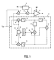
- FIG. 1 shows in the form of a block diagram a circuit arrangement according to the invention for demodulating an intermediate frequency video signal, which has a video demodulator 1 to which the intermediate frequency video signal V ZF is fed.
- the video demodulator 1 receives the modulation frequency and oscillator frequency from a wide Costas loop 5, which is explained below, and which serves as a phase locked loop.
- the video demodulator 1 is followed by a polarity inverter 2, which is controlled by a polarity detector 3 by means of a control signal.
- the polarity detector 3 receives the output signal of the polarity inverter 2 and a modulation type signal MS indicating the type of demodulation of the intermediate frequency video signal V IF .
- the polarity inverter 2 is followed by a video amplifier 4, the DC voltage gain of which can be changed as a function of the modulation type signal MS. The DC voltage value can thus be set in the output signal of the amplifier 4.
- the video amplifier 4 delivers the output signal of the output side of the invention Circuit arrangement, that is, the demodulated video signal in a desired polarity.
- the Costas loop 5 also receives the intermediate frequency video signal V ZF on the input side, which is fed to two mixers 6 and 7 provided in it.
- the first mixer 6 is followed by a first low-pass filter 8, which in turn is a Limiter 9 is connected downstream, its output signal to a first multiplier 10 is led.
- the output signal of the first multiplier 10 reaches a loop filter 11, which is followed by a controllable oscillator 12.
- the controllable oscillator 12 provides a first output with a signal with zero phase position, which the video demodulator 1 is supplied.
- the controllable delivers at a second output 14 Oscillator an output signal shifted in phase by 90 ° compared to the first input 1, which reaches the second mixer 7.
- the second mixer 7 is a second low-pass filter 15 connected, its output signal to the first multiplier 10 arrives.
- the basic mode of operation of such a Costas loop is from the above Publication known.
- the first mixer 6, the first low-pass filter 8 and the Limiters 9 form a so-called I-arm in the Costas Loop, whereas the second Mixer 7 and the second low-pass filter 15 form a so-called Q-arm.
- the Q arm is the one who works like a normal PLL.
- the I-arm delivers a signal which occurs in quadrature against the signal of the Q-arm. With that the tension of the Q-arm inverted in the first multiplier 10 whenever the polarity of the Q-arm supplied signal inverted. This always occurs when the modulation is yours
- the algebraic sign changes, if the Costas Loop is at a working point offset by 180 ° regulates. The result of this structure of the Costas Loop is that it has stable working points offset by 180 ° to one another
- the Costas loop can then continue to be stable at the modulation frequency of one of its supplied intermediate frequency video signal regulate when the phase of this modulation frequency jumps by 180 ° due to overmodulation.
- the Costas Loop snaps in such a jump to the new phase position offset by 180 ° immediately. It no or at least no significant transient transitions occur. The occurs Effect that the tapped at the first output 13 of the controllable oscillator 12 Signal that is supplied to the video demodulator 1 during the times when Overmodulation occurs by 180 ° in phase with respect to the modulation signal is offset.
- the Costas loop there is also a third low-pass filter 16 and a second multiplier 17 provided, on the one hand the output signal of the third low-pass filter 16 and that of the second low-pass filter 15 of the Q-arm are supplied.
- the output signal of the second multiplier 17 and the first multiplier 10 are by means of an overlay stage 18 superimposed and fed to the loop filter 11.
- the elements 16 and 17 form a type of frequency detector, which serves the operating frequency the Costas loop and thus also the controllable oscillator 12 at a relative large frequency deviation from the modulation frequency. she ran namely a frequency-dependent signal, which regardless of the phase position the operating frequency of the Costas Loop adjusts to a frequency deviation.
- the Costas Loop 5 can be set to a working point that is offset by 180 ° rest. For the output signal of the video demodulator 1, this has the consequence that this has an undesirable polarity. This is due to the circuit arrangement according to the invention be avoided.
- the polarity inverter 2 and the polarity detector 3 are provided.
- the Polarity inverter 2 can determine the polarity of the demodulated video signal supplied to it be inverted. This happens depending on the control signal from the polarity detector 3 is delivered.
- the polarity detector 3 represents the polarity of the output signal of the polarity inverter 2 and controls it depending on the control signal so that this output signal always has a desired polarity, for example a negative one Polarity.
- the output of the polarity inverter 2 thus always delivers a demodulated video signal with the desired polarity.
- the polarity of the output signal of the circuit arrangement or of the polarity inverter 2 is therefore independent of which of two working points offset by 180 ° to each other the Costas Loop 5 has locked.
- the circuit arrangement according to the invention shown in the embodiment of FIG. 1 is also suitable for different intermediate frequency video signals Process modulation types.
- signals can be positive or negative modulation occur.
- the polarity detector 3 is given an indication of the type of modulation Modulation type signal MS supplied. Depending on this signal, the Polarity detector 3 when generating the control signal, the type of modulation that occurs. This ensures that the demodulated video signal is independent of the type of modulation always has a desired polarity at the output of the polarity inverter 2.
- the modulation type signal MS is also a Amplifier 4 supplied, which the output signal of the polarity inverter 2 by a in Dependency of the modulation type signal MS adjustable DC voltage gain so amplifies that on the output side always a video signal with approximately the same DC voltage value occurs.
- the circuit arrangement according to the invention not only with overmodulation, but also with intermediate frequency video signals of various Modulation type always a demodulated one on the output side without transient disturbances Video signal of a desired polarity and with a fixed DC voltage position supplies.
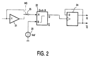
- FIG. 2 shows circuit elements of the polarity detector 3 in more detail Circuit arrangement according to FIG. 1
- the output signal of the polarity inverter 2 of the arrangement according to FIG. 1 becomes within of the polarity detector 3 in the detailed illustration according to FIG. 2 on the one hand Inverter 21 and on the other hand, a switch 25 is supplied.
- This switch 25 is in Dependency of the modulation type signal MS switched so that it is positive modulation of the intermediate frequency video signal on the output of the inverter 21 and at negative modulation type is connected to the input signal of the polarity detector.
- the output signal of the polarity inverter supplied to the polarity detector 3 2 then inverted by means of the inverter 21 when the intermediate frequency video signal positive modulation type. If it has a negative modulation type, the output signal of the polarity inverter 2 is not inverted.
- Your switch 25 is followed by a comparator 22, at the input A of which Switch 25 supplied signal is guided.
- a second input B of the comparator 22 a comparison signal Vref is supplied, which is supplied by a voltage source 23.
- the comparator 22 then delivers an output signal at its output Q when that is on its first input A from the switch 25 signal is greater than his second input B supplied comparison signal Vref.
- the signal appearing at the Q output of the comparator 22 becomes a switching input A downstream D flip-flop 24 is supplied, the output signal Q 'of the D input this D flip-flop 24 is fed back. It is thereby achieved that the D flip-flop 24 its switching state changes when in the output signal Q of the comparator 22 Low-high transition occurs, that is to say in the transition zone in which the comparator 22 determines that the input signal at its input A is greater than that at its input B.
- the output signal Q of the D flip-flop 24 represents the control signal which is in the circuit arrangement 1, the polarity inverter 2 is supplied.
- the control signal that is fed to the polarity inverter 2 is achieved a change in the polarity of the polarity inverter 2 specifies whenever the comparator 22 determines that the video signal has the amplitude of the comparison signal Vref exceeds. If the value of the comparison signal is set so that an exceeding of its value only occurs when a signal of undesired polarity occurs, that is it Objective of the circuit arrangement according to the invention achieved; then it will always be if the polarity of the demodulated video signal is incorrect at the output of the polarity inverter 2 the control signal switched so that this output signal again the desired Has polarity.
- the waveforms A and B represent those of a demodulated video signal which was obtained from an intermediate frequency video signal with a positive modulation type.
- the oscillation train A of the demodulated video signal shows how it can occur, for example, at the output of the video demodulator 1 or also the polarity inverter 2 of the circuit arrangement according to FIG. 1 (or at the input of the comparator 22 of FIG. 3). This oscillation train shows negative polarity in the desired way.
- FIG. 3 shows that the waveform of the video signal B, which is an unwanted Has polarity, temporarily exceeds the comparison signal Vref. In the arrangement 2, this would have the consequence that a in the output signal Q of the comparator 22 Low-high transition occurs, which in turn switches the state of the D flip-flop 24 would have resulted.
- the control signal which in the arrangement according to FIG. 1 is supplied to the polarity inverter 2, switched accordingly. this in turn would result in the polarity inverter being switched over and the polarity of it supplied demodulated video signal inverted.
- Fig. 3 also shows two waveforms C and D, the demodulated video signals of an intermediate frequency video signal in negative modulation.
- the inverter 21 Since in the circuit arrangement according to FIG. 2, the inverter 21 only with such intermediate frequency video signals is active, the positive modulation type, the signals occur C and D, the demodulated video signals of an intermediate frequency video signal more negative Modalions originate in the opposite polarity.
- the vibration train D shows the demodulated intermediate frequency video signal of desired negative polarity one Intermediate frequency video signal with negative modulation.
- the shows Vibration train C a demodulated video signal of undesirable positive polarity.
- the comparison voltage Vref is exceeded by the signal of the Vibration train C a switching of the D flip-flop 24 and thus the one supplied by him Triggers control signal, so that the polarity inverter 2 an inversion of him supplied demodulated video signal makes so that the signal back in the desired negative polarity corresponding to D occurs.
- the your delivered demodulated video signal always has a desired polarity without Transient disturbances in the event of a possible occurrence in the intermediate frequency video signal Overmodulation. It is also independent of which of two around 180 ° offset working points Costas-Loop snaps. In addition, even one Adaptation to the different types of modulation of the intermediate frequency video signal be provided so that the polarity of the demodulated video signal supplied even from is independent of the type of modulation.
Landscapes
- Engineering & Computer Science (AREA)
- Multimedia (AREA)
- Signal Processing (AREA)
- Power Engineering (AREA)
- Stabilization Of Oscillater, Synchronisation, Frequency Synthesizers (AREA)
Abstract
Description

und dass der Polaritätsdetektor die Polarität des Ausgangssignals des Video-Demodulators oder des Polaritätsinverters feststellt und in Abhängigkeit der festgestellten Polarität den Polaritätsinverter mittels des Steuersignals so ansteuert, dass das demodulierte Videosignal am Ausgang des Polaritätsinverters eine vorgegebene Polarität aufweist.
Darüber hinaus wird mittels des Videoverstärkers eine je nach Modulationsart variierende Gleichspannungslage des demodulierten Videosignals ausgeglichen.
Dem Polaritätsinverter 2 ist ein Video-Verstärker 4 nachgeschaltet, dessen Gleichspannungsverstärkung in Abhängigkeit des Modulationsartsignals MS veränderbar ist. Somit ist der Gleichspannungswert in dem Ausgangssignal des Verstärkers 4 einstellbar.
Dabei zeigt der Schwingungszug A des demodulierten Videosignals wie er beispielsweise am Ausgang des Video-Demodulators 1 bzw. auch Polaritätsinverters 2 der Schaltungsanordnung gemäß Fig. 1 (bzw. am Eingang des Komparators 22 der Fig.3) auftreten kann. Dieser Schwingungszug zeigt in gewünschter Weise negative Polarität.
Claims (10)
- Schaltungsanordnung zur Demodulation eines Zwischenfrequenz-Videosignals mit einem Video-Demodulator (1) und mit einem als Costas-Loop ausgebildeten Phasenregelkreis (5), wobei ein Ausgangssignal eines in der Costas-Loop vorgesehenen steuerbaren Oszillators (12) und das Zwischenfrequenz-Videosignal auf den Video-Demodulator (1) gekoppelt sind,
dadurch gekennzeichnet,dass ein Polaritätsinverter (2) vorgesehen ist, der dem Video-Demodulator (1) nachgeschaltet ist und mittels dessen in Abhängigkeit eines von einem Polaritätsdetektor (3) gelieferten Steuersignals die Polarität des demodulierten Videosignals invertierbar ist, und dass der Polaritätsdetektor (3) die Polarität des Ausgangssignals des Video-Demodulators (1) oder des Polaritätsinverters (2) feststellt und in Abhängigkeit der festgestellten Polarität den Polaritätsinverter (2) mittels des Steuersignals so ansteuert, dass das demodulierte Videosignal am Ausgang des Polaritätsinverters (2) eine vorgegebene Polarität aufweist. - Schaltungsanordnung nach Anspruch 1,
dadurch gekennzeichnet,dass der Polaritätsdetektor (3) die Polarität des Ausgangssignals des Polaritätsinverters (2) feststellt. - Schaltungsanordnung nach Anspruch 1 oder 2,
dadurch gekennzeichnet,dass der Polaritätsdetektor (3) den Polaritätsinverter (2) so ansteuert,dass das Ausgangssignal des Polaritätsinverters (2) eine negative Polarität aufweist. - Schaltungsanordnung nach Anspruch 2,
dadurch gekennzeichnet,dass der Polaritätsdetektor (3) einen Komparator (22) aufweist, der dann, wenn das ihm zugeführte Videosignal betragsmäßig den Wert eines dem Komparator (22) zugeführten Vergleichssignals überschreitet, einen Impuls an ein D-Flip-Flop (24) gibt, welches auf diesen Impuls hin seinen Schaltzustand ändert, in Abhängigkeit dessen das Steuersignal generiert wird. - Schaltungsanordnung nach Anspruch 4,
dadurch gekennzeichnet,dass die Vergleichsspannung etwa den halben Wert der bei maximaler Modulation in einem Videosignal unerwünschter Polarität auftretenden Spannung aufweist. - Schaltungsanordnung nach Anspruch 1 oder 2,
dadurch gekennzeichnet,dass der Polaritätsinverter (3) als Multiplizierer ausgebildet ist. - Schaltungsanordnung nach Anspruch 1 oder 2,
dadurch gekennzeichnet,dass der Anordnung ein Modulationsart-Signal zugeführt wird, welches angibt, ob das Videosignal positiv oder negativ moduliert ist unddass der Polaritätsdetektor (3) das Steuersignal unter Berücksichtigung der Modulationsart generiert. - Schaltungsanordnung nach den Ansprüchen 4 und 7,
dadurch gekennzeichnet,dass das Videosignal in dem Polaritätsdetektor (3) einem schaltbaren Inverter (21;25) zugeführt wird, welcher in Abhängigkeit des Modulationsart-Signals angesteuert wird und dessen Ausgangssignal auf den Komparator (22) gekoppelt ist unddass dem Polaritätsinverter (2) ein Video-Verstärker (4) nachgeschaltet ist, dessen Gleichspannungsverstärkung in Abhängigkeit des Modulationsart-Signals veränderbar ist. - Schaltungsanordnung nach den Ansprüchen 4 und 7,
dadurch gekennzeichnet,dass der Wert der Vergleichsspannung in Abhängigkeit des Wertes des Modulationsart-Signals verändert wird und dass dem Polaritätsinverter (2) ein Video-Verstärker (4) nachgeschaltet ist, dessen Gleichspannungsverstärkung in Abhängigkeit des Modulationsart-Signals veränderbar ist. - Schaltungsanordnung nach den Ansprüchen 2, 3, 4, 5 und 8,
dadurch gekennzeichnet,dass die Vergleichsspannung eine positive Polarität aufweist und dass das Ausgangssignal des Polaritätsinverters (2) vor Kopplung auf den Komparator (22) nur dann mittels des schaltbaren Inverters (21) invertiert wird, wenn das Modulationsart-Signal ein positiv moduliertes Videosignal indiziert.
Applications Claiming Priority (2)
| Application Number | Priority Date | Filing Date | Title |
|---|---|---|---|
| DE19948745 | 1999-10-09 | ||
| DE19948745A DE19948745A1 (de) | 1999-10-09 | 1999-10-09 | Schaltungsanordnung zur Demodulation eines Zwischenfrequenz-Videosignals |
Publications (2)
| Publication Number | Publication Date |
|---|---|
| EP1093219A1 true EP1093219A1 (de) | 2001-04-18 |
| EP1093219B1 EP1093219B1 (de) | 2006-01-18 |
Family
ID=7925113
Family Applications (1)
| Application Number | Title | Priority Date | Filing Date |
|---|---|---|---|
| EP00203417A Expired - Lifetime EP1093219B1 (de) | 1999-10-09 | 2000-10-02 | Schaltungsanordnung zur Demodulation eines Zwischenfrequenz-Videosignals |
Country Status (4)
| Country | Link |
|---|---|
| US (1) | US6593974B1 (de) |
| EP (1) | EP1093219B1 (de) |
| JP (1) | JP2001145034A (de) |
| DE (2) | DE19948745A1 (de) |
Cited By (1)
| Publication number | Priority date | Publication date | Assignee | Title |
|---|---|---|---|---|
| US6989642B2 (en) | 2003-10-16 | 2006-01-24 | Invacare Corporation | Method and apparatus for embedding motor error parameter data in a drive motor of a power driven wheelchair |
Families Citing this family (3)
| Publication number | Priority date | Publication date | Assignee | Title |
|---|---|---|---|---|
| FR2876070B1 (fr) | 2004-05-27 | 2007-01-26 | Trw Automotive Gmbh | Ensemble avec ferrure de ceinture de securite et element d'arret |
| US8902365B2 (en) * | 2007-03-14 | 2014-12-02 | Lance Greggain | Interference avoidance in a television receiver |
| US9083940B2 (en) * | 2007-03-14 | 2015-07-14 | Steve Selby | Automatic gain control system |
Citations (4)
| Publication number | Priority date | Publication date | Assignee | Title |
|---|---|---|---|---|
| EP0141466A2 (de) * | 1983-11-07 | 1985-05-15 | Koninklijke Philips Electronics N.V. | Abgetastete Costas-Schleife |
| US4598319A (en) * | 1983-06-24 | 1986-07-01 | Matsushita Electric Industrial Co., Ltd. | Television synchronous receiver |
| EP0293828A2 (de) * | 1987-06-03 | 1988-12-07 | Sanyo Electric Co., Ltd. | Schaltungsanordnung zum Demodulieren DSB-modulierter Signale und Verfahren dafür |
| EP0757483A2 (de) * | 1995-08-04 | 1997-02-05 | Plessey Semiconductors Limited | Digitaler I-Q-Umwandler |
Family Cites Families (4)
| Publication number | Priority date | Publication date | Assignee | Title |
|---|---|---|---|---|
| FR2689712B1 (fr) * | 1992-04-03 | 1994-08-19 | Alcatel Telspace | Dispositif de démodulation de signaux numériques modulés selon une technique à constellations de modulation alternées. |
| JPH07245633A (ja) * | 1994-03-04 | 1995-09-19 | Toshiba Corp | デジタルデータ受信装置 |
| US5737694A (en) * | 1995-11-30 | 1998-04-07 | Scientific-Atlanta, Inc. | Highly stable frequency synthesizer loop with feedforward |
| US6147713A (en) * | 1998-03-09 | 2000-11-14 | General Instrument Corporation | Digital signal processor for multistandard television reception |
-
1999
- 1999-10-09 DE DE19948745A patent/DE19948745A1/de not_active Withdrawn
-
2000
- 2000-10-02 DE DE50012077T patent/DE50012077D1/de not_active Expired - Lifetime
- 2000-10-02 EP EP00203417A patent/EP1093219B1/de not_active Expired - Lifetime
- 2000-10-06 US US09/684,553 patent/US6593974B1/en not_active Expired - Fee Related
- 2000-10-10 JP JP2000308954A patent/JP2001145034A/ja not_active Withdrawn
Patent Citations (4)
| Publication number | Priority date | Publication date | Assignee | Title |
|---|---|---|---|---|
| US4598319A (en) * | 1983-06-24 | 1986-07-01 | Matsushita Electric Industrial Co., Ltd. | Television synchronous receiver |
| EP0141466A2 (de) * | 1983-11-07 | 1985-05-15 | Koninklijke Philips Electronics N.V. | Abgetastete Costas-Schleife |
| EP0293828A2 (de) * | 1987-06-03 | 1988-12-07 | Sanyo Electric Co., Ltd. | Schaltungsanordnung zum Demodulieren DSB-modulierter Signale und Verfahren dafür |
| EP0757483A2 (de) * | 1995-08-04 | 1997-02-05 | Plessey Semiconductors Limited | Digitaler I-Q-Umwandler |
Cited By (2)
| Publication number | Priority date | Publication date | Assignee | Title |
|---|---|---|---|---|
| US6989642B2 (en) | 2003-10-16 | 2006-01-24 | Invacare Corporation | Method and apparatus for embedding motor error parameter data in a drive motor of a power driven wheelchair |
| US7148638B2 (en) | 2003-10-16 | 2006-12-12 | Invacare Corporation | Method and apparatus for embedding motor error parameter data in a drive motor of a power driven wheelchair |
Also Published As
| Publication number | Publication date |
|---|---|
| DE19948745A1 (de) | 2001-04-12 |
| DE50012077D1 (de) | 2006-04-06 |
| US6593974B1 (en) | 2003-07-15 |
| JP2001145034A (ja) | 2001-05-25 |
| EP1093219B1 (de) | 2006-01-18 |
Similar Documents
| Publication | Publication Date | Title |
|---|---|---|
| DE69329140T2 (de) | Direktumsetzempfänger | |
| DE69313520T2 (de) | FM-Quadratur-Demodulator | |
| DE4236546C1 (de) | Homodynempfänger und Verfahren zur direkten Konvertierung | |
| EP0282607A1 (de) | Fernsehsignal-Frequenzumsetzungsschaltung | |
| DE2902952A1 (de) | Direktmischendes empfangssystem | |
| DE864887C (de) | Selbsttaetige Verstaerkungsregelung | |
| DE1122110B (de) | Empfangssystem fuer frequenz- oder phasenmodulierte Schwingungen | |
| DE2442985C2 (de) | ||
| DE2912756C2 (de) | ||
| EP1093219B1 (de) | Schaltungsanordnung zur Demodulation eines Zwischenfrequenz-Videosignals | |
| DE3232358A1 (de) | Farbfernsehempfaenger mit digitaler signalverarbeitung | |
| DE4220296B4 (de) | Schaltungsanordnung zur Unterdrückung schmalbandiger Störsignale | |
| DE2238246A1 (de) | Fernsehempfaenger mit synchrondetektor | |
| DE69809876T2 (de) | Empfangsgerät zur Datenübertragung | |
| DE2452487A1 (de) | Phasendemodulator | |
| DE2536347A1 (de) | Fm-am-umsetzer | |
| DE2318260C3 (de) | Schaltungsanordnung für die Signalverarbeitung beim Frequenzdiversity-Empfang | |
| DE1441150C (de) | Frequenzgegengekoppelter FM-überlagerungsempfänger | |
| DE1228678B (de) | Sende- und Empfangsanordnung fuer drahtlose Nachrichtenuebermittlung | |
| EP0948202B1 (de) | Schaltungsanordnung zur Demodulation eines Zwischenfrequenz-Videosignals | |
| EP0674436A2 (de) | Schaltungsanordnung zum Demodulieren eines Videosignals | |
| DE2849447C2 (de) | ||
| DE2725667A1 (de) | Rauschunterdrueckungsschaltung fuer fm-empfaenger | |
| DE69524921T2 (de) | FM-Demodulator für den Empfang von Satellitenrundfunk | |
| EP0185414A2 (de) | FM-Stereoempfänger |
Legal Events
| Date | Code | Title | Description |
|---|---|---|---|
| PUAI | Public reference made under article 153(3) epc to a published international application that has entered the european phase |
Free format text: ORIGINAL CODE: 0009012 |
|
| AK | Designated contracting states |
Kind code of ref document: A1 Designated state(s): DE FR GB |
|
| AX | Request for extension of the european patent |
Free format text: AL;LT;LV;MK;RO;SI |
|
| 17P | Request for examination filed |
Effective date: 20011018 |
|
| AKX | Designation fees paid |
Free format text: DE FR GB |
|
| RAP1 | Party data changed (applicant data changed or rights of an application transferred) |
Owner name: PHILIPS CORPORATE INTELLECTUAL PROPERTY GMBH Owner name: KONINKLIJKE PHILIPS ELECTRONICS N.V. |
|
| RAP1 | Party data changed (applicant data changed or rights of an application transferred) |
Owner name: PHILIPS INTELLECTUAL PROPERTY & STANDARDS GMBH Owner name: KONINKLIJKE PHILIPS ELECTRONICS N.V. |
|
| GRAP | Despatch of communication of intention to grant a patent |
Free format text: ORIGINAL CODE: EPIDOSNIGR1 |
|
| GRAS | Grant fee paid |
Free format text: ORIGINAL CODE: EPIDOSNIGR3 |
|
| GRAA | (expected) grant |
Free format text: ORIGINAL CODE: 0009210 |
|
| AK | Designated contracting states |
Kind code of ref document: B1 Designated state(s): DE FR GB |
|
| REG | Reference to a national code |
Ref country code: GB Ref legal event code: FG4D Free format text: NOT ENGLISH |
|
| GBT | Gb: translation of ep patent filed (gb section 77(6)(a)/1977) |
Effective date: 20060228 |
|
| REF | Corresponds to: |
Ref document number: 50012077 Country of ref document: DE Date of ref document: 20060406 Kind code of ref document: P |
|
| ET | Fr: translation filed | ||
| PLBE | No opposition filed within time limit |
Free format text: ORIGINAL CODE: 0009261 |
|
| STAA | Information on the status of an ep patent application or granted ep patent |
Free format text: STATUS: NO OPPOSITION FILED WITHIN TIME LIMIT |
|
| 26N | No opposition filed |
Effective date: 20061019 |
|
| REG | Reference to a national code |
Ref country code: GB Ref legal event code: 732E |
|
| REG | Reference to a national code |
Ref country code: FR Ref legal event code: TP |
|
| PGFP | Annual fee paid to national office [announced via postgrant information from national office to epo] |
Ref country code: GB Payment date: 20090930 Year of fee payment: 10 |
|
| PGFP | Annual fee paid to national office [announced via postgrant information from national office to epo] |
Ref country code: DE Payment date: 20090923 Year of fee payment: 10 |
|
| PGFP | Annual fee paid to national office [announced via postgrant information from national office to epo] |
Ref country code: FR Payment date: 20091029 Year of fee payment: 10 |
|
| GBPC | Gb: european patent ceased through non-payment of renewal fee |
Effective date: 20101002 |
|
| PG25 | Lapsed in a contracting state [announced via postgrant information from national office to epo] |
Ref country code: FR Free format text: LAPSE BECAUSE OF NON-PAYMENT OF DUE FEES Effective date: 20101102 |
|
| REG | Reference to a national code |
Ref country code: FR Ref legal event code: ST Effective date: 20110630 |
|
| PG25 | Lapsed in a contracting state [announced via postgrant information from national office to epo] |
Ref country code: GB Free format text: LAPSE BECAUSE OF NON-PAYMENT OF DUE FEES Effective date: 20101002 |
|
| REG | Reference to a national code |
Ref country code: DE Ref legal event code: R119 Ref document number: 50012077 Country of ref document: DE Effective date: 20110502 |
|
| PG25 | Lapsed in a contracting state [announced via postgrant information from national office to epo] |
Ref country code: DE Free format text: LAPSE BECAUSE OF NON-PAYMENT OF DUE FEES Effective date: 20110502 |