EP1093221A1 - Kompakter Transkonduktanz-Differenzverstärker und Verfahren zu seinem Betrieb - Google Patents
Kompakter Transkonduktanz-Differenzverstärker und Verfahren zu seinem Betrieb Download PDFInfo
- Publication number
- EP1093221A1 EP1093221A1 EP99870162A EP99870162A EP1093221A1 EP 1093221 A1 EP1093221 A1 EP 1093221A1 EP 99870162 A EP99870162 A EP 99870162A EP 99870162 A EP99870162 A EP 99870162A EP 1093221 A1 EP1093221 A1 EP 1093221A1
- Authority
- EP
- European Patent Office
- Prior art keywords
- amplifying circuit
- ota
- differential amplifying
- recited
- low
- Prior art date
- Legal status (The legal status is an assumption and is not a legal conclusion. Google has not performed a legal analysis and makes no representation as to the accuracy of the status listed.)
- Withdrawn
Links
- 238000000034 method Methods 0.000 title description 2
- 239000003990 capacitor Substances 0.000 claims description 11
- 230000001105 regulatory effect Effects 0.000 claims description 7
- 238000005516 engineering process Methods 0.000 claims description 5
- 230000001419 dependent effect Effects 0.000 claims description 2
- 230000003321 amplification Effects 0.000 abstract description 12
- 238000003199 nucleic acid amplification method Methods 0.000 abstract description 12
- 230000000295 complement effect Effects 0.000 abstract description 4
- 238000004088 simulation Methods 0.000 description 4
- 238000001914 filtration Methods 0.000 description 3
- 235000013599 spices Nutrition 0.000 description 3
- 230000002238 attenuated effect Effects 0.000 description 2
- 208000032365 Electromagnetic interference Diseases 0.000 description 1
- 238000010276 construction Methods 0.000 description 1
- 230000002542 deteriorative effect Effects 0.000 description 1
- 230000009977 dual effect Effects 0.000 description 1
- 230000000694 effects Effects 0.000 description 1
- 230000002708 enhancing effect Effects 0.000 description 1
- 230000036039 immunity Effects 0.000 description 1
- 239000002184 metal Substances 0.000 description 1
- 229910021420 polycrystalline silicon Inorganic materials 0.000 description 1
- 229920005591 polysilicon Polymers 0.000 description 1
- 230000009467 reduction Effects 0.000 description 1
- 239000004065 semiconductor Substances 0.000 description 1
- 239000000758 substrate Substances 0.000 description 1
Images



Classifications
-
- H—ELECTRICITY
- H03—ELECTRONIC CIRCUITRY
- H03F—AMPLIFIERS
- H03F3/00—Amplifiers with only discharge tubes or only semiconductor devices as amplifying elements
- H03F3/45—Differential amplifiers
- H03F3/45071—Differential amplifiers with semiconductor devices only
- H03F3/45076—Differential amplifiers with semiconductor devices only characterised by the way of implementation of the active amplifying circuit in the differential amplifier
Definitions
- the present invention relates to the field of differential amplifying circuits, preferably including transistor circuits in a CMOS technology.
- the use of small analogue circuits is required.
- Small circuits limit the available type of transistors to small transistors, which almost inevitably results in offset problems from poor matching of pairing transistors that are needed as pairs in the circuits.
- the input signal is typically smaller (e.g. microvolts) than the input referred offset (e.g. tens of millivolts) of circuits such as an Operational Transconductance Amplifier (OTA) or Operational Amplifier (Opamp) of a preamplifier device. This induces the subsequent amplifier stages to go out of range.
- OTA Operational Transconductance Amplifier
- Opamp Operational Amplifier
- the common mode output voltage is the average of the output voltages at the different output nodes of the differential amplifying circuit.
- a differential amplifying circuit is disclosed such that it is immune to mismatches between pairing transistors of the circuit. Therefore it becomes possible to work with much smaller transistors and lower current levels, occupying less Si area, and dissipating less power than in prior art circuits.
- a differential amplifying circuit having at least two branches wherein an output node is present, each of said branches comprising an amplifying element and a load element, said load element including a subcircuit for regulating the signal at the output node of the branch.
- the output nodes of the two branches each define an output signal, preferably an output voltage.
- the difference of the two output voltages is taken as the output signal of the differential amplifying circuit.
- the active loads in the two output branches of the differential amplifying circuit can show a high conductance at low frequency and low conductance at higher frequency.
- an OTA is constructed with inherent pass-band. Low frequencies are amplified little or even filtered out.
- the amplifying elements of the amplifier circuit are transistors
- the OTA is of the low-pass type, i.e. also amplifying DC signals.
- both OTA's are very compact and the common mode output voltage regulation is in both cases part of the active load subcircuit.
- high frequency and low frequency in the present specification have a meaning that depends on the specific application wherein the circuit of the invention is used. Generally, with high frequency it is meant signals in the range of 100 MHz up to of the order of GHz or higher. Low frequency signals can range from a few Hz up to 100 MHz.
- a differential amplifying circuit having at least two branches wherein an output node is present, each of said branches comprising an amplifying element and a load element, said load element including a subcircuit for regulating the signal at the output node of the branch.
- the subcircuit can include a frequency-dependent pass-characteristic, preferably comprising a low frequency pass filter.
- the differential amplifying circuit can comprise an amplifying element with a control terminal and two electrodes and wherein said control terminal is connected via an impedance element with one of said electrodes and wherein the one electrode is connected to said output node.
- the one electrode is directly connected to said output node, i.e. with a metal line connection.
- circuit elements can be in the connection between the one electrode and the output node.
- Such circuit elements can include elements such as a resistor element or a switch.
- the control terminals of the two amplifying elements of the two branches of the circuit can be connected to a common node.
- the amplifying elements and said impedance elements can be transistors.
- the transistors acting as impedance elements can operate in the subtreshold regime or in the triode regime.
- the common mode output voltage at the output node of the differential amplifying circuit is determined by the transistor parameters and the operating bias current of the differential amplifying circuit.
- the regulation of the output common mode is in this way inherently present in the OTA circuit.
- the differential amplifying circuit can be implemented in a CMOS technology.
- Fig. 1 depicts a preferred embodiment of the differential amplifying circuit of the present invention, with the pass-band filtering option.
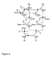
- Fig. 2 depicts a preferred embodiment of the differential amplifying circuit of the present invention where the total construction is low-pass.
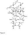
- Fig. 3 depicts the preferred embodiment of Fig. 1, with additional capacitor circuit elements.
- Fig. 4 shows a Spice simulation of the circuit of Figure 1 wherein the amplitude of the output voltage signal for a 1 mV stimulus on the inputs versus frequency for several Vbias voltages is detailed.
- Fig. 5 shows the common mode output voltage 30, and the voltages 31 on nodes 5 and 6 for Vbias between 0 and 3.3V of the circuit of Figure 1 (Spice simulation).
- a differential amplifying circuit having at least two branches wherein an output node is present, each of said branches comprising an amplifying element and a load element, said load element including a subcircuit for regulating the signal at the output node of the branch.
- the active loads in the two output branches of the differential amplifying circuit preferably an Operational Transconductance Amplifier (OTA), show a high conductance at low frequency and low conductance at higher frequency.
- the active loads in the two output branches of the OTA show high conductance at low frequency and low conductance at higher frequency.
- the frequency at which this conductance change happens is referred to as the low corner frequency of the pass band.
- the active loads in both parallel branches consist of a PMOS transistor (M3 & M4) connected as a current source, of which the gate is regulated by another PMOS transistor (M5 & M6) operating in triode region or in sub-threshold (see Figure 1).
- the common mode output voltage is determined by the PMOS-transistor parameters and the operating bias current.
- the regulation of the output common mode is in this way inherently present in the OTA circuit.
- the lower frequencies are only little amplified or even attenuated. This allows the input referred offset to be less deteriorating to the amplification process. This is because the input referred offset can be regarded as an addition to the input signal at DC-frequency.
- a first option is to place the two biasing transistors M5 & M6 in the sub-threshold regime. This keeps the layout area for the system limited.
- a leak 23, 24 may be organised to avoid start-up problems (see Figure 3).
- a second option is to add a capacitor 26 (also in figure 3).
- a third option is to add two capacitors 21, 22 of which each capacitor has one terminal fixed to the ground or to the Vcc power supply.
- the OTA is of the low-pass type, i.e. also amplifying DC signals. This is achieved by adding a wire between the gates of the aforementioned gates of current sources (M13, M14).
- M13, M14 current sources
- FIG. 1 A preferred embodiment of the present invention is shown in FIG. 1.
- a differential pair of NMOS transistors M1 and M2 is fed by a current source transistor M7 that mirrors the current Ibias injected in transistor M8. This is a typical way of driving a differential pair of transistors.
- Transistor M1 sees as active load the combination of transistors M5 and M3.
- M2 sees as active load M4 and M6.
- Transistors M3 and M4 operate as current source, whereby the current depends on the voltage on their gate nodes 5 and 6.
- Vbias is chosen such that transistors M5 and M6 operate in their triode region. Their functioning can then be summarised as a transistor that mimics a resistor.
- each of these resistors is then connected to the output node (node 3 for M5 and node 4 for M6), and the other side is connected to the gates of the current sources (transistor M3 and M4 respectively).
- These gates have a gate-channel capacitance.
- the resistance of M5 and M6 and the gate-channel capacitances of M3 and M4 form together two low pass filters.
- the voltage at nodes 5 and 6 follow the output nodes 3 and 4 respectively. In other words, the system operates as if nodes 3 and 5 are connected and 4 and 6 are connected.
- transistors M3 and M4 are configured as diodes, and the output nodes 3 and 4 have impedance essentially determined by transconductances g m3 and g m4 respectively.
- the amplification of the OTA at low frequency is then g m1 /g m3 .
- the biasing of a system is a DC question, and falls automatically into this frequency band.
- the nodes 5 and 6 will not follow the output signals, and the conductance of the output nodes becomes g 03 +g 01 and g 04 +g 02 respectively.
- the amplification of the OTA stage is then g m1 /(g 03 +g 01 ).
- Fig. 4 shows a Spice simulation for the structure in Fig. 1 with a Vcc of 3.3 V, and a Vbias of 600 mV. It illustrates the operation (see curve 600 mV).
- the low corner frequency of the pass band is about 100 kHz, below this frequency the amplifications is about 4.5, and above, the amplification is about 45.
- the high frequency cut-off is at about 100 MHz for this particular case.
- the low corner frequency is determined by the choice of the Vbias voltage.
- the Vbias voltage determines the effective resistance of the transistor M5 and M6, which subsequently determines the cut-off frequency of the internal low-pass filters. Resistors can as well replace transistor M5 and M6, if available in the used CMOS technology. Depending on the application, the value of the required resistors may be too large to remain implementable. Then the configuration with transistors M5 and M6 is an option.
- Figure 5 shows two voltages versus the applied Vbias. The voltage represented by curve 30 is the common mode output voltage, and curve 31 represents the voltage on nodes 5 and 6.
- Another way to lower the low corner frequency is to add elements to the basic circuit of fig. 1.
- the most effective is to add capacitance 26 (Fig. 3).
- the advantage of the latter solution is that of capacitances 21 and 22, one terminal (node 25) can be connected to Vcc or to ground.
- a capacitance can be made using e.g. a gate capacitance, or a semiconductor junction available in CMOS, e.g. from N-Well to substrate.
- Figure 2 shows an embodiment of the invention that is similar to the circuit of Fig. 1.
- the voltages on the two gates of M3 and M4 can change independently, whilst in Fig. 2, the gates of M13 and M14 are connected to each other (node 15).
- Vbias to a voltage, small enough such that M15 and M16 remain in the triode region, and large enough that the effective resistance M15 and 16 form do not become too small to weaken the amplification of the OTA.
- the main function of the circuit of Fig. 2 is a fully differential OTA, however not with a pass-band like the structure of Fig. 1.
- the curve indicated "connected 600mV" in Fig. 4 shows that there is no filtering at lower frequency.
Landscapes
- Engineering & Computer Science (AREA)
- Power Engineering (AREA)
- Amplifiers (AREA)
Priority Applications (3)
| Application Number | Priority Date | Filing Date | Title |
|---|---|---|---|
| EP99870162A EP1093221A1 (de) | 1999-07-19 | 1999-07-19 | Kompakter Transkonduktanz-Differenzverstärker und Verfahren zu seinem Betrieb |
| JP2000217571A JP2001068951A (ja) | 1999-07-19 | 2000-07-18 | 小型の相互コンダクタンス差動増幅器及びその駆動方法 |
| US09/619,753 US6426676B1 (en) | 1999-07-19 | 2000-07-19 | Compact differential transconductance amplifier and a method of operation thereof |
Applications Claiming Priority (1)
| Application Number | Priority Date | Filing Date | Title |
|---|---|---|---|
| EP99870162A EP1093221A1 (de) | 1999-07-19 | 1999-07-19 | Kompakter Transkonduktanz-Differenzverstärker und Verfahren zu seinem Betrieb |
Publications (1)
| Publication Number | Publication Date |
|---|---|
| EP1093221A1 true EP1093221A1 (de) | 2001-04-18 |
Family
ID=8243875
Family Applications (1)
| Application Number | Title | Priority Date | Filing Date |
|---|---|---|---|
| EP99870162A Withdrawn EP1093221A1 (de) | 1999-07-19 | 1999-07-19 | Kompakter Transkonduktanz-Differenzverstärker und Verfahren zu seinem Betrieb |
Country Status (3)
| Country | Link |
|---|---|
| US (1) | US6426676B1 (de) |
| EP (1) | EP1093221A1 (de) |
| JP (1) | JP2001068951A (de) |
Cited By (1)
| Publication number | Priority date | Publication date | Assignee | Title |
|---|---|---|---|---|
| WO2007102132A1 (en) * | 2006-03-09 | 2007-09-13 | Nxp B.V. | Amplification stage |
Families Citing this family (6)
| Publication number | Priority date | Publication date | Assignee | Title |
|---|---|---|---|---|
| JP4267983B2 (ja) * | 2002-09-25 | 2009-05-27 | 株式会社豊田中央研究所 | 起動信号出力回路 |
| US7138835B1 (en) | 2003-05-23 | 2006-11-21 | Xilinx, Inc. | Method and apparatus for an equalizing buffer |
| US8949083B2 (en) * | 2011-07-29 | 2015-02-03 | Globalfoundries Inc. | Modeling gate transconductance in a sub-circuit transistor model |
| CN105991099B (zh) * | 2015-01-30 | 2018-08-14 | 博通集成电路(上海)股份有限公司 | 运算放大器及使用该运算放大器进行放大的方法 |
| US11176888B2 (en) * | 2019-08-22 | 2021-11-16 | Apple Inc. | Auto-zero applied buffer for display circuitry |
| KR102772414B1 (ko) | 2019-10-07 | 2025-02-25 | 삼성전자주식회사 | 피드포워드 경로를 포함하는 완전 차동 증폭기 |
Citations (2)
| Publication number | Priority date | Publication date | Assignee | Title |
|---|---|---|---|---|
| US5469092A (en) * | 1993-09-13 | 1995-11-21 | Kabushiki Kaisha Toshiba | Electronic circuit including means for reflecting signal current and feed forward means for compensating operational speed thereof |
| US5736892A (en) * | 1993-12-10 | 1998-04-07 | Rambus, Inc. | Differential charge pump circuit with high differential impedance and low common mode impedance |
Family Cites Families (1)
| Publication number | Priority date | Publication date | Assignee | Title |
|---|---|---|---|---|
| NL8602894A (nl) * | 1986-11-14 | 1988-06-01 | Philips Nv | Filterschakeling. |
-
1999
- 1999-07-19 EP EP99870162A patent/EP1093221A1/de not_active Withdrawn
-
2000
- 2000-07-18 JP JP2000217571A patent/JP2001068951A/ja active Pending
- 2000-07-19 US US09/619,753 patent/US6426676B1/en not_active Expired - Fee Related
Patent Citations (2)
| Publication number | Priority date | Publication date | Assignee | Title |
|---|---|---|---|---|
| US5469092A (en) * | 1993-09-13 | 1995-11-21 | Kabushiki Kaisha Toshiba | Electronic circuit including means for reflecting signal current and feed forward means for compensating operational speed thereof |
| US5736892A (en) * | 1993-12-10 | 1998-04-07 | Rambus, Inc. | Differential charge pump circuit with high differential impedance and low common mode impedance |
Cited By (2)
| Publication number | Priority date | Publication date | Assignee | Title |
|---|---|---|---|---|
| WO2007102132A1 (en) * | 2006-03-09 | 2007-09-13 | Nxp B.V. | Amplification stage |
| CN101401300B (zh) * | 2006-03-09 | 2012-03-21 | Nxp股份有限公司 | 放大级 |
Also Published As
| Publication number | Publication date |
|---|---|
| US6426676B1 (en) | 2002-07-30 |
| JP2001068951A (ja) | 2001-03-16 |
Similar Documents
| Publication | Publication Date | Title |
|---|---|---|
| US4904952A (en) | Differential amplifier incorporating negative resistance | |
| US4554515A (en) | CMOS Operational amplifier | |
| JP2603968B2 (ja) | 線形差動増幅回路 | |
| US4213098A (en) | Semiconductor differential amplifier having feedback bias control for stabilization | |
| US4459555A (en) | MOS Differential amplifier gain control circuit | |
| US5345190A (en) | Modular low voltage filter with common mode feedback | |
| JP2003243938A (ja) | 半導体装置 | |
| US5099205A (en) | Balanced cascode current mirror | |
| US6680645B2 (en) | Active filter circuit with operational amplifier | |
| US6426676B1 (en) | Compact differential transconductance amplifier and a method of operation thereof | |
| US4912427A (en) | Power supply noise rejection technique for amplifiers | |
| US6642790B2 (en) | Differential, complementary amplifier | |
| US6043718A (en) | Temperature, supply and process-insensitive signal-controlled oscillators | |
| JP2599575B2 (ja) | 演算相互コンダクタンス増幅器 | |
| JPS60229513A (ja) | 同相モード二重帰還形の広帯城増幅器 | |
| JPH0235485B2 (de) | ||
| JPH10107559A (ja) | 低ノイズ増幅器構造体 | |
| US20050030092A1 (en) | Active filter circuit with operational amplifier | |
| EP0720078B1 (de) | Verfahren zur Spannungsschwelleextraktierung und Schaltung nach dem Verfahren | |
| DE69105905T2 (de) | Integrierte Verstärkerschaltung mit einziger Eingangssignalverbindung. | |
| US6873205B1 (en) | Active continuous-time filter with increased dynamic range in the presence of blocker signals | |
| US6556078B2 (en) | Integrated low-corner frequency high pass filter circuit | |
| US6031416A (en) | First and second order CMOS elementary cells for time-continuous analog filters | |
| KR100213240B1 (ko) | 이중 입력 연산 상호 콘덕턴스 증폭기를 이용한 필터 | |
| JP3858281B2 (ja) | サンプル/ホールド回路及びこれを用いた電荷転送装置、並びに電荷転送装置の駆動方法 |
Legal Events
| Date | Code | Title | Description |
|---|---|---|---|
| PUAI | Public reference made under article 153(3) epc to a published international application that has entered the european phase |
Free format text: ORIGINAL CODE: 0009012 |
|
| AK | Designated contracting states |
Kind code of ref document: A1 Designated state(s): AT BE CH CY DE DK ES FI FR GB GR IE IT LI LU MC NL PT SE |
|
| AX | Request for extension of the european patent |
Free format text: AL;LT;LV;MK;RO;SI |
|
| 17P | Request for examination filed |
Effective date: 20010621 |
|
| AKX | Designation fees paid |
Free format text: AT BE CH CY DE DK ES FI FR GB GR IE IT LI LU MC NL PT SE |
|
| STAA | Information on the status of an ep patent application or granted ep patent |
Free format text: STATUS: THE APPLICATION IS DEEMED TO BE WITHDRAWN |
|
| 18D | Application deemed to be withdrawn |
Effective date: 20060808 |