EP1094599B1 - Eine Schaltung zur Kompensation der Differenz der Vgs-Spannungen zweier MOS-Transistoren - Google Patents
Eine Schaltung zur Kompensation der Differenz der Vgs-Spannungen zweier MOS-Transistoren Download PDFInfo
- Publication number
- EP1094599B1 EP1094599B1 EP99830662A EP99830662A EP1094599B1 EP 1094599 B1 EP1094599 B1 EP 1094599B1 EP 99830662 A EP99830662 A EP 99830662A EP 99830662 A EP99830662 A EP 99830662A EP 1094599 B1 EP1094599 B1 EP 1094599B1
- Authority
- EP
- European Patent Office
- Prior art keywords
- mos transistor
- transistors
- transistor
- mirror
- current
- Prior art date
- Legal status (The legal status is an assumption and is not a legal conclusion. Google has not performed a legal analysis and makes no representation as to the accuracy of the status listed.)
- Expired - Lifetime
Links
- 238000010586 diagram Methods 0.000 description 3
- 230000005669 field effect Effects 0.000 description 2
- 238000004519 manufacturing process Methods 0.000 description 2
- 238000000034 method Methods 0.000 description 2
- 210000000746 body region Anatomy 0.000 description 1
- 230000000295 complement effect Effects 0.000 description 1
- 230000001419 dependent effect Effects 0.000 description 1
- 238000002347 injection Methods 0.000 description 1
- 239000007924 injection Substances 0.000 description 1
- 229910044991 metal oxide Inorganic materials 0.000 description 1
- 150000004706 metal oxides Chemical class 0.000 description 1
- 239000004065 semiconductor Substances 0.000 description 1
Images

Classifications
-
- H—ELECTRICITY
- H03—ELECTRONIC CIRCUITRY
- H03F—AMPLIFIERS
- H03F1/00—Details of amplifiers with only discharge tubes, only semiconductor devices or only unspecified devices as amplifying elements
- H03F1/30—Modifications of amplifiers to reduce influence of variations of temperature or supply voltage or other physical parameters
- H03F1/301—Modifications of amplifiers to reduce influence of variations of temperature or supply voltage or other physical parameters in MOSFET amplifiers
-
- H—ELECTRICITY
- H03—ELECTRONIC CIRCUITRY
- H03F—AMPLIFIERS
- H03F3/00—Amplifiers with only discharge tubes or only semiconductor devices as amplifying elements
- H03F3/30—Single-ended push-pull [SEPP] amplifiers; Phase-splitters therefor
- H03F3/3001—Single-ended push-pull [SEPP] amplifiers; Phase-splitters therefor with field-effect transistors
Definitions
- the present invention relates to a circuit for compensating for the difference between the gate-source voltages (Vgs) of two MOS transistors of a device in an integrated circuit as defined in the preamble of Claim 1.
- MOS transistors defines field-effect transistors which are produced by MOS (metal-oxide semiconductor) technology and are commonly used as basic components of devices in analog and digital integrated circuits.
- MOS metal-oxide semiconductor
- the invention also applies, in general, to circuits which use field-effect transistors of different types. This, is however not claimed.
- MOS transistors of different types or dimensions formed in the same circuit may respond differently to process variations. In many applications, particularly in analog circuits, this different behaviour of MOS transistors causes imbalances in the operation of the circuits or undesired deviations from the operation provided for at the design stage.
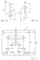
- a stage of this type comprises an n-channel transistor Mn and a p-channel transistor Mp having their source electrodes connected to the terminals of a supply, indicated by the ground symbol and VDD, and their gate electrodes connected to respective biasing circuits comprising, in this example, two identical current generators Go connected, as shown, to an input node N of the stage, each by means of a resistor Ro.
- the drain electrodes of the two transistors constitute two outputs of the stage and are connected to other components of the amplifier, not shown.
- the generators Go must generate identical currents
- the resistors Ro must have the same resistance
- the voltages Vgsn and Vgsp between the gates and sources of the two transistors Mn and Mp must be identical.
- the first two conditions can be satisfied by sufficient precision but the third cannot generally be satisfied because the two transistors are structurally different from one another and therefore have different characteristic curves. Moreover, the two transistors respond differently to temperature variations in operation.
- the object of the present invention is to propose a circuit which compensates for the difference owing to variations in the production process and/or to variations of other parameters, such as temperature, between the gate-source voltages of two MOS transistors of different types.
- Figure 2 shows schematically the amplifier stage of Figure 1, to which a circuit for compensating for the difference between the voltages Vgsn and Vgsp has been added.
- the compensation circuit represented by a block 10, generates a compensation current Io which is injected into the node N.
- the compensation circuit 10 comprises two MOS transistors, a p-channel transistor indicated Mp1, and an n-channel transistor indicated Mn1, which are of the same type as the transistors Mp and Mn of Figure 2, that is, which are manufactured in the same device and by the same process stages.
- the transistors Mp1 and Mn1 have the same dimensions as the transistors Mp and Mn, respectively but, in general, they could have different dimensions.
- Each of the two transistors Mp1 and Mn1 has its gate and drain electrodes connected to one another and the transistors Mp1 and Mn1 are connected between the supply terminals, each by means of a constant current generator.
- the constant current generators are constituted by two p-channel transistors Mp2 and Mp3 of which the source electrodes are connected together to the terminal VDD, the gate electrodes are connected together to a terminal VB2 of a constant voltage supply, one has its drain electrode connected to the source electrode of the transistor Mp1 at a node A1, and the other has its drain electrode connected to the drain electrode of the transistor Mn1 at a node A2.
- the transistor Mp1 has its body region connected to its source electrode.
- Each of the nodes A1 and A2 is connected to the input of a decoupling stage the outputs of which are connected to one another by means of a resistor R1.
- the decoupling stages are constituted by two p-channel MOS transistors Mp4 and Mp5 having their gate electrodes connected to the nodes A1 and A2, respectively, their source electrodes connected to the terminal VDD via respective constant current generators, and their drain electrodes connected to ground via the input branches of respective current mirrors Sp1 and Sp3.
- the constant-current generators are constituted, respectively, by two p-channel transistors Mp6 and Mp7 having their source electrodes connected together to the terminal VDD, their gate electrodes connected together to a terminal VB1 of a constant-voltage supply, and their drain electrodes connected to the source electrodes of the transistors Mp4 and Mp5, respectively.
- the output branches of the mirrors Sp1 and Sp3 are in series with the input and output branches, respectively, of a further current mirror Sp2, as shown in Figure 3.
- the circuit combination comprising the transistors Mp2 and Mp3 has the function of biasing the transistors Mp1 and Mn1
- the circuit combination comprising the decoupling stages Mp4 and Mp5 and the respective current generators Mp6 and Mp7 has the function of measuring the difference between the gate-source voltages Vgsp and Vgsn of the two transistors Mp1 and Mn1.
- the voltages of the nodes A1 and A2 relative to ground that is, the voltages Vgsp and Vgsn, are reproduced substantially unchanged, by means of the decoupling stages, at the terminals of the resistor R1, so that a current Id proportional to the difference between the voltages Vgsn and Vgsp flows through this resistor.
- Id (Vgsn-Vgsp)/R1 , where R1 is the resistance of the resistor R1, that the currents Ip4 and Ip5 passing through the transistors Mp4 and Mp5, respectively, differ from one another by 2Id, that the currents in the input and output branches of the mirror Sp2 are equal to Ip4, and that the current in the output branch of the mirror Sp3 is equal to Ip5.
- transistors Mp1 and Mn1 are not identical to the transistors Mp and Mn to be compensated but, for example, have different dimensions, it is necessary, in order to achieve the desired compensation, to select resistors Ro having resistances proportional to that of the resistor R1 with a proportionality factor dependent on the ratios between the dimensions of the transistors to be compensated and those of the transistors Mn1 and Mp1 of the compensation circuit 10, also taking account of the currents and the current ratios of the current mirrors.
- the transistors Mn' and Mp' may have their gate electrodes connected to their drain electrodes and may be biased by respective generators Gn and Gp connected between their drain electrodes and respective supply terminals Vdd and ground.
- the compensation current Io is injected into the drain electrode of the respective transistor Mn', Mp' via a resistor Ro'.
- the transistors Mn' and Mp' are identical to the transistors Mn1 and Mp1, respectively, compensation is achieved with the use of resistors Ro' having the same resistance as the resistor R1; otherwise, the resistance value is selected so as to be proportional to that of the resistor R1 with a proportionality factor which depends on the ratio between the dimensions of the transistors Mn' and Mp' to be compensated and those of the transistors Mn1 and Mp1 of the circuit 10.
- the compensated voltages Vn and Vp are given by the sum of the gate-source voltages Vgsn and Vgsp of the transistors Mn' and Mp', respectively, and by the voltage drop in the resistors Ro'.
- the mirrors Sp2 and Sp3 should have two separate output branches, as shown in Figure 5. Moreover, if there are more than two transistors to be compensated it may clearly be necessary to modify the mirrors Sp2 and Sp3 in a manner such that they have as many output branches as there are transistors to be compensated independently of one another.
Landscapes
- Engineering & Computer Science (AREA)
- Power Engineering (AREA)
- Amplifiers (AREA)
- Logic Circuits (AREA)
Claims (5)
- Eine Schaltung zum Kompensieren der Differenz zwischen den Gate-Source-Spannungen eines ersten MOS-Transistors (Mp) und eines zweiten MOS-Transistors (Mn) einer integrierten Schaltungsvorrichtung, dadurch gekennzeichnet, dass dieselbe folgende Merkmale aufweist:einen dritten MOS-Transistor (Mp1) und einen vierten MOS-Transistor (Mn1), die von dem gleichen Typ wie der erste Transistor (Mp) bzw. der zweite Transistor (Mn) sind und in der gleichen Vorrichtung gebildet sind,eine Einrichtung (VDD, Mp2, Mp3) zum Vorspannen des dritten Transistors (Mp1) und des vierten Transistors (Mn1),eine Einrichtung (Mp4 - Mp7) zum Messen der Differenz zwischen den Gate-Source-Spannungen des dritten und des vierten Transistors (Mp1, Mn1),eine Einrichtung (R1) zum Erzeugen eines Kompensationsstroms (Io), der eine vorbestimmte Funktion der gemessenen Differenz ist, undeine Einrichtung (S1 - Sp3, Ro) zum Modifizieren des Vorspannens des ersten MOS-Transistors (Mp) und des zweiten MOS-Transistors (Mn) mit der Verwendung des Kompensationsstroms (Io).
- Eine Schaltung gemäß Anspruch 1, bei der die Einrichtung zum Vorspannen des dritten Transistors (Mp1) und des vierten Transistors (Mn1) einen ersten Stromgenerator (Mp2) und einen zweiten Stromgenerator (Mp3) aufweist, die mit dem dritten MOS-Transistor (Mp1) bzw. mit dem vierten MOS-Transistor (Mn1) in Reihe geschaltet sind, und die Differenzmesseinrichtung eine erste Entkopplungsstufe (Mp4) und eine zweite Entkopplungsstufe (Mp5) aufweist, deren jeweilige Eingänge (A1, A2) zwischen die Source- und die Drain-Elektrode des dritten MOS-Transistors (Mp1) bzw. des vierten MOS-Transistors (Mn1) geschaltet sind und deren jeweilige Ausgänge mit der Einrichtung (R1) zum Erzeugen eines Kompensationsstroms (Io) verbunden sind.
- Eine Schaltung gemäß Anspruch 2, bei der die Einrichtung zum Modifizieren des Vorspannens einen ersten Stromspiegel (Sp1), einen zweiten Stromspiegel (Sp2) und einen dritten Stromspiegel (Sp3) und eine Einrichtung (Ro, Ro') zum Erzeugen einer Kompensationsspannung aufweist, wobei der erste Spiegel (Sp1) einen Eingangszweig, der mit einer (Mp4) der Entkopplungsstufen verbunden ist, und einen Ausgangszweig in Reihe mit einem Eingangszweig des zweiten Spiegels (Sp2) aufweist, wobei der dritte Spiegel (Sp3) einen Eingangszweig, der mit der anderen (Mp5) der Kopplungsstufen verbunden ist, und einen Ausgangszweig in Reihe mit einem Ausgangszweig des zweiten Spiegels (Sp2) aufweist, wobei die Einrichtung (Ro, Ro') zum Erzeugen einer Kompensationsspannung zwischen den Ausgangszweig des dritten Spiegels (Sp3) und eine vorbestimmte Elektrode von jedem des ersten und des zweiten MOS-Transistors (Mp, Mn) geschaltet ist.
- Eine Schaltung gemäß Anspruch 3, bei der der erste und der zweite MOS-Transistor ein p-Kanal-MOS-Transistor (Mp) und ein n-Kanal-MOS-Transistor (Mn) der Eingangsstufe eines Verstärkers sind, bei der der dritte und der vierte MOS-Transistor ein p-Kanal-MOS-Transistor (Mp1) und ein n-Kanal-MOS-Transistor (Mn1) sind, bei der die Einrichtung zum Erzeugen einer Kompensationsspannung zwei Widerstände (Ro) aufweist und bei der die vorbestimmte Elektrode die Gate-Elektrode ist.
- Eine Schaltung gemäß Anspruch 3, bei der der erste und der zweite MOS-Transistor ein p-Kanal-MOS-Transistor (Mp') und ein n-Kanal-MOS-Transistor (Mn') sind, deren Gate- und Drain-Elektroden jeweils miteinander verbunden sind, bei der die Einrichtung zum Erzeugen einer Kompensationsspannung zwei Widerstände (Ro') aufweist und bei der die vorbestimmte Elektrode die Drain-Elektrode ist.
Priority Applications (4)
| Application Number | Priority Date | Filing Date | Title |
|---|---|---|---|
| DE69922811T DE69922811D1 (de) | 1999-10-21 | 1999-10-21 | Eine Schaltung zur Kompensation der Differenz der Vgs-Spannungen zweier MOS-Transistoren |
| EP99830662A EP1094599B1 (de) | 1999-10-21 | 1999-10-21 | Eine Schaltung zur Kompensation der Differenz der Vgs-Spannungen zweier MOS-Transistoren |
| JP2000321411A JP3504919B2 (ja) | 1999-10-21 | 2000-10-20 | 2個のmosトランジスタのゲート・ソース電圧間の差を補償する回路 |
| US09/693,182 US6448839B1 (en) | 1999-10-21 | 2000-10-20 | Circuit for compensating for the difference between the Vgs voltages of two MOS transistors |
Applications Claiming Priority (2)
| Application Number | Priority Date | Filing Date | Title |
|---|---|---|---|
| EP99830662A EP1094599B1 (de) | 1999-10-21 | 1999-10-21 | Eine Schaltung zur Kompensation der Differenz der Vgs-Spannungen zweier MOS-Transistoren |
| US09/693,182 US6448839B1 (en) | 1999-10-21 | 2000-10-20 | Circuit for compensating for the difference between the Vgs voltages of two MOS transistors |
Publications (2)
| Publication Number | Publication Date |
|---|---|
| EP1094599A1 EP1094599A1 (de) | 2001-04-25 |
| EP1094599B1 true EP1094599B1 (de) | 2004-12-22 |
Family
ID=26153807
Family Applications (1)
| Application Number | Title | Priority Date | Filing Date |
|---|---|---|---|
| EP99830662A Expired - Lifetime EP1094599B1 (de) | 1999-10-21 | 1999-10-21 | Eine Schaltung zur Kompensation der Differenz der Vgs-Spannungen zweier MOS-Transistoren |
Country Status (3)
| Country | Link |
|---|---|
| US (1) | US6448839B1 (de) |
| EP (1) | EP1094599B1 (de) |
| JP (1) | JP3504919B2 (de) |
Families Citing this family (2)
| Publication number | Priority date | Publication date | Assignee | Title |
|---|---|---|---|---|
| US7512848B1 (en) * | 2004-09-29 | 2009-03-31 | Xilinx, Inc. | Clock and data recovery circuit having operating parameter compensation circuitry |
| FR3059492A1 (fr) * | 2016-11-29 | 2018-06-01 | Stmicroelectronics (Grenoble 2) Sas | Procede et dispositif d'amplification en mode commun autopolarise et autoregule. |
Citations (1)
| Publication number | Priority date | Publication date | Assignee | Title |
|---|---|---|---|---|
| US4442398A (en) * | 1980-11-14 | 1984-04-10 | Societe Pour L'etude Et La Fabrication De Circuits Integres Speciaux-E.F.C.I.S. | Integrated circuit generator in CMOS technology |
Family Cites Families (2)
| Publication number | Priority date | Publication date | Assignee | Title |
|---|---|---|---|---|
| JPS59196613A (ja) * | 1983-04-21 | 1984-11-08 | Toshiba Corp | 演算増幅回路 |
| DE4036115C2 (de) * | 1990-11-13 | 1997-12-11 | Max Planck Gesellschaft | Verfahren und Einrichtung zur quantitativen nichtresonanten Photoionisation von Neutralteilchen und Verwendung einer solchen Einrichtung |
-
1999
- 1999-10-21 EP EP99830662A patent/EP1094599B1/de not_active Expired - Lifetime
-
2000
- 2000-10-20 US US09/693,182 patent/US6448839B1/en not_active Expired - Lifetime
- 2000-10-20 JP JP2000321411A patent/JP3504919B2/ja not_active Expired - Fee Related
Patent Citations (1)
| Publication number | Priority date | Publication date | Assignee | Title |
|---|---|---|---|---|
| US4442398A (en) * | 1980-11-14 | 1984-04-10 | Societe Pour L'etude Et La Fabrication De Circuits Integres Speciaux-E.F.C.I.S. | Integrated circuit generator in CMOS technology |
Also Published As
| Publication number | Publication date |
|---|---|
| JP3504919B2 (ja) | 2004-03-08 |
| US6448839B1 (en) | 2002-09-10 |
| JP2001177349A (ja) | 2001-06-29 |
| EP1094599A1 (de) | 2001-04-25 |
Similar Documents
| Publication | Publication Date | Title |
|---|---|---|
| US5612614A (en) | Current mirror and self-starting reference current generator | |
| EP0194031B1 (de) | Bandlücken CMOS-Vergleichsspannungsschaltung | |
| JP4638481B2 (ja) | 差動段電圧オフセットトリム回路 | |
| KR101144024B1 (ko) | 전압 레벨 시프트 회로 및 반도체 집적 회로 | |
| EP0684698B1 (de) | Verstärkerausgangsstufe der Klasse "AB" | |
| KR100721736B1 (ko) | 정전류 회로 및 그 정전류 회로를 사용한 시스템 전원 장치 | |
| KR20000022517A (ko) | 정밀 밴드갭 기준 회로 | |
| US11181937B2 (en) | Correction current output circuit and reference voltage circuit with correction function | |
| US7317358B2 (en) | Differential amplifier circuit | |
| US7109697B1 (en) | Temperature-independent amplifier offset trim circuit | |
| KR101080560B1 (ko) | 트랜스컨덕턴스 조정 회로 | |
| US11112315B1 (en) | Blending temperature-dependent currents to generate bias current with temperature dependent profile | |
| CN100571025C (zh) | 差分级电压偏置微调电路 | |
| US5739682A (en) | Circuit and method for providing a reference circuit that is substantially independent of the threshold voltage of the transistor that provides the reference circuit | |
| US20180059707A1 (en) | Proportional to Absolute Temperature Reference Circuit and a Voltage Reference Circuit | |
| EP1094599B1 (de) | Eine Schaltung zur Kompensation der Differenz der Vgs-Spannungen zweier MOS-Transistoren | |
| US6175265B1 (en) | Current supply circuit and bias voltage circuit | |
| US5164614A (en) | Low power bias voltage generating circuit comprising a current mirror | |
| JP2021072033A (ja) | 電源回路 | |
| US5869957A (en) | Voltage divider circuit, differential amplifier circuit and semiconductor integrated circuit device | |
| KR100332508B1 (ko) | 안정화전류미러회로 | |
| US6081108A (en) | Level shifter/amplifier circuit | |
| KR20020047963A (ko) | 캐스코드 전류 미러의 전류 바이어스 회로 | |
| US5841311A (en) | Voltage subtracter circuit, voltage amplifier circuit, voltage divider circuit and semiconductor integrated circuit device | |
| KR19980070028A (ko) | 증폭기 및 반도체 집적 회로 장치 |
Legal Events
| Date | Code | Title | Description |
|---|---|---|---|
| PUAI | Public reference made under article 153(3) epc to a published international application that has entered the european phase |
Free format text: ORIGINAL CODE: 0009012 |
|
| AK | Designated contracting states |
Kind code of ref document: A1 Designated state(s): DE FR GB IT |
|
| AX | Request for extension of the european patent |
Free format text: AL;LT;LV;MK;RO;SI |
|
| 17P | Request for examination filed |
Effective date: 20011011 |
|
| AKX | Designation fees paid |
Free format text: DE FR GB IT |
|
| GRAP | Despatch of communication of intention to grant a patent |
Free format text: ORIGINAL CODE: EPIDOSNIGR1 |
|
| GRAS | Grant fee paid |
Free format text: ORIGINAL CODE: EPIDOSNIGR3 |
|
| GRAA | (expected) grant |
Free format text: ORIGINAL CODE: 0009210 |
|
| AK | Designated contracting states |
Kind code of ref document: B1 Designated state(s): DE FR GB IT |
|
| REG | Reference to a national code |
Ref country code: GB Ref legal event code: FG4D |
|
| REF | Corresponds to: |
Ref document number: 69922811 Country of ref document: DE Date of ref document: 20050127 Kind code of ref document: P |
|
| PG25 | Lapsed in a contracting state [announced via postgrant information from national office to epo] |
Ref country code: DE Free format text: LAPSE BECAUSE OF FAILURE TO SUBMIT A TRANSLATION OF THE DESCRIPTION OR TO PAY THE FEE WITHIN THE PRESCRIBED TIME-LIMIT Effective date: 20050323 |
|
| ET | Fr: translation filed | ||
| PLBE | No opposition filed within time limit |
Free format text: ORIGINAL CODE: 0009261 |
|
| STAA | Information on the status of an ep patent application or granted ep patent |
Free format text: STATUS: NO OPPOSITION FILED WITHIN TIME LIMIT |
|
| 26N | No opposition filed |
Effective date: 20050923 |
|
| PGFP | Annual fee paid to national office [announced via postgrant information from national office to epo] |
Ref country code: IT Payment date: 20071018 Year of fee payment: 9 |
|
| PGFP | Annual fee paid to national office [announced via postgrant information from national office to epo] |
Ref country code: FR Payment date: 20071030 Year of fee payment: 9 |
|
| REG | Reference to a national code |
Ref country code: FR Ref legal event code: ST Effective date: 20090630 |
|
| PG25 | Lapsed in a contracting state [announced via postgrant information from national office to epo] |
Ref country code: IT Free format text: LAPSE BECAUSE OF NON-PAYMENT OF DUE FEES Effective date: 20081021 |
|
| PG25 | Lapsed in a contracting state [announced via postgrant information from national office to epo] |
Ref country code: FR Free format text: LAPSE BECAUSE OF NON-PAYMENT OF DUE FEES Effective date: 20081031 |
|
| PGFP | Annual fee paid to national office [announced via postgrant information from national office to epo] |
Ref country code: GB Payment date: 20110926 Year of fee payment: 13 |
|
| GBPC | Gb: european patent ceased through non-payment of renewal fee |
Effective date: 20121021 |
|
| PG25 | Lapsed in a contracting state [announced via postgrant information from national office to epo] |
Ref country code: GB Free format text: LAPSE BECAUSE OF NON-PAYMENT OF DUE FEES Effective date: 20121021 |