EP1096294A2 - Elément optique pour contrôler la séparation de faisceaux multiples - Google Patents
Elément optique pour contrôler la séparation de faisceaux multiples Download PDFInfo
- Publication number
- EP1096294A2 EP1096294A2 EP00123261A EP00123261A EP1096294A2 EP 1096294 A2 EP1096294 A2 EP 1096294A2 EP 00123261 A EP00123261 A EP 00123261A EP 00123261 A EP00123261 A EP 00123261A EP 1096294 A2 EP1096294 A2 EP 1096294A2
- Authority
- EP
- European Patent Office
- Prior art keywords
- light beam
- optical element
- exit surface
- incident surface
- optical axis
- Prior art date
- Legal status (The legal status is an assumption and is not a legal conclusion. Google has not performed a legal analysis and makes no representation as to the accuracy of the status listed.)
- Granted
Links
Images

Classifications
-
- G—PHYSICS
- G02—OPTICS
- G02B—OPTICAL ELEMENTS, SYSTEMS OR APPARATUS
- G02B27/00—Optical systems or apparatus not provided for by any of the groups G02B1/00 - G02B26/00, G02B30/00
- G02B27/10—Beam splitting or combining systems
- G02B27/12—Beam splitting or combining systems operating by refraction only
- G02B27/126—The splitting element being a prism or prismatic array, including systems based on total internal reflection
Definitions
- the present invention relates to multiple beam separation control and, more particularly, to a refractive optical element, which controls separation of two closely spaced laser beams.
- High speed or color printing requires a multiple beam light source.
- One possible multiple beam light source is a laser diode array which is currently expensive and difficult to fabricate.
- Another approach to providing a multiple beam light source is to integrate individual laser diodes to form the multiple light beam source.
- the major problem with integrating individual laser diodes into a multiple beam light source is the large spacing between the individual laser diodes.
- the spacing or pitch between two adjacent individual laser diodes can be 100 microns or larger while the required spacing of the two adjacent light beams for printing uses is 25 microns or less, a difference of a factor of four or greater.
- Beam separation control uses optical elements to contract the pitch or spacing between light beams.
- Beam combiners are optical elements that combine two or more light beams into a single overlapping composite beam.
- Beam combiners can be refractive optical elements such as prisms, diffractive optical elements such as diffraction gratings and reflective optical elements such as dichroic or partially silvered mirrors. Beam combiners are distinctly different optical elements from beam separation control.
- Beam splitter prisms can be used for beam separation control but this approach reduces the intensity of the output beam by half due to light loss caused by splitting the beam.
- a refractive optical element provides beam separation control for two or four light beams by refracting each beam from an incident surface through the optical element to be refracted from a parallel exit surface out of the optical element.
- the beams have closer beam to beam spacing after the refraction from the optical element than before.
- the incident and exit surfaces are angled relative to and symmetric around an optical axis.
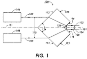
- the single refractive optical element 100 of the present invention provides beam separation control for the dual light beams 102 and 104 emitted by the two individual laser diodes 106 and 108.
- the two light beams 102 and 104 are symmetric around the optical axis 101 and equally spaced from the optical axis 101 in the direction of light propagation.
- the single refractive optical element 100 is symmetric around the optical axis 101 in the direction of light propagation.
- the first laser diode 106 emits the first light beam 102.
- the first light beam 102 is diverging and of a single wavelength.
- the second laser diode 108 emits the second light beam 104.
- the second light beam 104 is diverging and has the same single wavelength as the first light beam 102.
- the two individual laser diodes 106 and 108 are not part of an array but can share a common assembly.
- the dual light beams 102 and 104 are parallel to each other and separated by a first beam to beam spacing distance 110 of 100 microns.
- beam to beam spacing distances are measure from the center of the first beam to the center of the second beam.
- the optical element 100 is a single solid element formed of a material that transmits light of the wavelength of light beams 102 and 104 and has a uniform index of refraction throughout the material. Examples would include plastics and BK7 glass, as are known in the art.
- the optical element 100 has six flat facet surfaces and has a diamond pattern with a right triangle concave insert on the back corner.
- the optical element has a first incident surface 112 adjacent to a second incident surface 114.
- the optical element has a first exit surface 116 adjacent to a second exit surface 118.
- the optical element has a fifth surface 120, which is adjacent to the first incident surface 112 and the first exit surface 116.
- the optical element has a sixth surface 122, which is adjacent to the second incident surface 114 and the second exit surface 118.
- the first incident surface 112 is at a specified angle 124 with the second incident surface 114 and symmetric around the optical axis 101.
- the first exit surface 116 is at the same specified angle 126 with the second exit surface 118 and symmetric around the optical axis 101.
- the first incident surface 112 is parallel to the first exit surface 116.
- the second incident surface 114 is parallel to the second exit surface 116.
- angles 124 and 126 are right angles, as are all the other angles between the surfaces.
- the surfaces are angled relative to the optical axis.
- these angles 124 and 126 need not be right angles.
- the key features of this invention are the first incident surface and the first exit surface being parallel, the second incident surface and the second exit surface being parallel, the first and second incident surfaces being symmetrical around and angled relative to the optical axis and the first and second exit surfaces being symmetrical around and angled relative to the optical axis.
- the first light beam 102 will be incident upon the first incident surface 112.
- the light beam 102 will be refracted by the surface 112 and transmitted through the optical element 100 to the first exit surface 114.
- the first light beam 102 will be refracted by the first exit surface 114 to emerge out of the optical element 100.
- the first incident surface 112 is parallel to the first exit surface 116, the first light beam 102 exiting the optical element 100 will be parallel and collinear but positionally displaced to the first light beam 102 entering the optical element. Positionally displacement is measured in the beam to beam spacing relative to the optical axis.
- the second light beam 104 will be incident upon the second incident surface 114.
- the light beam 104 will be refracted by the surface 114 and transmitted through the optical element 100 to the second exit surface 116.
- the second light beam 104 will be refracted by the second exit surface 116 to emerge out of the optical element 100.
- the second incident surface 114 is parallel to the second exit surface 118, the second light beam 104 exiting the optical element 100 will be parallel and collinear but positionally displaced to the second light beam 104 entering the optical element.
- the first light beam 102 and the second light beam 104 will be refracted from the optical element 100 parallel to each other and separated by a second beam to beam spacing distance 128 of 25 microns.
- the second spacing distance 128 of 25 microns after the beams 102 and 104 have been through the optical element 100 is smaller than the first spacing distance 110 of 100 microns before the beams 102 and 104 have been through the optical element 100. While retaining the parallelism of the two beams, the optical element has provided beam separation control by spacing the two beams closer together.
- the distance of displacement of the beam through the optical element will equal the thickness of the optical element times the sine of the angle of incidence of the beam to the incident surface times a first fraction with a numerator of 1 minus the cosine of the angle of incidence and a denominator of the square root of a second fraction with a numerator of the index of refraction of the material of the optical element and a denominator of the index of refraction of atmosphere, that second fraction minus the sine squared of the angle of incidence.
- the optical element 100 of Figure 1 has six flat facet surfaces and has a diamond pattern with a right triangle concave insert on the back corner.
- the optical element could alternately have a flat front surface between the first and second incident surfaces or a flat back surface between the first and second exit surfaces.
- the first and second exit surfaces could be the same length as the first and second incident surfaces providing a chevron shape to the optical element.
- the only requirement for the shape of the optical element is the first incident surface and the first exit surface being parallel, the second incident surface and the second exit surface being parallel, the first and second incident surfaces being symmetrical around and angled relative to the optical axis and the first and second exit surfaces being symmetrical around and angled relative to the optical axis.
- the single refractive optical element 200 of the present invention provides beam separation control for the four light beams 202, 204, 206 and 208 emitted by the four individual laser diodes 210, 212, 214, and 216.
- the second and third light beams 204 and 206 are symmetric around the optical axis 201 and equally spaced from the optical axis 201 in the direction of light propagation.
- the first and fourth light beams 202 and 208 are symmetric around the optical axis 201 and equally spaced from the optical axis 201 in the direction of light propagation.
- the single refractive optical element 200 is symmetric around the optical axis 201 in the direction of light propagation.
- the first laser diode 210 emits the first light beam 202.
- the second laser diode 212 emits the second light beam 204.
- the third laser diode 214 emits the third light beam 206.
- the fourth laser diode 216 emits the fourth light beam 208. All four light beams 202, 204, 206 and 208 are diverging and have the same single wavelength.
- the four individual laser diodes 210, 212, 214, and 216 are not part of an array but can share a common assembly.
- the second and third incident surfaces 220 and 222 are at a first specified angle with each other and symmetric around the optical axis 201 and equally spaced from the optical axis 201 in the direction of light propagation.
- the first and fourth incident surfaces 218 and 224 are at a second specified angle from each other and symmetric around the optical axis 201 and equally spaced from the optical axis 201 in the direction of light propagation.
- the second and third exit surfaces 228 and 230 are at the first specified angle with each other and symmetric around the optical axis 201 and equally spaced from the optical axis 201 in the direction of light propagation.
- the first and fourth exit surfaces 226 and 232 are at the second specified angle from each other and symmetric around the optical axis 201 and equally spaced from the optical axis 201 in the direction of light propagation.
- the first incident surface 218 is parallel to the first exit surface 226.
- the second incident surface 220 is parallel to the second exit surface 228.
- the third incident surface 222 is parallel to the third exit surface 230.
- the fourth incident surface 224 is parallel to the fourth exit surface 232.
- the first light beam 202 will be incident upon the first incident surface 218.
- the light beam 202 will be refracted by the surface 218 and transmitted through the optical element 200 to the first exit surface 226.
- the first light beam 202 will be refracted by the first exit surface 226 to emerge out of the optical element 200.
- the first incident surface 218 is parallel to the first exit surface 226, the first light beam 202 exiting the optical element 200 will be parallel and collinear but positionally displaced to the first light beam 202 entering the optical element.
- the second light beam 204 will be incident upon the second incident surface 220.
- the light beam 204 will be refracted by the surface 220 and transmitted through the optical element 200 to the second exit surface 228.
- the second light beam 204 will be refracted by the second exit surface 228 to emerge out of the optical element 200.
- the second incident surface 220 is parallel to the second exit surface 228, the second light beam 204 exiting the optical element 200 will be parallel and collinear but positionally displaced to the second light beam 204 entering the optical element.
- the third light beam 206 will be incident upon the third incident surface 222.
- the light beam 206 will be refracted by the surface 222 and transmitted through the optical element 200 to the third exit surface 230.
- the third light beam 206 will be refracted by the third exit surface 230 to emerge out of the optical element 200.
- the third incident surface 222 is parallel to the third exit surface 230, the third light beam 206 exiting the optical element 200 will be parallel and collinear but positionally displaced to the third light beam 206 entering the optical element.
- the fourth light beam 208 will be incident upon the fourth incident surface 224.
- the light beam 208 will be refracted by the surface 224 and transmitted through the optical element 200 to the fourth exit surface 232.
- the fourth light beam 208 will be refracted by the fourth exit surface 232 to emerge out of the optical element 200.
- the fourth incident surface 224 is parallel to the fourth exit surface 232, the fourth light beam 208 exiting the optical element 200 will be parallel and collinear but positionally displaced to the fourth light beam 208 entering the optical element.
- the second and third light beams 204 and 206 are separated by a first beam to beam spacing distance 234 before the optical element 200.
- the second and third light beams 204 and 206 will be refracted from the optical element 200 parallel to each other and separated by a second beam to beam spacing distance 236.
- the second spacing distance 236 is smaller than the first spacing distance 234. While retaining the parallelism of the two beams, the optical element has provided beam separation control by spacing the two beams closer together.
- the first and fourth light beams 202 and 208 are separated by a third beam to beam spacing distance 238 before the optical element 200.
- the first and fourth light beams 202 and 208 will be refracted from the optical element 200 parallel to each other and separated by a fourth beam to beam spacing distance 240.
- the fourth spacing distance 240 is smaller than the third spacing distance 238. While retaining the parallelism of the two beams, the optical element has provided beam separation control by spacing the two beams closer together.
- the optical element 200 can provide beam separation control for less than four beams with two or three beams being incident on adjacent incident surfaces.
- Each beam can be individually modulated with either optical element 100 or 200.
Landscapes
- Physics & Mathematics (AREA)
- General Physics & Mathematics (AREA)
- Optics & Photonics (AREA)
- Optical Elements Other Than Lenses (AREA)
- Lenses (AREA)
- Semiconductor Lasers (AREA)
Applications Claiming Priority (2)
| Application Number | Priority Date | Filing Date | Title |
|---|---|---|---|
| US428390 | 1989-10-27 | ||
| US09/428,390 US6301054B1 (en) | 1999-10-28 | 1999-10-28 | Optical element for multiple beam separation control |
Publications (3)
| Publication Number | Publication Date |
|---|---|
| EP1096294A2 true EP1096294A2 (fr) | 2001-05-02 |
| EP1096294A3 EP1096294A3 (fr) | 2003-12-10 |
| EP1096294B1 EP1096294B1 (fr) | 2006-03-22 |
Family
ID=23698706
Family Applications (1)
| Application Number | Title | Priority Date | Filing Date |
|---|---|---|---|
| EP00123261A Expired - Lifetime EP1096294B1 (fr) | 1999-10-28 | 2000-10-26 | Elément optique pour contrôler la séparation de faisceaux multiples |
Country Status (3)
| Country | Link |
|---|---|
| US (1) | US6301054B1 (fr) |
| EP (1) | EP1096294B1 (fr) |
| DE (1) | DE60026771T2 (fr) |
Cited By (3)
| Publication number | Priority date | Publication date | Assignee | Title |
|---|---|---|---|---|
| WO2013167824A1 (fr) * | 2012-05-09 | 2013-11-14 | Archimej Technology | Dispositif d'emission d'un faisceau lumineux de spectre controle |
| FR2990582A1 (fr) * | 2012-11-20 | 2013-11-15 | Archimej Technology | Dispositif d'emission d'un faisceau lumineux de spectre controle. |
| FR2990512A1 (fr) * | 2012-05-09 | 2013-11-15 | Mejdi Nciri | Spectrometre d'absorption |
Families Citing this family (9)
| Publication number | Priority date | Publication date | Assignee | Title |
|---|---|---|---|---|
| DE19939750C2 (de) * | 1999-08-21 | 2001-08-23 | Laserline Ges Fuer Entwicklung | Optische Anordnung zur Verwendung bei einer Laserdiodenanordnung sowie Laserdiodenanordnung mit einer solchen optischen Anordnung |
| US6400512B1 (en) * | 2000-11-28 | 2002-06-04 | Xerox Corporation | Refractive/reflective optical element multiple beam spacer |
| CN2453457Y (zh) * | 2000-12-14 | 2001-10-10 | 福建华科光电有限公司 | 一种阵列型光学结构 |
| US6600605B1 (en) * | 2001-09-28 | 2003-07-29 | Spectra-Physics Semiconductor Lasers, Inc. | Diode beam transformation |
| US6987240B2 (en) * | 2002-04-18 | 2006-01-17 | Applied Materials, Inc. | Thermal flux processing by scanning |
| CA2458123C (fr) * | 2003-03-13 | 2012-05-15 | New Era Technology, Inc. | Teledetection des fuites de gaz |
| JP5141080B2 (ja) * | 2007-04-10 | 2013-02-13 | セイコーエプソン株式会社 | 光源装置、及び、それを用いた画像表示装置、モニタ装置、並びに照明装置 |
| CN114309923A (zh) * | 2021-12-17 | 2022-04-12 | 深圳市大族数控科技股份有限公司 | 光束间距调节模组及加工设备 |
| CN120762002A (zh) * | 2024-03-29 | 2025-10-10 | 深圳引望智能技术有限公司 | 一种发射系统、雷达及终端 |
Family Cites Families (7)
| Publication number | Priority date | Publication date | Assignee | Title |
|---|---|---|---|---|
| US5155628A (en) * | 1988-11-04 | 1992-10-13 | Dosmann Andrew J | Optical transmission spectrometer |
| JPH02246030A (ja) * | 1989-03-17 | 1990-10-01 | Ricoh Co Ltd | 光情報記録再生装置 |
| JPH05257081A (ja) * | 1992-02-05 | 1993-10-08 | Nec Corp | 光送信機 |
| US5566024A (en) | 1993-12-23 | 1996-10-15 | Xerox Corporation | Beam separation control and beam splitting by single blazed binary diffraction optical element |
| US5548444A (en) * | 1994-07-06 | 1996-08-20 | Hughes Danbury Optical Systems, Inc. | Optical beam homogenizing apparatus and method |
| IL115864A (en) * | 1995-11-02 | 1999-05-09 | Orbotech Ltd | Method and apparatus for delivering laser energy to an object |
| US5986794A (en) * | 1997-02-01 | 1999-11-16 | Laserline Gesellschaft Fur Entwicklung Und Vertrieb Von Diodenlasern Mbh | Laser optics and diode laser |
-
1999
- 1999-10-28 US US09/428,390 patent/US6301054B1/en not_active Expired - Lifetime
-
2000
- 2000-10-26 EP EP00123261A patent/EP1096294B1/fr not_active Expired - Lifetime
- 2000-10-26 DE DE60026771T patent/DE60026771T2/de not_active Expired - Lifetime
Cited By (6)
| Publication number | Priority date | Publication date | Assignee | Title |
|---|---|---|---|---|
| WO2013167824A1 (fr) * | 2012-05-09 | 2013-11-14 | Archimej Technology | Dispositif d'emission d'un faisceau lumineux de spectre controle |
| FR2990524A1 (fr) * | 2012-05-09 | 2013-11-15 | Archimej Technology | Dispositif d'emission d'un faisceau lumineux de spectre controle. |
| FR2990512A1 (fr) * | 2012-05-09 | 2013-11-15 | Mejdi Nciri | Spectrometre d'absorption |
| CN104380065A (zh) * | 2012-05-09 | 2015-02-25 | 阿奇麦杰科技公司 | 用于发射受控光谱的光束的发射装置 |
| CN104380065B (zh) * | 2012-05-09 | 2016-12-28 | 阿奇麦杰科技公司 | 用于发射受控光谱的光束的发射装置 |
| FR2990582A1 (fr) * | 2012-11-20 | 2013-11-15 | Archimej Technology | Dispositif d'emission d'un faisceau lumineux de spectre controle. |
Also Published As
| Publication number | Publication date |
|---|---|
| EP1096294B1 (fr) | 2006-03-22 |
| DE60026771T2 (de) | 2006-09-07 |
| EP1096294A3 (fr) | 2003-12-10 |
| DE60026771D1 (de) | 2006-05-11 |
| US6301054B1 (en) | 2001-10-09 |
Similar Documents
| Publication | Publication Date | Title |
|---|---|---|
| US4748614A (en) | Optical wavelength-multiplexing and/or demultiplexing device | |
| US4643519A (en) | Wavelength division optical multiplexer/demultiplexer | |
| US5457573A (en) | Diffraction element and an optical multiplexing/demultiplexing device incorporating the same | |
| US6301054B1 (en) | Optical element for multiple beam separation control | |
| US6239891B1 (en) | Optical demultiplexer and method of assembling same | |
| US4707056A (en) | Optical arrangement having a concave mirror or concave grating | |
| JP2000137139A (ja) | 光学的光束変換装置 | |
| US7199926B2 (en) | Diffraction grating device and optical apparatus | |
| CA1280921C (fr) | Multiplexeur-demultiplexeur optique | |
| JPH0693044B2 (ja) | プリズム光学系及びそれを用いた情報装置 | |
| JP2003506738A (ja) | 回折光学レンズを使用した波長分割多重化装置/デマルチプレキシング装置 | |
| JP2995985B2 (ja) | 偏光解消板 | |
| US6400512B1 (en) | Refractive/reflective optical element multiple beam spacer | |
| US6469831B2 (en) | Multibeam optical system | |
| US6810170B2 (en) | Optical signal processor | |
| US6768838B2 (en) | Optical module | |
| JPH0814647B2 (ja) | 光分波器 | |
| JP3412706B2 (ja) | 光合分波装置 | |
| JP2004061727A (ja) | 光源用モジュールおよび光源装置 | |
| US20020024733A1 (en) | Achromatic beam shaping prism | |
| US6407867B1 (en) | Multiple beam spacer with a beam splitter cube and two roof mirrors | |
| US6381073B1 (en) | Single refractive element and segmented mirror multiple beam spacer | |
| JP4138321B2 (ja) | 光分離方法および光合成方法および光分離合成光学素子および光分離カップリング装置 | |
| JPS63121813A (ja) | レ−ザ−切断用光学系 | |
| CN220440117U (zh) | 一种多光束激光发生器 |
Legal Events
| Date | Code | Title | Description |
|---|---|---|---|
| PUAI | Public reference made under article 153(3) epc to a published international application that has entered the european phase |
Free format text: ORIGINAL CODE: 0009012 |
|
| AK | Designated contracting states |
Kind code of ref document: A2 Designated state(s): AT BE CH CY DE DK ES FI FR GB GR IE IT LI LU MC NL PT SE |
|
| AX | Request for extension of the european patent |
Free format text: AL;LT;LV;MK;RO;SI |
|
| PUAL | Search report despatched |
Free format text: ORIGINAL CODE: 0009013 |
|
| AK | Designated contracting states |
Kind code of ref document: A3 Designated state(s): AT BE CH CY DE DK ES FI FR GB GR IE IT LI LU MC NL PT SE |
|
| AX | Request for extension of the european patent |
Extension state: AL LT LV MK RO SI |
|
| 17P | Request for examination filed |
Effective date: 20040611 |
|
| AKX | Designation fees paid |
Designated state(s): DE FR GB |
|
| 17Q | First examination report despatched |
Effective date: 20040805 |
|
| GRAP | Despatch of communication of intention to grant a patent |
Free format text: ORIGINAL CODE: EPIDOSNIGR1 |
|
| GRAS | Grant fee paid |
Free format text: ORIGINAL CODE: EPIDOSNIGR3 |
|
| GRAA | (expected) grant |
Free format text: ORIGINAL CODE: 0009210 |
|
| AK | Designated contracting states |
Kind code of ref document: B1 Designated state(s): DE FR GB |
|
| REG | Reference to a national code |
Ref country code: GB Ref legal event code: FG4D |
|
| REF | Corresponds to: |
Ref document number: 60026771 Country of ref document: DE Date of ref document: 20060511 Kind code of ref document: P |
|
| ET | Fr: translation filed | ||
| PLBE | No opposition filed within time limit |
Free format text: ORIGINAL CODE: 0009261 |
|
| STAA | Information on the status of an ep patent application or granted ep patent |
Free format text: STATUS: NO OPPOSITION FILED WITHIN TIME LIMIT |
|
| 26N | No opposition filed |
Effective date: 20061227 |
|
| REG | Reference to a national code |
Ref country code: FR Ref legal event code: PLFP Year of fee payment: 17 |
|
| PGFP | Annual fee paid to national office [announced via postgrant information from national office to epo] |
Ref country code: GB Payment date: 20160928 Year of fee payment: 17 |
|
| PGFP | Annual fee paid to national office [announced via postgrant information from national office to epo] |
Ref country code: FR Payment date: 20160921 Year of fee payment: 17 |
|
| PGFP | Annual fee paid to national office [announced via postgrant information from national office to epo] |
Ref country code: DE Payment date: 20160922 Year of fee payment: 17 |
|
| REG | Reference to a national code |
Ref country code: DE Ref legal event code: R119 Ref document number: 60026771 Country of ref document: DE |
|
| GBPC | Gb: european patent ceased through non-payment of renewal fee |
Effective date: 20171026 |
|
| REG | Reference to a national code |
Ref country code: FR Ref legal event code: ST Effective date: 20180629 |
|
| PG25 | Lapsed in a contracting state [announced via postgrant information from national office to epo] |
Ref country code: GB Free format text: LAPSE BECAUSE OF NON-PAYMENT OF DUE FEES Effective date: 20171026 Ref country code: DE Free format text: LAPSE BECAUSE OF NON-PAYMENT OF DUE FEES Effective date: 20180501 |
|
| PG25 | Lapsed in a contracting state [announced via postgrant information from national office to epo] |
Ref country code: FR Free format text: LAPSE BECAUSE OF NON-PAYMENT OF DUE FEES Effective date: 20171031 |