EP1096845A1 - Transparentes Material zur Abschirmung gegen elektromagnetische Strahlung und dessen Herstellungsverfahren - Google Patents
Transparentes Material zur Abschirmung gegen elektromagnetische Strahlung und dessen Herstellungsverfahren Download PDFInfo
- Publication number
- EP1096845A1 EP1096845A1 EP00308811A EP00308811A EP1096845A1 EP 1096845 A1 EP1096845 A1 EP 1096845A1 EP 00308811 A EP00308811 A EP 00308811A EP 00308811 A EP00308811 A EP 00308811A EP 1096845 A1 EP1096845 A1 EP 1096845A1
- Authority
- EP
- European Patent Office
- Prior art keywords
- layer
- metallic
- black
- transparent
- electromagnetic radiation
- Prior art date
- Legal status (The legal status is an assumption and is not a legal conclusion. Google has not performed a legal analysis and makes no representation as to the accuracy of the status listed.)
- Withdrawn
Links
Images

Classifications
-
- H—ELECTRICITY
- H05—ELECTRIC TECHNIQUES NOT OTHERWISE PROVIDED FOR
- H05K—PRINTED CIRCUITS; CASINGS OR CONSTRUCTIONAL DETAILS OF ELECTRIC APPARATUS; MANUFACTURE OF ASSEMBLAGES OF ELECTRICAL COMPONENTS
- H05K9/00—Screening of apparatus or components against electric or magnetic fields
- H05K9/0073—Shielding materials
- H05K9/0094—Shielding materials being light-transmitting, e.g. transparent, translucent
- H05K9/0096—Shielding materials being light-transmitting, e.g. transparent, translucent for television displays, e.g. plasma display panel
-
- H—ELECTRICITY
- H01—ELECTRIC ELEMENTS
- H01J—ELECTRIC DISCHARGE TUBES OR DISCHARGE LAMPS
- H01J29/00—Details of cathode-ray tubes or of electron-beam tubes of the types covered by group H01J31/00
- H01J29/86—Vessels; Containers; Vacuum locks
- H01J29/867—Means associated with the outside of the vessel for shielding, e.g. magnetic shields
- H01J29/868—Screens covering the input or output face of the vessel, e.g. transparent anti-static coatings, X-ray absorbing layers
-
- H—ELECTRICITY
- H01—ELECTRIC ELEMENTS
- H01J—ELECTRIC DISCHARGE TUBES OR DISCHARGE LAMPS
- H01J9/00—Apparatus or processes specially adapted for the manufacture, installation, removal, maintenance of electric discharge tubes, discharge lamps, or parts thereof; Recovery of material from discharge tubes or lamps
- H01J9/20—Manufacture of screens on or from which an image or pattern is formed, picked up, converted or stored; Applying coatings to the vessel
-
- H—ELECTRICITY
- H01—ELECTRIC ELEMENTS
- H01J—ELECTRIC DISCHARGE TUBES OR DISCHARGE LAMPS
- H01J2211/00—Plasma display panels with alternate current induction of the discharge, e.g. AC-PDPs
- H01J2211/20—Constructional details
- H01J2211/34—Vessels, containers or parts thereof, e.g. substrates
- H01J2211/44—Optical arrangements or shielding arrangements, e.g. filters or lenses
- H01J2211/446—Electromagnetic shielding means; Antistatic means
-
- H—ELECTRICITY
- H01—ELECTRIC ELEMENTS
- H01J—ELECTRIC DISCHARGE TUBES OR DISCHARGE LAMPS
- H01J2229/00—Details of cathode ray tubes or electron beam tubes
- H01J2229/0007—Elimination of unwanted or stray electromagnetic effects
- H01J2229/0015—Preventing or cancelling fields leaving the enclosure
- H01J2229/0023—Passive means
-
- H—ELECTRICITY
- H01—ELECTRIC ELEMENTS
- H01J—ELECTRIC DISCHARGE TUBES OR DISCHARGE LAMPS
- H01J2229/00—Details of cathode ray tubes or electron beam tubes
- H01J2229/863—Passive shielding means associated with the vessel
- H01J2229/8636—Electromagnetic shielding
Definitions
- This invention relates to a transparent electromagnetic radiation shield material for placement in front of a display device or the like to block electromagnetic radiation, and to a method of producing the material.
- the transparent electromagnetic radiation shield material is particularly suitable for a panel for a large plasma display.
- An electromagnetic radiation shield material for placement in front of a display device or the like is required to have not only excellent electromagnetic radiation shielding capability but also excellent transparency (optical transmittance), good clarity (degree of coating blackness etc.), wide viewing angle and the like.
- Japanese Patent Application Laid-Open Nos. 10-56289 ('289), 10-56290 ('290) and 10-41682 ('682) teach electromagnetic radiation shield materials meeting these requirements to some extent.
- a 35- ⁇ m thick copper foil serving as a metallic layer was laminated onto a 100- ⁇ m thick polyester film serving as a transparent base material and the metallic layer was patterned into a grid of 10- ⁇ m line width and 100 x 100- ⁇ m mesh size by photolithography. After connection of conductor wires, the result was immersed in an aqueous solution containing 1 % of carbon black, 20 % of aminated-epoxidated polybutadiene (number average molecular weight: 1000) and 1 % of triethylamine and applied with 10 V for 1 min to form a 1- ⁇ m thick black electrodeposited layer. The plate was dried at 60 °C for 30 min and cooled, whereafter a film was laminated thereon to obtain a translucent electromagnetic radiation shield material.”
- the invention of '290 is described as follows: "As a transparent base plate provided on one surface with a metallic layer was used 100- ⁇ m thick polyester film laminated with a 35- ⁇ m thick iron foil. Positive type photoresist (OFPR 800, product of Tokyo Ohka Kogyo Co., Ltd.) was formed on the iron foil and patterned into a grid of 10- ⁇ m width, 100 x 100- ⁇ m mesh size by exposure using a photomask and development. After removal of the unprotected iron foil portions with an aqueous etching solution of ferric chloride, the resist was peeled off. The result was immersed for 2 min in an 80 °C aqueous solution containing 0.1 M of zinc dihydrogenphosphate to convert the surface layer portion of the metallic layer into a metal oxide exhibiting blackness and obtain a translucent electromagnetic radiation shield material.”
- '682 teaches a method wherein "lines constituting a geometric pattern drawn on the surface of a transparent plastic base material with an electrically conductive material have a line width of 40 ⁇ m or less, a line interval of 200 ⁇ m or greater and a line thickness of 40 ⁇ m or less, part or the whole surface of the base material including the geometric pattern is coated with an adhesive, the difference between the refractive indices of the adhesive coating the geometric pattern and the transparent plastic base material is made 0.14 or less or, if the transparent plastic base material is laminated on an electrically conductive material via an intervening adhesive layer, the difference between the refractive indices of the adhesive layer and adhesive coating the geometric pattern is made 0.14 or less, to obtain an adhesive film having electromagnetic radiation shielding property and transparency, and the result is used as a display electromagnetic radiation shielding component.”
- the black (electrodeposited) layer (1) is blackish (gray-black) and low in degree of blackness and (2) is very bad in clarity owing to uneven blackness attributable to the difficulty of forming the black layer with uniform thickness.
- the black layer is deposited also at the side surface of the metallic layer and becomes a cause for degradation of optical transmittance and clogging.
- the black (electrodeposited) layer is formed before metallic layer patterning, the processing precision is low because, for example, the unevenness in black layer thickness appears as unevenness in line width after etching of the metallic layer and the black layer.
- the shielding performance is poor owing to the blackening of the surface of the metallic layer by oxidation.
- the black layer blackened by oxidation
- '682 is low in electromagnetic wave radiation shielding performance because the line interval (opening width) is 200 ⁇ m or greater and the thick (3-40 ⁇ m) conductive layer makes the viewing angle narrow.
- the only black layer usable when the electrically conductive material is copper (foil) is a black metallic layer soluble in the etching solution.
- this black metallic layer is, however, very time-consuming and costly because it is formed by the wet chemical process widely used for copper (foil) roughening in the ordinary printed circuit board field (commonly called brown processing or black processing because the copper color is changed to brown or black by processing in an aqueous solution or the like of sodium chlorite, sodium hydroxide or trisodium phosphate).
- brown processing or black processing because the copper color is changed to brown or black by processing in an aqueous solution or the like of sodium chlorite, sodium hydroxide or trisodium phosphate.
- Another problem is a low degree of blackness (brown-black) that makes clarity poor.
- the black metallic layer is formed by oxidizing the surface layer of the copper (foil), moreover, the thickness of the formed metallic copper (foil) is reduced by the same amount and is therefore lowered in conductivity (electromagnetic wave radiation shielding performance).
- the roughness of the black metallic layer surface makes its etchability extremely bad (formation of patterns with line interval under 200 ⁇ m is difficult) and the surface roughness of the black metallic layer transfers to the adhesive layer at etched portions to make it non-transparent (like frosted glass).
- the adhesive layer is fused and press-bonded (with simultaneous lamination to the base material). This process is conducted at a high temperature of around 110 °C, limiting the type of base material to which it can be applied.
- the present invention overcomes the foregoing problems by providing:
- the base material used in this invention is selected based on intended purpose. It is required to be transparent. It is selected according to intended use from among various materials including, for example, glass plate, plastic film, plastic sheet and plastic plate.
- the shape of the base material is not particularly limited.
- the transparent base material is a continuous web (roll) of film
- sheets of different sizes can be easily cut from the obtained transparent electromagnetic radiation shield film while avoiding inclusion of defective portions. This is advantageous from the points of high yield and economy. Since the roll film can be produced by a continuous process, its productivity is higher than when the transparent base material is plate-like. Owing to its flexibility, moreover, the film can also be used to produce curved shields.
- the present invention also enables fabrication of a transparent electromagnetic radiation shield panel by laminating the transparent electromagnetic radiation shield film by its electromagnetic wave shielding layer surface to a display panel or a transparent base plate, using an intervening transparent adhesive.
- a plastic used as the base material is preferably a resin with high transparency.
- Preferable examples include acrylic resins, polycarbonate, polyethylene, AS resins, vinyl acetate resin, polystyrene, polypropylene, polyester, polysulfone, polyethersulfone, polyvinylchloride, olefine-maleimide copolymer, and norbornene resins.
- acrylic resins polycarbonate, polyethylene, AS resins, vinyl acetate resin, polystyrene, polypropylene, polyester, polysulfone, polyethersulfone, polyvinylchloride, olefine-maleimide copolymer, and norbornene resins.
- olefine-maleimide copolymer and norbornene resins are particularly preferable owing to their high heat resistance.
- the plastic should preferably have a thermal-deformation temperature of 140-360 °C, a coefficient of thermal linear expansion of not greater than 6.2x10 -5 cm/cm ⁇ °C, a pencil hardness of not less than 2H, a bending strength of 1,200-2,000 kgf/cm 2 , a modulus of elasticity in bending of 30,000-50,000 kgf/cm 2 , and a tensile strength of 700-1,200 kgf/cm 2 .
- a plastic with these properties is resistant to high-temperature warping and scratching, and can therefore be used in a wide range of environments.
- the plastic preferably has an optical transmittance of not less than 90 %, an Abbe's number of 50-70 and a photoelasticity constant (glass region) of an absolute value of not greater than 10x10 -13 cm 2 /dyne.
- a plastic with these properties exhibits high transparency (is bright) and little birefringence (is not likely to produce a double image), and therefore does not degrade the image quality, brightness etc. of the display.
- the metallic layer in this invention is not particularly limited regarding type, color, thickness or method of formation insofar it imparts electromagnetic radiation shielding capability and can be etched.
- Preferable examples include a single layer or two or more laminated layers of copper, nickel, iron, chromium, titanium, aluminum, gold and silver, of a resistivity of 1.0x10 -4 ⁇ cm or less.
- copper is particularly preferable from the points of shielding property (resistivity), etchability and price.
- the metallic layer preferably has a structure of copper sandwiched between layers of a highly corrosion-resistant metal like chromium or nickel.
- the shielding performance of the metallic layer improves with increasing conductivity (smaller specific resistance), the shielding performance thereof improves with increasing thickness, and the etchability thereof improves with increasing thinness.
- the metallic layer is formed by dry plating, e.g., by one or a combination of two or more of ion plating, sputtering and vacuum deposition as appropriate for the required thickness, adhesion and the like.
- the pattern and aperture ratio of the metallic layer are not particularly limited insofar as they are within ranges ensuring sufficient electromagnetic radiation shielding performance and optical transmittance. Even a parallel line pattern, for example, provides shielding effect (exhibiting directionality in the near field). Since the effect is insufficient, however, a mesh pattern is ordinarily used.
- Various basic mesh patterns are available, including grid (tetragonal), triangular, polygonal, circular and elliptical.
- the aperture ratio (the ratio of the non-metallic portion area relative to the repeated pattern unit area) is determined by the line width and interval (opening width) of the metallic layer. Different patterns with the same aperture ratio have the same optical transmittance. Since the electromagnetic radiation shielding performance increases with decreasing opening width, however, a narrower opening width is ordinarily preferable.
- the opening width is preferably less than 200 ⁇ m, more preferable 100 ⁇ m or less.
- the opening width can be reduced to any value within the range in which patterning is possible. Therefore, no lower limit is defined. In consideration of the lower limit of the line width, the aperture ratio and the like, however, the lower limit of the opening width is generally around 10 ⁇ m.
- the shielding performance always decreases if the aperture ratio (optical transmittance) is increased.
- the aperture ratio optical transmittance
- the line width is preferably 50 ⁇ m or less, more preferably 25 ⁇ m or less. Setting the opening width and the aperture ratio automatically sets the line width. No particular lower limit is set for the line width. In consideration of patternability and the like, however, the lower limit of line width is generally around 2 ⁇ m.
- the line thickness is preferably 10 ⁇ m or less, more preferably 5 ⁇ m or less.
- the aspect ratio (line thickness/line width) is ordinarily set at 0.5 or less (because patternability decreases and viewing angle narrows with increasing aspect ratio). No particular lower limit is set for the line thickness. In consideration of shielding performance and the like, however, the lower limit of line thickness is generally around 0.5 ⁇ m.
- the final values are, however, decided to fall within ranges that do not cause occurrence of Moiré fringes when the transparent electromagnetic radiation shield material is disposed on the front of the display panel.
- the black metallic oxide (this term referring to a "metallic oxide that is black” not to an "oxide of a black metal) layer of the invention is formed to obtain clarity (viewability), including such aspects of clarity as antireflection property and the like. It is imparted to (laminated on) the metallic layer and is not a portion (the surface layer) of the metallic layer blackened by oxidation treatment.
- any black metallic oxide having sufficient blackness and capable of patterning can be used irrespective of type, thickness or forming method.
- Preferable examples include oxides of one or a combination of two or more metals such as copper, nickel, cobalt, iron, palladium, platinum, indium, tin, titanium, chromium and the like.
- copper oxide, tin oxide and chromium oxide are particularly preferable from the aspects of etching workability and price.
- Some metallic oxide layers (mostly ones with electrical insulating property) have low conductivity (e.g., one made of tin oxide etc.). Such metallic oxide layers cannot readily provide good shielding performance and are clearly distinguished from the metallic layer as regards purpose and conductivity.
- the thickness of the black metallic oxide layer is preferably 0.01-1 ⁇ m, more preferably 0.05-0.5 ⁇ m. At less than 0.01 ⁇ m, many pinholes occur and blackness is insufficient. At greater than 1 ⁇ m, the processing cost is high.
- the black metallic oxide layer can be formed by one or a combination of two or more of vacuum deposition, sputtering, ion plating and the like.
- the transparent adhesive can be selected from among, for example, polyvinylacetal, acrylic, polyester, epoxy, cellulose and vinyl acetate type polymer adhesives.
- the thickness of the adhesive layer is generally 1 ⁇ m or greater, preferably about 5-500 ⁇ m.
- the black metallic oxide layer of the laminated article preferably has a degree of blackness, expressed as optical density, of 2.9 or greater.
- optical density When the optical density is less than 2.9, clarity of the final transparent electromagnetic radiation shield material is poor owing to the low degree of blackness. (The intensity of metallic glare increases with decreasing optical density.)
- the optical density is 2.9 or greater, the degree of blackness is sufficiently high and clarity good (sharp). Clarity as perceived by the naked eye does not improve substantially when the optical density exceeds 4.0.
- the two layers (the black metallic oxide layer and metallic layer or the metallic layer and black metallic oxide layer) laminated on the transparent base material can be given identical aligned mesh patterns by direct processing with a laser beam or the like after laminating the two layers, ordinarily either (A) blasting and/or etching or (B) liftoff is used for this purpose:
- the transparent electromagnetic radiation shield film is thereafter laminated to a display panel or a transparent base plate, using an intervening transparent adhesive if necessary, to fabricate a transparent electromagnetic radiation shield panel.
- the transparent film is preferably one constituted as a continuous web that can be continuously processed into a roll.
- Such films include plastic films having a thickness in the approximate range of 5-300 ⁇ m made of polyethylene terephthalate (PET), polyimide (PI), polyethersulfone (PES), polyether-etherketone (PEEK), polycarbonate (PC), polypropylene (PP), polyamide, acrylic resin, cellulose propionate (CP), and cellulose acetate (CA).
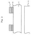
- Figures 1 and 2 show the sectional configurations of the shield materials.
- the shield material of Figure 1 is composed of a black metallic oxide layer 2 and a metallic layer 3 successively formed in identical laminated mesh-like configuration on a transparent base plate 1 by ion plating.
- the shield material of Figure 2 is composed of a metallic layer 3 and a black metallic oxide layer 2 also successively formed in identical laminated mesh-like configuration by ion plating.
- the metallic layer 3 of the two layers is located on the side of a display 4.
- IP ion-plated
- IP copper layer metallic layer: 1.5 ⁇ m
- Etching resist was then formed on the metallic layer in a grid-like pattern (line width: 20 ⁇ m, line interval: 180 ⁇ m, thickness: 5 ⁇ m).
- etching solution aqueous solution of 20 % ferric chloride and 1.75 % hydrochloric acid
- etching solution aqueous solution of 20 % ferric chloride and 1.75 % hydrochloric acid
- the electromagnetic radiation shield material exhibited high shielding performance of 60 dB (500 MHz) and transparency (optical transmittance) of 75 %. It was also excellent in clarity (the black layer was high in degree of blackness and free of unevenness) and had a broad viewing angle.
- a transparent electromagnetic radiation shield material was fabricated in the same manner as in Example 1, except that the order of the IP treatment was reversed (i.e., the IP copper was formed on the glass plate first and the IP tin oxide was then formed on the IP copper).
- the transparent electromagnetic radiation shield material exhibited good performance like that of Example 1.
- Transparent electromagnetic radiation shield materials were fabricated in the manner of Example 1 without changing the aperture ratio of the grid-like pattern from that in Example 1 (line width: 20 ⁇ m, line interval: 180 ⁇ m, aperture ratio: 81 %) but with the line width and line interval narrowed to 1/2 (Example 3) and 1/4 (Example 4).
- a transparent electromagnetic radiation shield material was fabricated in the manner of Example 1, except that the aperture ratio of the grid-like pattern was increased to obtain an electromagnetic radiation shield material with narrower line interval and width (line width: 3 ⁇ m, line interval: 45 ⁇ m, aperture ratio: 87 %).
- This electromagnetic radiation shield material was superior to that of Example 1 in transparency (optical transmittance) and shielding performance.
- resist was formed on the glass plate in a reverse-grid-like pattern, the two layers were laminated in the manner of Example 1, the result was immersed in a defoliating solution, and the resist (with the two layers thereon) was removed by peeling.
- This electromagnetic radiation shield material was superior to that of Example 1 in degree of finish (processing precision). Its other performances were the same as that of Example 1. As the method of this example involves many fewer processing steps and achieves higher yield that of Example 1, it can provide a low-cost product.
- a transparent electromagnetic radiation shield material was fabricated in the manner of Example 1, except that a polyethylene terephthalate (PET) film was used in place of the glass plate.
- PET polyethylene terephthalate
- the transparent electromagnetic radiation shield material exhibited good performance like that of Example 1. Clarity was particularly good when the electromagnetic radiation shield material was laminated directly on the display panel. (A shield material having a mesh-like pattern can be spaced from the display panel up to a distance than does not cause blurring to an annoying degree, but since blurring increases with increasing distance, the clarity is inferior to that in the case of direct lamination.)
- a transparent electromagnetic radiation shield material was fabricated in the manner of Example 1, except that a PET film was used in place of the glass plate and the metallic layer was not formed of a single IP copper layer (1.5 ⁇ m) but of three layers: an IP chromium layer (0.1 ⁇ m), an IP copper layer (1.5 ⁇ m) and an IP chromium layer (0.1 ⁇ m).
- the transparent electromagnetic radiation shield material exhibited good performance like that of Example 1.
- a panel obtained by laminating the electromagnetic radiation shield material onto a transparent plate was tested, it was found to exhibit chromium luster and excellent clarity even when spaced apart from the display panel as in the case of Example 1. (Copper luster tends to degrade image quality.)
- the sandwiching of the copper layer between the chromium layers not only provided the early enhancement in shielding performance but by imparting corrosion resistance also improved the long-term stability of the shielding performance.
- a transparent electromagnetic radiation shield material was fabricated in the manner of Example 8, except that the black metallic oxide layer and the metallic layer were formed by sputtering (SP) rather than ion plating (IP).
- SP sputtering
- IP ion plating
- a copper foil (9 ⁇ m) was laminated on a PET film via a transparent acrylic resin adhesive and was then etched into a grid-like pattern by the method of Example 2. Electroplating with blackish nickel (1-1.5 ⁇ m) was then conducted to obtain a transparent electromagnetic radiation shield material with a gray-to-black copper foil pattern surface.
- This electromagnetic radiation shield material was excellent ⁇ as good as or better than that in Example 2 ⁇ but its clarity was markedly poorer than that in Example 2 owing to the insufficient and uneven degree of blackness of the copper foil pattern surface. Its transparency (optical transmittance) was also lower than that in Example 2 (even when a transparent resin coating was formed after etching and electroplating) because the black electrodeposited layer was also deposited on the side surface of the copper foil pattern (thereby reducing the aperture ratio).
- the optical transmittance was extremely low because transparency was degraded by back-transfer of the copper foil roughness to the adhesive surface region after etching and electroplating.
- the black electrodeposited material was from place to place deposited over the entire aperture portion (clogging occurred), making the appearance unacceptable (black spot defects).
- a transparent electromagnetic radiation shield material was fabricated in the manner of Comparative Example 1, except that instead of laminating the copper foil on the PET film, an IP copper layer (1.5 ⁇ m) was formed directly on the PET film.
- the shielding performance of this electromagnetic radiation shield material was excellent ⁇ on a par with that in Example 2 ⁇ but its clarity was about the same as that in Comparative Example 1, i.e., markedly poorer than that in Example 2.
- Its transparency (optical transmittance) was higher than that in Comparative Example 1 by an amount attributable to the absence of the adhesive layer and the transparent resin coating but lower than that in Example 2 because, like in Comparative Example 1, the black electrodeposited layer was also deposited on the side surface of the IP copper pattern.
- many defects in appearance were observed after formation of the black electrodeposited layer.
- a copper foil (9 ⁇ m) was laminated on a PET film via a transparent acrylic adhesive, the surface of the copper foil was made brown-black by chemical treatment (a copper oxide layer was formed to a depth of 2-3 ⁇ m from the copper foil surface), and the copper foil was formed into a grid-like pattern by the method of Example 2 to afford a transparent electromagnetic radiation shield material.
- This electromagnetic radiation shield material was excellent ⁇ as good as or better than that in Example 2 ⁇ but its clarity was markedly inferior to that of Example 2 owing to the insufficient and uneven degree of blackness of the copper foil surface.
- its transparency optical transmittance
- a transparent electromagnetic radiation shield material was fabricated in the manner of Comparative Example 3, except that instead of laminating a copper foil on a PET film, an IP copper layer (1.5 ⁇ m) was formed directly on the PET film. The copper oxide layer was formed to a depth of 0.5-1 ⁇ m from the IP copper layer surface.
- a copper foil (9 ⁇ m) chemically treated to form a copper oxide layer (brown-black) to a depth of 2-3 ⁇ m from the surface was laminated on a PET film via a transparent acrylic resin adhesive.
- the copper foil of the laminated article was etched into a grid-like pattern (line width: 40 ⁇ m, line interval: 360 ⁇ m, aperture ratio 81 %) in the manner of Example 1 and then formed with a transparent resin coating to afford a transparent electromagnetic radiation shield material.
- a transparent electromagnetic radiation shield material was fabricated in the manner of Comparative Example 5, except that copper foil had a thickness of 35 ⁇ m instead of 9 ⁇ m.
- the electromagnetic radiation shield material Owing to considerable thickness of the copper foil, the electromagnetic radiation shield material exhibited excellent shielding performance on a par with that in Example 1 despite the broad line interval of 360 ⁇ m, but its clarity and transparency (optical transmittance) were the same as those in Comparative Example 3 and poorer than those in Example 1.
Landscapes
- Engineering & Computer Science (AREA)
- Manufacturing & Machinery (AREA)
- Physics & Mathematics (AREA)
- Plasma & Fusion (AREA)
- Microelectronics & Electronic Packaging (AREA)
- Shielding Devices Or Components To Electric Or Magnetic Fields (AREA)
- Laminated Bodies (AREA)
Applications Claiming Priority (2)
| Application Number | Priority Date | Filing Date | Title |
|---|---|---|---|
| JP33833099 | 1999-10-25 | ||
| JP33833099A JP2001127485A (ja) | 1999-10-25 | 1999-10-25 | 透視性電磁波シールド材及びその製造方法 |
Publications (1)
| Publication Number | Publication Date |
|---|---|
| EP1096845A1 true EP1096845A1 (de) | 2001-05-02 |
Family
ID=18317143
Family Applications (1)
| Application Number | Title | Priority Date | Filing Date |
|---|---|---|---|
| EP00308811A Withdrawn EP1096845A1 (de) | 1999-10-25 | 2000-10-06 | Transparentes Material zur Abschirmung gegen elektromagnetische Strahlung und dessen Herstellungsverfahren |
Country Status (3)
| Country | Link |
|---|---|
| EP (1) | EP1096845A1 (de) |
| JP (1) | JP2001127485A (de) |
| CA (1) | CA2324169A1 (de) |
Cited By (4)
| Publication number | Priority date | Publication date | Assignee | Title |
|---|---|---|---|---|
| EP1215705A3 (de) * | 2000-12-12 | 2003-05-21 | Nisshinbo Industries, Inc. | Durchsichtiges Abschirmmaterial gegen elektromagnetische Strahlung |
| WO2004039137A1 (ja) * | 2002-10-25 | 2004-05-06 | Nikko Materials Co., Ltd. | プラズマディスプレーパネル用銅箔及びその製造方法 |
| US10649592B2 (en) | 2015-06-26 | 2020-05-12 | Sumitomo Metal Mining Co., Ltd. | Conductive substrate and method for fabricating conductive substrate |
| US10655209B2 (en) | 2013-03-21 | 2020-05-19 | Noritake Co., Limited | Electromagnetic shield |
Families Citing this family (12)
| Publication number | Priority date | Publication date | Assignee | Title |
|---|---|---|---|---|
| JP2002341780A (ja) * | 2001-05-16 | 2002-11-29 | Bridgestone Corp | 電磁波シールド性光透過窓材 |
| JP2006140205A (ja) * | 2004-11-10 | 2006-06-01 | Toppan Printing Co Ltd | 電磁波遮蔽材およびその製造方法、ならびにディスプレイ用フィルム |
| KR100710540B1 (ko) * | 2005-04-01 | 2007-04-24 | 엘에스전선 주식회사 | 고분자 필름 상에 흑색 전기도금층 패턴이 형성된 전자파차폐재 |
| KR100710541B1 (ko) * | 2005-04-01 | 2007-04-25 | 엘에스전선 주식회사 | 고분자 필름 상에 흑색 전기도금층 패턴이 형성된 전자파차폐재의 제조방법 |
| JP2007030394A (ja) * | 2005-07-28 | 2007-02-08 | Sumitomo Osaka Cement Co Ltd | 光学構造体及びその製造方法並びにそれを備えた表示装置 |
| JP2008012916A (ja) * | 2006-06-08 | 2008-01-24 | Hitachi Via Mechanics Ltd | 複合シート、複合シートの加工方法、及びレーザ加工装置 |
| US20100206628A1 (en) * | 2006-09-04 | 2010-08-19 | Toray Industries, Inc. | Transparent electromagnetic wave shield member and method for manufacturing the same |
| JP5151425B2 (ja) * | 2007-12-03 | 2013-02-27 | 東レ株式会社 | ディスプレイ用フィルター及びその製造方法 |
| CN102303429B (zh) * | 2011-06-21 | 2014-04-09 | 电子科技大学 | 一种可调谐的平板电磁波吸收材料 |
| CN103669780B (zh) * | 2013-12-06 | 2015-12-02 | 江苏高博智融科技有限公司 | 一种具有屏蔽电磁波功能的墙纸 |
| JP6601137B2 (ja) * | 2015-10-16 | 2019-11-06 | 住友金属鉱山株式会社 | 積層体基板、積層体基板の製造方法、導電性基板、及び導電性基板の製造方法 |
| JP2019016782A (ja) * | 2017-07-03 | 2019-01-31 | 信越ポリマー株式会社 | 電磁波シールドフィルム及びその製造方法、並びに電磁波シールドフィルム付きプリント配線板及びその製造方法 |
Citations (3)
| Publication number | Priority date | Publication date | Assignee | Title |
|---|---|---|---|---|
| JPH10335883A (ja) * | 1997-05-27 | 1998-12-18 | Gunze Ltd | 電磁波シールド用透明部材 |
| EP0914033A2 (de) * | 1997-09-29 | 1999-05-06 | Nisshinbo Industries Inc. | Elektromagnetische Strahlung abschirmende Material und Platte, sowie deren Herstellungsverfahren |
| EP1024683A2 (de) * | 1999-01-28 | 2000-08-02 | Nisshinbo Industries, Inc. | Transparantes Material zur Abschirmung gegen elektromagnetische Strahlung und dessen Herstellungsverfahren |
-
1999
- 1999-10-25 JP JP33833099A patent/JP2001127485A/ja active Pending
-
2000
- 2000-10-06 EP EP00308811A patent/EP1096845A1/de not_active Withdrawn
- 2000-10-24 CA CA002324169A patent/CA2324169A1/en not_active Abandoned
Patent Citations (3)
| Publication number | Priority date | Publication date | Assignee | Title |
|---|---|---|---|---|
| JPH10335883A (ja) * | 1997-05-27 | 1998-12-18 | Gunze Ltd | 電磁波シールド用透明部材 |
| EP0914033A2 (de) * | 1997-09-29 | 1999-05-06 | Nisshinbo Industries Inc. | Elektromagnetische Strahlung abschirmende Material und Platte, sowie deren Herstellungsverfahren |
| EP1024683A2 (de) * | 1999-01-28 | 2000-08-02 | Nisshinbo Industries, Inc. | Transparantes Material zur Abschirmung gegen elektromagnetische Strahlung und dessen Herstellungsverfahren |
Non-Patent Citations (1)
| Title |
|---|
| PATENT ABSTRACTS OF JAPAN vol. 1999, no. 03 31 March 1999 (1999-03-31) * |
Cited By (4)
| Publication number | Priority date | Publication date | Assignee | Title |
|---|---|---|---|---|
| EP1215705A3 (de) * | 2000-12-12 | 2003-05-21 | Nisshinbo Industries, Inc. | Durchsichtiges Abschirmmaterial gegen elektromagnetische Strahlung |
| WO2004039137A1 (ja) * | 2002-10-25 | 2004-05-06 | Nikko Materials Co., Ltd. | プラズマディスプレーパネル用銅箔及びその製造方法 |
| US10655209B2 (en) | 2013-03-21 | 2020-05-19 | Noritake Co., Limited | Electromagnetic shield |
| US10649592B2 (en) | 2015-06-26 | 2020-05-12 | Sumitomo Metal Mining Co., Ltd. | Conductive substrate and method for fabricating conductive substrate |
Also Published As
| Publication number | Publication date |
|---|---|
| JP2001127485A (ja) | 2001-05-11 |
| CA2324169A1 (en) | 2001-04-25 |
Similar Documents
| Publication | Publication Date | Title |
|---|---|---|
| US6433481B1 (en) | Transparent electromagnetic radiation shield material | |
| EP1096845A1 (de) | Transparentes Material zur Abschirmung gegen elektromagnetische Strahlung und dessen Herstellungsverfahren | |
| JP5667938B2 (ja) | 静電容量方式タッチパネル | |
| JP6698064B2 (ja) | 導電層付き基板、タッチパネル用透明電極付き基板及びそれらの製造方法 | |
| JPWO2008029776A1 (ja) | 光透過性電磁波シールド部材およびその製造方法 | |
| KR20000016876A (ko) | 전자파차폐투명체 | |
| EP1215705A2 (de) | Durchsichtiges Abschirmmaterial gegen elektromagnetische Strahlung | |
| US6188174B1 (en) | Electromagnetic radiation shield panel and method of producing the same | |
| US6713161B1 (en) | Light-transmitting electromagnetic shielding material and method for manufacturing the same | |
| CA2359312A1 (en) | Transparent electromagnetic radiation shield/near infrared ray cut material and methods of producing the same | |
| JP6445365B2 (ja) | 透視性電極、該透視性電極を用いてなるタッチパネル用位置検知電極、タッチパネル、及び画像表示装置 | |
| WO2018047493A1 (ja) | 導電性フィルム、タッチパネルセンサー、および、タッチパネル | |
| TW201901701A (zh) | 透明導電性基板之製造方法、透明導電性基板 | |
| JPWO2003045125A1 (ja) | 電磁波シールド性光透過窓材及びその製造方法 | |
| US6143674A (en) | Electromagnetic radiation shield material and panel and methods of producing the same | |
| JP2002246788A (ja) | 透視性電磁波シールド材 | |
| JP2979021B2 (ja) | 透視性電磁波シールド材料とその製造方法 | |
| JP2004241761A (ja) | 電磁波遮蔽用シート、及びその製造方法 | |
| JPWO2003045127A1 (ja) | 電磁波シールド性光透過窓材及びその製造方法 | |
| JP2000040896A (ja) | 電磁波遮蔽材、その製造方法および電磁波シールド対策製品 | |
| JPH10335883A (ja) | 電磁波シールド用透明部材 | |
| JP4629969B2 (ja) | 電磁波シールド用銅箔、その製造方法、および該銅箔で作成した電磁波シールド体 | |
| JPH11163587A (ja) | 電磁波シールド材、パネル及び製造方法 | |
| JP2006210763A (ja) | ディスプレイ用電磁波シールドフィルタ | |
| KR20070113161A (ko) | 도금형 광학 필터 및 이의 제조 방법 |
Legal Events
| Date | Code | Title | Description |
|---|---|---|---|
| PUAI | Public reference made under article 153(3) epc to a published international application that has entered the european phase |
Free format text: ORIGINAL CODE: 0009012 |
|
| AK | Designated contracting states |
Kind code of ref document: A1 Designated state(s): DE FR GB |
|
| AX | Request for extension of the european patent |
Free format text: AL;LT;LV;MK;RO;SI |
|
| 17P | Request for examination filed |
Effective date: 20010621 |
|
| AKX | Designation fees paid |
Free format text: DE FR GB |
|
| STAA | Information on the status of an ep patent application or granted ep patent |
Free format text: STATUS: THE APPLICATION HAS BEEN WITHDRAWN |
|
| 18W | Application withdrawn |
Withdrawal date: 20020909 |