EP1098213A1 - Verfahren zur Herstellung von Faserschwanz-arrays - Google Patents
Verfahren zur Herstellung von Faserschwanz-arrays Download PDFInfo
- Publication number
- EP1098213A1 EP1098213A1 EP99402722A EP99402722A EP1098213A1 EP 1098213 A1 EP1098213 A1 EP 1098213A1 EP 99402722 A EP99402722 A EP 99402722A EP 99402722 A EP99402722 A EP 99402722A EP 1098213 A1 EP1098213 A1 EP 1098213A1
- Authority
- EP
- European Patent Office
- Prior art keywords
- optical waveguide
- optical
- alignment
- fibers
- grooves
- Prior art date
- Legal status (The legal status is an assumption and is not a legal conclusion. Google has not performed a legal analysis and makes no representation as to the accuracy of the status listed.)
- Withdrawn
Links
- 238000003491 array Methods 0.000 title claims description 10
- 238000004519 manufacturing process Methods 0.000 title claims description 10
- 230000003287 optical effect Effects 0.000 claims abstract description 140
- 230000008054 signal transmission Effects 0.000 claims abstract description 8
- 239000000835 fiber Substances 0.000 claims description 73
- VYPSYNLAJGMNEJ-UHFFFAOYSA-N Silicium dioxide Chemical compound O=[Si]=O VYPSYNLAJGMNEJ-UHFFFAOYSA-N 0.000 claims description 64
- 239000013307 optical fiber Substances 0.000 claims description 56
- 239000000758 substrate Substances 0.000 claims description 47
- 239000000853 adhesive Substances 0.000 claims description 38
- 230000001070 adhesive effect Effects 0.000 claims description 38
- XUIMIQQOPSSXEZ-UHFFFAOYSA-N Silicon Chemical compound [Si] XUIMIQQOPSSXEZ-UHFFFAOYSA-N 0.000 claims description 34
- 229910052710 silicon Inorganic materials 0.000 claims description 34
- 239000010703 silicon Substances 0.000 claims description 34
- 239000000377 silicon dioxide Substances 0.000 claims description 32
- 238000000034 method Methods 0.000 claims description 30
- 239000011347 resin Substances 0.000 claims description 15
- 229920005989 resin Polymers 0.000 claims description 15
- 238000005530 etching Methods 0.000 claims description 14
- 238000000206 photolithography Methods 0.000 claims description 9
- 238000000151 deposition Methods 0.000 claims description 8
- 238000001020 plasma etching Methods 0.000 claims description 8
- 238000000576 coating method Methods 0.000 claims description 6
- 239000011248 coating agent Substances 0.000 claims description 5
- 238000004140 cleaning Methods 0.000 claims 1
- 230000000873 masking effect Effects 0.000 description 23
- 239000010410 layer Substances 0.000 description 17
- 239000000463 material Substances 0.000 description 17
- 230000008569 process Effects 0.000 description 12
- 238000013459 approach Methods 0.000 description 11
- 235000012431 wafers Nutrition 0.000 description 11
- 238000003754 machining Methods 0.000 description 9
- 230000008901 benefit Effects 0.000 description 8
- 230000009471 action Effects 0.000 description 7
- 238000005520 cutting process Methods 0.000 description 7
- 238000001723 curing Methods 0.000 description 5
- 238000012986 modification Methods 0.000 description 5
- 230000004048 modification Effects 0.000 description 5
- 238000005498 polishing Methods 0.000 description 4
- 239000011253 protective coating Substances 0.000 description 4
- 238000003486 chemical etching Methods 0.000 description 3
- 230000007423 decrease Effects 0.000 description 3
- 238000013461 design Methods 0.000 description 3
- 230000008878 coupling Effects 0.000 description 2
- 238000010168 coupling process Methods 0.000 description 2
- 238000005859 coupling reaction Methods 0.000 description 2
- 238000007872 degassing Methods 0.000 description 2
- 230000001419 dependent effect Effects 0.000 description 2
- 230000007246 mechanism Effects 0.000 description 2
- 230000015572 biosynthetic process Effects 0.000 description 1
- 239000007795 chemical reaction product Substances 0.000 description 1
- 238000004891 communication Methods 0.000 description 1
- 230000001186 cumulative effect Effects 0.000 description 1
- 230000007547 defect Effects 0.000 description 1
- 230000008021 deposition Effects 0.000 description 1
- 238000010586 diagram Methods 0.000 description 1
- 230000000694 effects Effects 0.000 description 1
- 238000004049 embossing Methods 0.000 description 1
- 230000003628 erosive effect Effects 0.000 description 1
- 239000011521 glass Substances 0.000 description 1
- 238000005259 measurement Methods 0.000 description 1
- 238000000465 moulding Methods 0.000 description 1
- 238000004806 packaging method and process Methods 0.000 description 1
- 229920001296 polysiloxane Polymers 0.000 description 1
- 239000011241 protective layer Substances 0.000 description 1
- 230000005855 radiation Effects 0.000 description 1
- 238000004513 sizing Methods 0.000 description 1
- 239000000126 substance Substances 0.000 description 1
- 238000001029 thermal curing Methods 0.000 description 1
- 238000001039 wet etching Methods 0.000 description 1
Images


Classifications
-
- G—PHYSICS
- G02—OPTICS
- G02B—OPTICAL ELEMENTS, SYSTEMS OR APPARATUS
- G02B6/00—Light guides; Structural details of arrangements comprising light guides and other optical elements, e.g. couplings
- G02B6/24—Coupling light guides
- G02B6/36—Mechanical coupling means
- G02B6/3628—Mechanical coupling means for mounting fibres to supporting carriers
- G02B6/3632—Mechanical coupling means for mounting fibres to supporting carriers characterised by the cross-sectional shape of the mechanical coupling means
- G02B6/3636—Mechanical coupling means for mounting fibres to supporting carriers characterised by the cross-sectional shape of the mechanical coupling means the mechanical coupling means being grooves
-
- G—PHYSICS
- G02—OPTICS
- G02B—OPTICAL ELEMENTS, SYSTEMS OR APPARATUS
- G02B6/00—Light guides; Structural details of arrangements comprising light guides and other optical elements, e.g. couplings
- G02B6/24—Coupling light guides
- G02B6/36—Mechanical coupling means
- G02B6/3628—Mechanical coupling means for mounting fibres to supporting carriers
- G02B6/3648—Supporting carriers of a microbench type, i.e. with micromachined additional mechanical structures
- G02B6/3652—Supporting carriers of a microbench type, i.e. with micromachined additional mechanical structures the additional structures being prepositioning mounting areas, allowing only movement in one dimension, e.g. grooves, trenches or vias in the microbench surface, i.e. self aligning supporting carriers
-
- G—PHYSICS
- G02—OPTICS
- G02B—OPTICAL ELEMENTS, SYSTEMS OR APPARATUS
- G02B6/00—Light guides; Structural details of arrangements comprising light guides and other optical elements, e.g. couplings
- G02B6/24—Coupling light guides
- G02B6/36—Mechanical coupling means
- G02B6/3628—Mechanical coupling means for mounting fibres to supporting carriers
- G02B6/3684—Mechanical coupling means for mounting fibres to supporting carriers characterised by the manufacturing process of surface profiling of the supporting carrier
- G02B6/3692—Mechanical coupling means for mounting fibres to supporting carriers characterised by the manufacturing process of surface profiling of the supporting carrier with surface micromachining involving etching, e.g. wet or dry etching steps
-
- G—PHYSICS
- G02—OPTICS
- G02B—OPTICAL ELEMENTS, SYSTEMS OR APPARATUS
- G02B6/00—Light guides; Structural details of arrangements comprising light guides and other optical elements, e.g. couplings
- G02B6/24—Coupling light guides
- G02B6/26—Optical coupling means
- G02B6/30—Optical coupling means for use between fibre and thin-film device
-
- G—PHYSICS
- G02—OPTICS
- G02B—OPTICAL ELEMENTS, SYSTEMS OR APPARATUS
- G02B6/00—Light guides; Structural details of arrangements comprising light guides and other optical elements, e.g. couplings
- G02B6/24—Coupling light guides
- G02B6/36—Mechanical coupling means
- G02B6/38—Mechanical coupling means having fibre to fibre mating means
- G02B6/3807—Dismountable connectors, i.e. comprising plugs
- G02B6/3873—Connectors using guide surfaces for aligning ferrule ends, e.g. tubes, sleeves, V-grooves, rods, pins, balls
- G02B6/3885—Multicore or multichannel optical connectors, i.e. one single ferrule containing more than one fibre, e.g. ribbon type
Definitions
- the present invention relates generally to optical waveguide connectors, and more particularly to a connector of an array of optical waveguides.
- Optical waveguide arrays may generally be described as the gathering and positioning of the ends of multiple optical fibers into a specific pattern.
- Optical waveguide arrays may serve as input terminals, output terminals and interstage couplers for optical communication systems.
- Precision fiber optic arrays are important components of such systems.
- the alignment of arrays of optical waveguides to one another is a challenging endeavor that has engendered many diverse approaches.
- Of particular interest in is the combining multiple optical waveguides in the form of optical fibers into arrays in order to reduce the number of separate connectors required and to simplify the connection process.
- Most current approaches to the design of optical waveguide arrays focus on the use of V-grooves for aligning the optical fibers. In particular these approaches use the sides of the V-grooves as the primary vehicle for the horizontal and vertical positioning of the optical fibers.
- One proposed approach involves the machining of grooves into a substrate block, and then cutting the substrate block into a number of smaller grooved blocks. Typically this process is used to machine V-grooves into the substrate blocks.
- the standard pitch for grooves obtained by machining is 250 ⁇ m.
- Standard optical fibers presently in use are on the order of 125 ⁇ m in diameter, therefore, machined grooves do not allow for the smallest packaging possible.
- a number of obstacles to obtaining the precision required in optical connections are inherent in this machining process. The machining of the grooves and the subsequent cutting of the substrate into smaller units may lead to warpage of the substrate block.
- any machining process involves the removal of material not only from the object being machined, but also from the cutters removing the material.
- This erosion of the cutting tools results in a loss of precision in both the width and depth of the machined grooves.
- the accuracy obtainable using this machining approach is highly dependent upon the depth and pitch control of the cutting machine, as well as the wear characteristics of the cutters used.
- the precision with which each groove may be located decreases. This decrease in groove location accuracy is due to the fact that each groove is typically cut individually. Therefore, the positioning tolerances and resolution of the cutting machine come into play.
- the effect of positioning tolerance and measurement resolution is cumulative, increasing in direct proportion to the number of separate positions the cutting machine must be set up in.
- Chemical etching of silicon is another proposed approach. Chemical etching, also referred to as wet etching, is typically done using silicon wafers in clean rooms. This process involves partially masking a silicon wafer with a desired pattern and then exposing the masked silicon wafer to a reactive chemical that removes material from the wafer in areas not protected by the mask. The chemical etching of silicone wafers results in V-grooves due to the crystalline structure of the silicon. Photolithography is typically used to lay out the mask pattern and is capable of producing patterns with very high V-groove densities.
- the precision of the location if the V-grooves does not depend on the number of V-grooves being etched, but rather on the precision of the masking.
- the wafer is sectioned into blocks for use in making optical fiber arrays. Sectioning of the wafers into blocks requires the use of precision machine tools, and close tolerance cutters.
- the operational steps of the etching, sectioning and assembly require the design of specialized assembly equipment. In order to be cost effective, the high cost associated with specialized machinery necessitates this approach can only be used for high volume production.
- Another proposed approach involves the embossing of grooves in a glass material.
- One aspect of the present invention relates to an optical waveguide alignment device for use with a plurality of optical waveguide fibers.
- Each fiber has a bare portion and a covered portion.
- the fibers are configured to transmit an optical signal.
- the optical waveguide alignment device includes a substrate having a substantially planar surface.
- the substantially planar surface is a grooved surface having a plurality of grooves.
- Each groove has a substantially rectangular shape and a portion of lesser dimension than the diameter of the bared portion of one of the optical waveguide fibers.
- Each of these portions is configured to support one of the optical waveguide fibers in a predetermined position.
- the invention in another aspect, includes an optical waveguide alignment device for use with a plurality of optical waveguide fibers, each fiber having a bare portion and a covered portion.
- the fibers are configured to transmit an optical signal.
- the optical waveguide alignment device includes a substrate having a substantially planar surface where the planar surface has a number of grooves. These grooves vary in width. Each groove has a substantially rectangular shape. These grooves have a first narrow portion and a second narrow portion with an intermediate portion disposed therebetween. The first and the second narrow portion are lesser in width than the diameter of the bared portions of one of the optical waveguide fibers that is to be positioned.
- the invention in another aspect, includes a connector for optical signal transmission systems for use with a plurality of optical waveguide fibers.
- Each fiber includes a bare portion and a covered portion, and is configured to transmit an optical signal therethrough.
- the bare portion has a terminal end configured for emitting or receiving light.
- the connector for optical signal transmission systems includes an alignment base plate having a connection face, and a grooved surface adjacent to the connection face and forming an angle with the connection face.
- the grooved surface includes a plurality of coplanar grooves.
- Each groove including a proximate portion adjacent to the connecting face having a substantially rectangular cross section lesser in width than the diameter of the bare portion of the optical fiber, a distal portion having a substantially rectangular cross section lesser in width than the diameter of the bare portion of the optical fiber, and an intermediate portion having a substantially rectangular cross section therebetween.
- the intermediate portion havs a width greater than the widths of the proximate and distal portions.
- An alignment top plate is attached to the alignment base plate , the alignment top plate has a connection face and a grooved surface adjacent to the connection face which forms an angle with the connection face.
- the grooved surface including a plurality of coplanar grooves.
- Each groove including a proximate portion adjacent to the connecting face having a substantially rectangular cross section lesser in width than the diameter of the bare portion of the optical fiber, a distal portion having a substantially rectangular cross section lesser in width than the diameter of the bare portion of the optical fiber, and an intermediate portion having a substantially rectangular cross section therebetween.
- the intermediate portion has a width greater than the widths of the proximate and the distal portions.
- the alignment base plate and the alignment top plate support and restrain each of the plurality of optical waveguide fibers in a predetermined position, and the connection face of the alignment base plate and the connection face of the alignment top plate are positioned to form a substantially planar surface.
- the substantially planar surface is configured to facilitate use of the optical fibers as providers of input signals to or receivers of output signals from an optical device.
- the invention includes a method for manufacturing optical waveguide alignment devices.
- This method includes the steps of: forming a body having a planar surface, forming a number of grooves in the planar surface, severing the body to form at least two grooved supports, inserting a number of optical waveguides into the waveguide fibers into the grooves of the first groove support, and placing the second grooved support on the first grooved support, thereby aligning the optical waveguides with the grooves in the first and second supports.
- the first grooved support is attached to the second grooved support and the optical waveguides to form an optical waveguide block.
- a portion is removed from the optical waveguide block, where the removal takes place along a plane transverse to the plurality of optical waveguides and produces at least one surface.
- the ends of the optical waveguide fibers terminate and are coplanar with this surface and this surface is suitable for use as an optical connection surface.
- the invention in another aspect, relates to a method for manufacturing optical waveguide alignment devices for an optical signal transmission system, including the steps of: forming a silica substrate block depositing a silicon masking layer on the substrate block, depositing a resin masking layer, curing the resin masking layer, etching the masking layer, etching the substrate block, removing the silicon mask, placing a protective coating on the etched silica substrate block, severing the etched silica substrate block into a number of fiber guide blocks, removing the coating, selecting two complimentary fiber guide blocks, sandwiching a plurality of optical fibers between the selected guide blocks, inserting an adhesive to attach the guide blocks to each other and the optical waveguide fibers, and polishing a face of the guide block to serve as an optical interface.
- the invention includes a method for manufacturing optical waveguide alignment devices.
- This method includes the steps of: forming a body having a planar surface, forming a number of grooves in the planar surface, and severing the body to form at least two grooved supports.
- a number of optical waveguide are then inserted into the grooves of the first grooved support.
- the second grooved support is placed on the first grooved support, aligning the optical waveguides with the grooves of the first and second supports.
- the first grooved support is attached to the second grooved support and the optical waveguides to form an optical waveguide block.
- a portion is removed from the optical waveguide block, where the removal takes place along a plane transverse to the plurality of optical waveguides and produces at least one surface.
- the ends of the optical waveguide fibers terminate and are coplanar with this surface and this surface is suitable for use as an optical connection surface.
- the invention in another aspect, relates to a method for manufacturing optical waveguide alignment devices for an optical signal transmission system, including the steps of: forming a silica substrate block, depositing a silicon masking layer on the substrate block, depositing a resin masking layer, curing the resin masking layer, etching the masking layer, etching the substrate block, removing the silicon mask, placing a protective coating on the etched silica substrate block, severing the etched silica substrate block into a number of fiber guide blocks, removing the coating, selecting two complimentary fiber guide blocks, sandwiching a plurality of optical fibers between selective guide blocks, inserting an adhesive to attach the guide blocks to each other and the fibers, and polishing a base of the guide block to serve as an optical interface.
- the optical alignment device of the present invention results in a number of advantages over the prior art.
- the use of photolithography allows the precise layout of the grooves.
- the precision layout increases the number of waveguides that may be positioned by a single optical alignment device. This increase in the number of waveguides is due to the dramatic decrease in positioning error when compared to other proposed methods of manufacture.
- the advantages conferred by the present invention over the prior art is the use of rectangular shaped grooves for the containment and alignment of the optical fibers in a predetermined pattern.
- the use of rectangular shaped grooves allows for increased precision in the positioning of the optical fibers. This is accomplished by utilizing the edges of the grooves as contact points rather than the flats of the sides or bottom of the grooves as done in other proposed methods.
- Still another advantage of an embodiment of the present invention over the prior art is that only one alignment plate is necessary when configured with the rectangular shaped grooves. This is because the rectangular shaped grooves allow the precise alignment in a vertical dimension from a planar surface of the optical fiber ends sought to be coupled to an optical device. This advantage is further illustrated in that no cover plate is required, thereby removing an assembly step and an extra part from the assembly.
- Another example of an advantage of an embodiment of the present invention is the contact points for the bare portion of fiber are line contacts along the edges of the "U" shaped grooves, rather than the flats of the "V" grooves used in the prior art. The lines of contact minimizes the contact area of the bare portion of the optical fiber with the grooves, while providing for the precise alignment and positioning of the fibers.
- Another advantage of an embodiment of the present invention over the prior art is the use of grooves of varying width.
- the variation in the width of the grooves allow both the alignment of the bare portion of the fiber from which signals will be transmitted and received and of the covered portion of the fiber.
- the support of the cover portion of the fiber allows a more robust design of the optical alignment device when it is used in an optical connection capacity.
- Yet another advantage of an embodiment of the present invention over the prior art is the use of reactive ion etching, which allows the substrate material of the optical alignment device component blocks to be manufactured from either silica or silicon.
- silica is a media that is transparent to ultra-violet radiation. Therefore, an ultra-violet curable adhesive may be used. The use of the ultra-violet adhesive does away with the necessity of the thermally curing the adhesive.
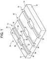
- Figure 1 is a perspective view of the optical fiber alignment device in which the present invention is embodied.
- Figure 2 is a front plan view of the optical fiber alignment device shown in Fig. 1.
- Figure 3 is an enlarged fragmentary detail view of the portion of the optical fiber alignment device within the cited circle "AA" of Fig. 2.
- Figure 4 is a perspective view of an alternative embodiment of the optical fiber alignment device in which the present invention is embodied.
- Figure 5 is a side elevation view of the optical fiber alignment device as shown in fig. 4.
- Figure 6 is a flow chart showing the fabrication process steps of the present invention in block diagram form.
- FIG. 1 An exemplary body of the optical fiber alignment block of the present invention is shown in Fig. 1 and is designated generally throughout by reference numeral 10.
- the present invention for an optical waveguide alignment device 10 includes a substrate 12.
- the substrate 12 should have similar mechanical and thermal properties to the material to which the optical alignment device 10 will be connected.
- Exemplary of such items that the optical alignment device 10 may be connected to are optical cross connect switches, optical pigtails, lightwave optical circuits, planar devices, other optical alignment devices, and any other device that it is desired to make a connection of a plurality of optical fibers held in precise positions to.
- Exemplary of the materials from which the substrate 12 may be made are silica and silicon.
- the substrate 12 includes a grooved surface 14 that contains a plurality of grooves 16.
- the grooves 16 are formed in the substrate 12 by the use of photolithography and an etching process. Exemplary of this is the use of a reactive ion etching process with a silica or silicon substrate.
- Each of the grooves 16 has a first end portion 30 and a second end portion 32 separated by an intermediate portion 28.
- the grooves 16 are to and position the bare portion 42 of optical fibers 40.
- the bare portion 42 of the optical fiber 40 is contacted along its circumference by the edges 62 of the first end portion 30 and the edges 64 of the second end portion 32 of the groove 16.
- the edges 66 of the intermediate portion 28 of the groove 16 do not contact the bare portion 42 of the fiber 40.
- Each of the grooves 16 has a depth 26 which is determined by the amount of time in which the reactive ion etching process is used.
- the depth 26 of the groove 16 is dependent upon the lesser of the width 34 of the first end portion 30 and the width 36 of the second end portion 32 of the groove 16.
- the depth 26 of the groove 16 is chosen so that when the bare portion 42 of an optical fiber 42 contacts the edges 62, 64 of the first and second end portions 30, 32 of the groove 16 a space 68 exists between the bare portion 42 of the optical fiber 42 and the floor of the groove 27.
- the width 34 of the first end portion 20 of the groove 16 is chosen such that it is less than the diameter of the bare portion 42 of the optical fiber 40 to be positioned by the optical waveguide alignment device 10.
- the width 38 of the intermediate portion 28 is chosen to allow the free flowing of adhesive in a later assembly step.
- the width 38 of the intermediate portion 28 is greater than the width 34 of the first end portion 30 and the width 36 of the second end portion 32 of the groove 16 so that the edges 66 of the intermediate portion 28 do not come into contact with the bare portion 42 of the optical fiber 40.
- optical waveguide alignment device 10 of the present invention depending upon the diameter and overall dimensions of the optical fibers 40 that are to be aligned; and the position that the optical axis 52 of the fibers 40 are to be positioned at.
- Other modifications should be apparent to those of ordinary skill in the art would be minor changes in the rectangular shape of the groove to some other shape still providing the lines of contact formed by the edges 62 and 64 of the first 30 and second 32 end portions of the groove 16 to the bare 42 portion of the optical fiber 40.
- Fig. 2 more clearly illustrates the relationship between the width 34 of the groove 16 and the depth 26 of the groove 16 and the bare portion 42 of the optical fiber 40.
- the edges of the groove 62 of the first end portion 30 contact the circumference of the bare portion 42 of the optical fiber 40.
- the width 34 of the first end portion 30 is chosen so that a gap 68 results between the bottom of the groove 18 and the bare portion 42 of the fiber 40. This sizing allows the formation of an adhesive cavity 48.
- Fig. 3 illustrates the relationship of the edges of the end portion 30, 32 of the grooves 16 to the diameter of the bare portion 42 of the optical fiber 40.
- the width 34 of the groove 16 is chosen such that the arc subtended 53 by the lines of contact with the bare portion of the fiber 42 and the edges of the groove 62 is approximately 90o; the vertical positioning of the optical axis 52 of the fiber 40 may be adjusted by changing the width 34 of the first end portion 30 of the groove 16.
- the widths 34, 36 of the narrow portions 30, 32 of the groove 16 are approximately equal. The use of equal width grooves allows for the simplified linear alignment of the optical alignment block 10 when it is used as an optical connector.
- an alignment block 10 supports a number of optical fibers 40 in predetermined positions.
- a second alignment block 10 is placed on top of the first alignment block 10 and the optical fibers 40 capturing the bare portions 42 of the optical fibers 40 in a series of grooves 16 wherein the grooves in the first and second alignment blocks compliment one another to secure the optical fibers 40 into a predetermined location and defined adhesive cavities 48 that are filled by an adhesive.
- Exemplary of this filling by an adhesive of the adhesive cavity 48 is the use of capillary action or the complete filling of the grooves 16 with an adhesive the positioning of the optical fibers in the groove 16 of a first optical alignment block 10 coating the fibers with an adhesive sufficient to fill the groove 16 of a second optical alignment block 10 and then placing the second optical alignment block 10 on top of the adhesive optical fiber 40 and alignment base 10 thereby forming an optical connector.
- This connector assembly 56 has a connector surface 58.
- the connector surface 58 has a connector face angle 60 defined as the angle between the optical axis 52 of the fibers 40 and the connector surface 58.
- connection face undergoes precision polishing to provide a planar surface inclined at an angle of 8-12o with the optical axis of the fibers 52.
- the optical connector assembly 56 and similar embodiments are preferably made by filling the adhesive cavity 48 by capillary action.
- the filling of the adhesive cavity 48 by capillary action is a preferred method as it reduces the number of voids that may surround the fibers.
- the viscosity of the adhesive used to fill the adhesive cavity 48 by capillary action must be such to allow the adhesive to flow by capillary action throughout the grooves 16 in the adhesive cavity 48.
- the degassing serves to remove any air pockets or bubbles from the adhesive in the adhesive cavity 48 formed by the grooves 16 surrounding the bare portion 42 of the fiber 40. It is of particular importance that the bare portions 42 of the optical fibers 40 are embedded in a uniform media without defects. It is important that a uniform media surround the bare portions 42 of the optical fibers 40 so that when light is passed through the fibers no hot spots exist around the fiber therefore preventing localized burning of the adhesive.
- Fig. 5 is a side elevation view of the connector assembly 56 as illustrated in an embodiment shown in Fig. 4.
- the connector face angle 60 is clearly shown. It is important to note that in a preferred embodiment the connector face angle 60 occurs only in one plane. That is to say the plane formed by the connector face 58 after polishing is angled only in one dimension and that dimension is transverse to the optical axis 52 of at least two (2) of the fibers 40.
- each optical fiber 40 has a covered portion 44 abutting the connector assembly 56.
- An adhesive collar 46 surrounds the region of the covered portion 44 of the optical fiber 40 adjacent to the connector assembly 56. The adhesive collar 46 serves as a strain relief mechanism for the protection of the optical fibers 40.
- a method of manufacturing of optical alignment devices shown in Fig. 1 to 5 is depositing a silicon mask on a silica wafer.
- the silica wafer must have at least one substantially flat or planar surface on which the silicon mask is deposited.
- the next step of the process is to use photolithography to lay out the locations and dimensions of the grooves that are to be etched into the silica wafer by reactive ion etching.
- the steps of the photolithography masking process include the deposition of a resin on top of the silicon masking layer and thermally curing this resin.
- Exemplary of the resins that may be used for this purpose are after the resin has been cured by means well known to those in the art, the mask is radiated by ultra-violet light.
- the ultra-violet irradiation forms regions of the mask material or resin that are removed from the silicon masking layer.
- the silicon mask layer undergoes etching.
- the silica substrate block is etched providing the proper groove pattern. This etching is to a predetermined depth. Exemplary on the order of the etching is accomplished by the reactive ion etching process well known to those skilled in the art and exemplified by US Patent No. 5,281,303 to Beguin et al.
- This process may be used on either a silica or silicon substrate material when the method is used on a silicon substrate, the masking material is silica.
- the silicon masking material is removed.
- a protective layer or coating is placed on the etched surface of the silica substrate. This coating is a resin that is then cured. Exemplary of curing mechanisms are exposure to elevated temperatures for thermal curing adhesives and irradiation by ultra violet (UV) light for UV-curable adhesives.
- UV ultra violet
- Exemplary of a preferred embodiment optical connector is illustrated in Fig. 4.
- Two (2) complimentary fiber blocks are selected, and are used to sandwich a number of optical fibers having bare portions and covered portions. Adhesive is then flowed around the fibers, using capillary action, attaching the blocks and the fibers to each other forming a basic optical coupling device. The face containing the ends of the bare fibers is then inclined at an angle with respect to the optical axis of the fibers and this optical connection face is then polished to provide an optical interface plane.
- the materials used for both the masking layer and the substrate layer of the present invention depending on what properties are desired for end products of the process. Exemplary of this is the matching of the coefficient of thermal expansion of the substrate blocks from which the optical coupling devices are manufactured to the coefficient of thermal expansion of the optical device to which the coupler is to be attached.
- Exemplary of materials that may be chosen are silica and silicon for the substrate wafers. Different masking materials are used for the different substrate materials; exemplary of this are the use of silicon as a masking material for a silica substrate and the use of silica as a masking layer for the silicon substrate. In the case where silicon is used to mask a silica substrate, the masking layer of silicon is approximately two microns thick.
Landscapes
- Physics & Mathematics (AREA)
- General Physics & Mathematics (AREA)
- Optics & Photonics (AREA)
- Chemical & Material Sciences (AREA)
- Crystallography & Structural Chemistry (AREA)
- Optical Couplings Of Light Guides (AREA)
Priority Applications (3)
| Application Number | Priority Date | Filing Date | Title |
|---|---|---|---|
| EP99402722A EP1098213A1 (de) | 1999-11-02 | 1999-11-02 | Verfahren zur Herstellung von Faserschwanz-arrays |
| AU14321/01A AU1432101A (en) | 1999-11-02 | 2000-10-10 | Method of making pigtail arrays |
| PCT/US2000/028000 WO2001033271A1 (en) | 1999-11-02 | 2000-10-10 | Method of making pigtail arrays |
Applications Claiming Priority (1)
| Application Number | Priority Date | Filing Date | Title |
|---|---|---|---|
| EP99402722A EP1098213A1 (de) | 1999-11-02 | 1999-11-02 | Verfahren zur Herstellung von Faserschwanz-arrays |
Publications (1)
| Publication Number | Publication Date |
|---|---|
| EP1098213A1 true EP1098213A1 (de) | 2001-05-09 |
Family
ID=8242162
Family Applications (1)
| Application Number | Title | Priority Date | Filing Date |
|---|---|---|---|
| EP99402722A Withdrawn EP1098213A1 (de) | 1999-11-02 | 1999-11-02 | Verfahren zur Herstellung von Faserschwanz-arrays |
Country Status (3)
| Country | Link |
|---|---|
| EP (1) | EP1098213A1 (de) |
| AU (1) | AU1432101A (de) |
| WO (1) | WO2001033271A1 (de) |
Cited By (3)
| Publication number | Priority date | Publication date | Assignee | Title |
|---|---|---|---|---|
| WO2003009023A3 (en) * | 2001-07-19 | 2003-12-04 | Cinch Connectors Inc | Tool and method for forming a multi fiber ferrule |
| US6816654B1 (en) | 2003-06-27 | 2004-11-09 | Dimitry Grabbe | Fiber array ferrule and method of making |
| US6817777B1 (en) | 2003-06-27 | 2004-11-16 | Dimitry Grabbe | Fiber array ferrule |
Citations (4)
| Publication number | Priority date | Publication date | Assignee | Title |
|---|---|---|---|---|
| EP0667543A1 (de) * | 1994-02-09 | 1995-08-16 | Corning Incorporated | Verfahren und Vorrichtung zur Montage der in einer Schicht angeordneten Enden von optischen Fasern |
| US5528719A (en) * | 1993-10-26 | 1996-06-18 | Sumitomo Metal Mining Company Limited | Optical fiber guide structure and method of fabricating same |
| EP0806687A1 (de) * | 1996-05-10 | 1997-11-12 | Commissariat A L'energie Atomique | Optomechanische Vorrichtung und Anwendungen bei optischen integrierten Sensoren |
| US5966488A (en) * | 1995-07-10 | 1999-10-12 | Fujitsu Limited | Optical module for connecting optical element and optical fiber |
-
1999
- 1999-11-02 EP EP99402722A patent/EP1098213A1/de not_active Withdrawn
-
2000
- 2000-10-10 WO PCT/US2000/028000 patent/WO2001033271A1/en not_active Ceased
- 2000-10-10 AU AU14321/01A patent/AU1432101A/en not_active Abandoned
Patent Citations (4)
| Publication number | Priority date | Publication date | Assignee | Title |
|---|---|---|---|---|
| US5528719A (en) * | 1993-10-26 | 1996-06-18 | Sumitomo Metal Mining Company Limited | Optical fiber guide structure and method of fabricating same |
| EP0667543A1 (de) * | 1994-02-09 | 1995-08-16 | Corning Incorporated | Verfahren und Vorrichtung zur Montage der in einer Schicht angeordneten Enden von optischen Fasern |
| US5966488A (en) * | 1995-07-10 | 1999-10-12 | Fujitsu Limited | Optical module for connecting optical element and optical fiber |
| EP0806687A1 (de) * | 1996-05-10 | 1997-11-12 | Commissariat A L'energie Atomique | Optomechanische Vorrichtung und Anwendungen bei optischen integrierten Sensoren |
Cited By (6)
| Publication number | Priority date | Publication date | Assignee | Title |
|---|---|---|---|---|
| WO2003009023A3 (en) * | 2001-07-19 | 2003-12-04 | Cinch Connectors Inc | Tool and method for forming a multi fiber ferrule |
| US6695488B2 (en) | 2001-07-19 | 2004-02-24 | Cinch Connectors, Inc. | Tool and method for forming a multi fiber ferrule |
| US6848870B2 (en) | 2001-07-19 | 2005-02-01 | Cinch Connectors, Inc. | Tool and method for forming a multifiber ferrule |
| US6816654B1 (en) | 2003-06-27 | 2004-11-09 | Dimitry Grabbe | Fiber array ferrule and method of making |
| US6817777B1 (en) | 2003-06-27 | 2004-11-16 | Dimitry Grabbe | Fiber array ferrule |
| US7006738B2 (en) | 2003-06-27 | 2006-02-28 | Dimitry Grabbe | Fiber array ferrule having precisely located pin slots and retention member slots |
Also Published As
| Publication number | Publication date |
|---|---|
| AU1432101A (en) | 2001-05-14 |
| WO2001033271A1 (en) | 2001-05-10 |
Similar Documents
| Publication | Publication Date | Title |
|---|---|---|
| EP3907540B1 (de) | Verfahren zur herstellung einer multifaseranordnung | |
| EP0541820B1 (de) | Verfahren zum verbinden eines optischen lichtwellenleiters mit einer optischen faser | |
| EP0644442B1 (de) | Endstück einer optischen faser, verfahren zu seiner herstellung und struktur zum verbinden des endstücks mit einer optischen vorrichtung | |
| US6241399B1 (en) | Ferrule assembly and optical module | |
| EP0750753B1 (de) | Einkapselung von optoelektronischen bauteilen | |
| EP0608566B1 (de) | Substrat mit Rippenwellenleiter und Nuten zur Montage von optischen Bauelementen und sein Herstellungsverfahren | |
| EP0860721B1 (de) | Optisches Faserarray und Methode zu seiner Herstellung | |
| EP1664871B1 (de) | Optische hülse | |
| EP0864893A2 (de) | Montageplattform, optischer Modul mit dieser Montageplattform, und Verfahren zur Herstellung der Plattform und des Moduls | |
| EP0840153A2 (de) | Optisches Wellenleitermodul mit einem Substrat aus einem bestimmten Material und einem Ferrule aus einem anderen Material | |
| KR20040015287A (ko) | 고정밀 암형 다중파이버 커넥터 | |
| JP2003517630A (ja) | Si基板上の能動光学素子および受動光学素子のハイブリッド集積 | |
| EP0649039B1 (de) | Komponenten für optische Schaltungen und Verfahren zu deren Herstellung | |
| EP0926520B1 (de) | Optisches Faser-Array | |
| CA2062466C (en) | Method of positioning and fixing optical fibres in a row of optical fibres and a coupling device provided with such a row of fibres | |
| US20030123833A1 (en) | Embedded waveguide with alignment grooves and method for making same | |
| EP1098213A1 (de) | Verfahren zur Herstellung von Faserschwanz-arrays | |
| JP4172097B2 (ja) | ロッドレンズ付き光ファイバ配列部品の製造方法 | |
| US20020126962A1 (en) | Brent waveguide for connection to at least one device, adaptive passive alignment features facilitating the connection and associated methods | |
| US7076136B1 (en) | Method of attaching optical fibers to integrated optic chips that excludes all adhesive from the optical path | |
| JP2001264577A (ja) | 光部品及びその製造方法並びに光部品用ウエハ及びその製造方法 | |
| WO2004059358A1 (en) | Optical device and method for fabricating the same | |
| JP2004279606A (ja) | 光学接続部品の製造方法およびその実施に使用する成形型 |
Legal Events
| Date | Code | Title | Description |
|---|---|---|---|
| PUAI | Public reference made under article 153(3) epc to a published international application that has entered the european phase |
Free format text: ORIGINAL CODE: 0009012 |
|
| AK | Designated contracting states |
Kind code of ref document: A1 Designated state(s): FR |
|
| AX | Request for extension of the european patent |
Free format text: AL;LT;LV;MK;RO;SI |
|
| AKX | Designation fees paid |
Free format text: FR |
|
| REG | Reference to a national code |
Ref country code: DE Ref legal event code: 8566 |
|
| STAA | Information on the status of an ep patent application or granted ep patent |
Free format text: STATUS: THE APPLICATION IS DEEMED TO BE WITHDRAWN |
|
| 18D | Application deemed to be withdrawn |
Effective date: 20011110 |