EP1098556A1 - Dispositif de mesure d'erreur de position relative - Google Patents
Dispositif de mesure d'erreur de position relative Download PDFInfo
- Publication number
- EP1098556A1 EP1098556A1 EP00402847A EP00402847A EP1098556A1 EP 1098556 A1 EP1098556 A1 EP 1098556A1 EP 00402847 A EP00402847 A EP 00402847A EP 00402847 A EP00402847 A EP 00402847A EP 1098556 A1 EP1098556 A1 EP 1098556A1
- Authority
- EP
- European Patent Office
- Prior art keywords
- laser beam
- series
- holes
- hole
- impact
- Prior art date
- Legal status (The legal status is an assumption and is not a legal conclusion. Google has not performed a legal analysis and makes no representation as to the accuracy of the status listed.)
- Granted
Links
Images
Classifications
-
- H—ELECTRICITY
- H05—ELECTRIC TECHNIQUES NOT OTHERWISE PROVIDED FOR
- H05K—PRINTED CIRCUITS; CASINGS OR CONSTRUCTIONAL DETAILS OF ELECTRIC APPARATUS; MANUFACTURE OF ASSEMBLAGES OF ELECTRICAL COMPONENTS
- H05K3/00—Apparatus or processes for manufacturing printed circuits
- H05K3/02—Apparatus or processes for manufacturing printed circuits in which the conductive material is applied to the surface of the insulating support and is thereafter removed from such areas of the surface which are not intended for current conducting or shielding
- H05K3/06—Apparatus or processes for manufacturing printed circuits in which the conductive material is applied to the surface of the insulating support and is thereafter removed from such areas of the surface which are not intended for current conducting or shielding the conductive material being removed chemically or electrolytically, e.g. by photo-etch process
-
- H—ELECTRICITY
- H05—ELECTRIC TECHNIQUES NOT OTHERWISE PROVIDED FOR
- H05K—PRINTED CIRCUITS; CASINGS OR CONSTRUCTIONAL DETAILS OF ELECTRIC APPARATUS; MANUFACTURE OF ASSEMBLAGES OF ELECTRICAL COMPONENTS
- H05K3/00—Apparatus or processes for manufacturing printed circuits
- H05K3/0008—Apparatus or processes for manufacturing printed circuits for aligning or positioning of tools relative to the circuit board
-
- G—PHYSICS
- G03—PHOTOGRAPHY; CINEMATOGRAPHY; ANALOGOUS TECHNIQUES USING WAVES OTHER THAN OPTICAL WAVES; ELECTROGRAPHY; HOLOGRAPHY
- G03F—PHOTOMECHANICAL PRODUCTION OF TEXTURED OR PATTERNED SURFACES, e.g. FOR PRINTING, FOR PROCESSING OF SEMICONDUCTOR DEVICES; MATERIALS THEREFOR; ORIGINALS THEREFOR; APPARATUS SPECIALLY ADAPTED THEREFOR
- G03F9/00—Registration or positioning of originals, masks, frames, photographic sheets or textured or patterned surfaces, e.g. automatically
-
- H—ELECTRICITY
- H05—ELECTRIC TECHNIQUES NOT OTHERWISE PROVIDED FOR
- H05K—PRINTED CIRCUITS; CASINGS OR CONSTRUCTIONAL DETAILS OF ELECTRIC APPARATUS; MANUFACTURE OF ASSEMBLAGES OF ELECTRICAL COMPONENTS
- H05K1/00—Printed circuits
- H05K1/02—Details
- H05K1/0266—Marks, test patterns or identification means
- H05K1/0269—Marks, test patterns or identification means for visual or optical inspection
-
- H—ELECTRICITY
- H05—ELECTRIC TECHNIQUES NOT OTHERWISE PROVIDED FOR
- H05K—PRINTED CIRCUITS; CASINGS OR CONSTRUCTIONAL DETAILS OF ELECTRIC APPARATUS; MANUFACTURE OF ASSEMBLAGES OF ELECTRICAL COMPONENTS
- H05K2201/00—Indexing scheme relating to printed circuits covered by H05K1/00
- H05K2201/09—Shape and layout
- H05K2201/09009—Substrate related
- H05K2201/09063—Holes or slots in insulating substrate not used for electrical connections
-
- H—ELECTRICITY
- H05—ELECTRIC TECHNIQUES NOT OTHERWISE PROVIDED FOR
- H05K—PRINTED CIRCUITS; CASINGS OR CONSTRUCTIONAL DETAILS OF ELECTRIC APPARATUS; MANUFACTURE OF ASSEMBLAGES OF ELECTRICAL COMPONENTS
- H05K2203/00—Indexing scheme relating to apparatus or processes for manufacturing printed circuits covered by H05K3/00
- H05K2203/10—Using electric, magnetic and electromagnetic fields; Using laser light
- H05K2203/107—Using laser light
-
- H—ELECTRICITY
- H05—ELECTRIC TECHNIQUES NOT OTHERWISE PROVIDED FOR
- H05K—PRINTED CIRCUITS; CASINGS OR CONSTRUCTIONAL DETAILS OF ELECTRIC APPARATUS; MANUFACTURE OF ASSEMBLAGES OF ELECTRICAL COMPONENTS
- H05K3/00—Apparatus or processes for manufacturing printed circuits
- H05K3/0011—Working of insulating substrates or insulating layers
- H05K3/0017—Etching of the substrate by chemical or physical means
- H05K3/0026—Etching of the substrate by chemical or physical means by laser ablation
Definitions
- the subject of the present invention is a measuring device relative position error between a laser beam and a workpiece as well as applications of this device to the realization of a machine exhibition of printed circuit boards.
- the number of laser beam impact points being of course very important to achieve with the required precision a panel of large printed circuit, it is interesting to be able to divide the surface of the printed circuit board in a number of areas and simultaneously scan each of these areas using a beam laser.
- the calibration of the laser beam we understands that in this machine, it is directed towards the panel printed circuit through an optical block which has a large number optical components.
- scanning the circuit panel print is most often obtained using a rotating polygon mirror the rotation of each face partly defines a length of scanning.
- the drawing which must be carried out using the beam laser is defined from stored information which gives for each point of the panel is either impact information or no impact information.
- the positioning of the panel in relation to the machine frame we understand that it must also be performed with great precision, especially in the case where the printed circuit boards are intended to form the elements constituting multilayer printed circuits.
- the positioning printed circuit boards relative to the machine frame is most often obtained using circular holes made in certain precisely defined areas of the panel.
- An object of the present invention is to provide a device for measurement of relative position error between a laser beam and a workpiece which can for example be the frame of an exhibition machine or a printed circuit board which allows a simple way to obtain a error determination with very high accuracy.
- Another object of the invention is to provide an application of the device defined above for the production of an exposure machine for printed circuit boards for positioning the panel circuit board in relation to the machine frame.
- the reference is constituted by the point of impact of the laser beam and that the element which we want to correct the position error is the panel with its two positioning holes.
- the position reference is consisting of the part provided with the circular hole and the element to be determining the position error is the point of impact of the laser beam.
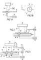
- the part 10 is provided with a circular hole 16 of center O, the hole 16 being linked to this part 10 and constituting the position reference.
- the detection device also includes a camera 17 arranged on the other side of the part 10 with respect to the laser beam 14 and capable to take an image of the periphery of the hole 16 and of the laser beam 14. From this image, a computing circuit 18 associated with the camera allows to calculate the components according to the orthogonal directions X and Y of the segment which joins the center O of the circle and the point of impact A and therefore of completely determine the relative positioning error.
- this device makes it possible to detect and measure two types of absolute positioning error depending on whether the laser beam constitutes the position reference and that the part 10 is mobile or that the part 10 constitutes the position reference by its hole circular 16, the laser beam 14 then being marred by an error possible position.
- the camera 17 must be able to detect the laser beam.
- FIG 2 there is shown the use of the device Figures 1A and 1B to the calibration of the laser beam with respect to the frame an exhibition facility.
- An optical unit 30 has been represented directing a laser beam 32 towards a part 34 integral with the frame 36 of the machine.
- the part 34 is for example constituted by a strip integral with the frame 36 and made of a material of great stability such than Invar.
- the strip 34 is provided with at least two orifices circular 38 and 40 of perfectly defined diameter. Ports 38 and 40 therefore constitute position references of the frame 36.
- the optical unit 30 is associated with a control unit 42 to control the point impact of the laser beam.
- the laser beam to be moved by scanning over a certain distance from the frame we can advantageously repeat the operation in relation to a second reference hole 40 formed in the strip 34 and by controlling the position of the laser beam with instructions corresponding to the position of this second hole 40.
- This error determination can be carried out for several holes arranged on strip 34.
- FIG. 3 we will describe an application of the device for detecting errors relating to the positioning of a printed circuit board 50 in a beam exposure machine laser.
- This panel 50 is provided with two holes for positioning 54 and 56.
- a optical unit 58 which controls the point of impact of a laser beam 60 in response to the instructions transmitted by a control circuit 62.
- the optical unit 58 is controlled so that the beam is focused at a point on the frame corresponding exactly to the position that the center of the positioning hole 54 should occupy.
- the camera 63 we take an image of the periphery of hole 54 and the impact of the laser beam 60 and the coordinates of this error are calculated in the calculation circuit 64.
- the block optic 58 is controlled so that a laser beam 60 'has a point of impact corresponding exactly to the theoretical position of the center of the second positioning hole 56 of the printed circuit board 50.
- a using a second camera 65 we take a second image corresponding to hole 56 and we transmit this second error of position at computation circuit 64.
- Rotation error can be measured by the angle between the straight line joining the centers of holes 54 and 56 and the straight line joining the two impact points of the laser beams.
- the error of rotational position is transmitted to the control circuit 66 actuators 68 to correct this error.
- the errors of position in X and Y are preferably directly transmitted to the circuits 62 of the optical unit 58.
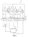
- FIG. 4 shows the case of an exposure machine 70 comprising several laser beams 72 1 , 72 2 , 72 3 , 72 4 produced by as many optical units 74 1 , 74 2 , 74 3 , 74 4 , each optical unit being controlled by a circuit 76.
- the frame 78 of the machine is equipped with an Invar 80 rule comprising as many series S 1 , S 2 , S 3 , S 4 of holes 82 of calibration that there are laser beams to calibrate.
- the holes of a series are respectively arranged opposite the zones Z 1 , Z 2 , Z 3 and Z 4 which the laser beam must scan; each series has for example 20 holes.
Landscapes
- Engineering & Computer Science (AREA)
- Manufacturing & Machinery (AREA)
- Microelectronics & Electronic Packaging (AREA)
- Physics & Mathematics (AREA)
- General Physics & Mathematics (AREA)
- Exposure And Positioning Against Photoresist Photosensitive Materials (AREA)
- Length Measuring Devices By Optical Means (AREA)
- Laser Beam Processing (AREA)
- Body Structure For Vehicles (AREA)
- Length Measuring Devices With Unspecified Measuring Means (AREA)
- Exposure Of Semiconductors, Excluding Electron Or Ion Beam Exposure (AREA)
- Automatic Control Of Machine Tools (AREA)
- Numerical Control (AREA)
Abstract
Description
en ce que ladite pièce est munie d'un orifice circulaire occupant une position de référence par rapport à ladite pièce
et en ce qu'il comprend en outre :
- des moyens pour focaliser le faisceau laser dans le plan de ladite pièce,
- des moyens pour prendre une image dudit trou circulaire et du faisceau focalisé dans le plan de ladite pièce ; et
- des moyens pour calculer les composantes du segment joignant ledit point d'impact et le centre dudit trou.
- des moyens pour focaliser ledit faisceau laser successivement en deux points du bâti correspondant qui devraient être occupés par les centres des deux trous circulaires,
- des moyens par caméra pour prendre une image des deux trous et des points d'impact de faisceau laser,
- des moyens pour calculer à partir de chacune desdites images les composantes du segment joignant le centre du cercle au point d'impact du faisceau par quoi on obtient deux ensembles d'informations d'erreur de position du panneau,
- des moyens pour déplacer ledit panneau par rapport au bâti au moins en rotation, et des moyens pour commander les moyens de déplacement et les moyens de focalisation du faisceau laser en fonction des deux ensembles d'informations d'erreur de position du panneau.
- au moins une pièce solidaire dudit bâti, ladite pièce comportant au moins un trou circulaire dont le centre constitue un point de référence du bâti,
- des moyens pour commander les moyens de déflexion de faisceau par des informations de position correspondant à la position du centre dudit cercle,
- des moyens par caméra pour prendre une image dudit trou circulaire et du point d'impact effectif du faisceau laser dans ledit trou,
- des moyens pour calculer les composantes du segment joignant le centre dudit trou au point d'impact du faisceau laser, et des moyens pour transmettre aux moyens de commande des moyens de déflexion lesdites composantes.
Claims (6)
- Dispositif de mesure d'erreur de position relative entre un faisceau laser et une pièce, caractérisé
en ce que ladite pièce est munie d'un orifice circulaire occupant une position de référence par rapport à ladite pièce
et en ce qu'il comprend en outre :des moyens pour focaliser le faisceau laser dans le plan de ladite pièce,des moyens pour prendre une image dudit trou circulaire et du faisceau focalisé dans le plan de ladite pièce et des moyens pour calculer les composantes du segment joignant ledit point d'impact et le centre dudit trou. - Application du dispositif selon la revendication 1 à la réalisation d'une machine d'exposition de panneaux de circuit imprimé comprenant :caractérisée en ce que ladite machine comprend en outre :un bâti fixe apte à recevoir un panneau de circuit imprimé, ledit panneau étant muni d'au moins deux trous circulaires de positionnement,au moins un laser associé à des moyens optiques pour focaliser le faisceau laser en un point quelconque du circuit imprimé,des moyens pour focaliser ledit faisceau laser successivement en deux points du bâti correspondant qui devraient être occupés par les centres des deux trous circulaires,des moyens par caméra pour prendre une image des deux trous et des points d'impact des faisceaux laser,des moyens pour calculer à partir de chacune desdites images les composantes du segment joignant le centre du cercle au point d'impact du faisceau par quoi on obtient deux ensembles d'informations d'erreur de position du panneau,des moyens pour déplacer ledit panneau par rapport au bâti au moins en rotation, et des moyens pour commander les moyens de déplacement et les moyens de focalisation du faisceau laser en fonction des deux ensembles d'informations d'erreur de position du panneau.
- Application selon la revendication 2, caractérisée en ce que les moyens de calcul déterminent l'angle entre les segments joignant les deux points d'impact des faisceaux laser et les deux centres des trous, ce qui donne une information d'erreur de position en rotation du centre d'un deuxième trou par rapport au centre du premier, et les composantes selon deux directions orthogonales du bâti de l'erreur de position du centre du premier trou, et en ce que les moyens de commande comprennent :des moyens pour commander les moyens de déplacement en rotation en fonction de l'erreur en rotation calculée, etdes moyens pour transmettre aux moyens de focalisation desdits faisceaux laser lesdites composantes.
- Application du dispositif selon la revendication 1 à la réalisation d'une machine d'exposition de panneaux de circuit imprimé comprenant :un bâti fixe pour recevoir ledit panneau,une source laser pour produire au moins un faisceau laser et des moyens de commande de déflexion du faisceau laser, ladite machine étant caractérisée en ce qu'elle comprend en outre :au moins une pièce solidaire dudit bâti, ladite pièce comportant au moins un trou circulaire dont le centre constitue un point de référence du bâti,des moyens pour commander les moyens de déflexion de faisceau par des informations de position correspondant à la position du centre dudit cercle,des moyens par caméra pour prendre une image dudit trou circulaire et du point d'impact effectif du faisceau laser dans ledit trou,des moyens pour calculer les composantes du segment joignant le centre dudit trou au point d'impact du faisceau laser, etdes moyens pour transmettre aux moyens de commande des moyens de déflexion lesdites composantes.
- Application selon la revendication 4, caractérisée en ce que :ladite pièce comporte une série de trous circulaires dont les centres définissent une série de position de référence du bâti,en ce que les moyens de commande comportent des moyens pour commander successivement les moyens de déflexion du faiscau laser par une série d'informations de position correspondant aux positions des centres de la série de trous,en ce que les moyens par caméra prennent successivement une série d'images pour chaque trou,en ce que les moyens de calcul déterminent lesdites composantes pour chaque image de la série d'images et élaborent une fonction polynomiale de correction de position du faisceau laser à partir de ladite série de composantes en fonction de la position des centres de la série de trous ; eten ce que les moyens de transmission transmettent ladite fonction polynomiale de correction auxdits moyens de commande des moyens de déflexion.
- Application selon la revendication 5, caractérisée en ce que
ladite machine comprend :en ce que ladite pièce comporte une pluralité de séries de trous, chaque série de trous correspondant à la portion de circuit imprimé balayée par ledit faisceau laser, etdes moyens pour produire une pluralité de faisceaux laser, etune pluralité de moyens de déflexion, chaque moyen de déflexion étant associé à un faisceau laser ; chaque moyen de déflexion étant associé à un moyen de commande pour que chaque faisceau laser balaie une portion dudit panneau de circuit imprimé,
en ce que lesdits moyens de calcul déterminent une fonction polynomiale de correction de position pour chaque série d'images associée à une série de trous.
Applications Claiming Priority (2)
| Application Number | Priority Date | Filing Date | Title |
|---|---|---|---|
| FR9913725A FR2800565B1 (fr) | 1999-11-03 | 1999-11-03 | Dispositif de mesure d'erreur de position relative |
| FR9913725 | 1999-11-03 |
Publications (2)
| Publication Number | Publication Date |
|---|---|
| EP1098556A1 true EP1098556A1 (fr) | 2001-05-09 |
| EP1098556B1 EP1098556B1 (fr) | 2007-02-07 |
Family
ID=9551646
Family Applications (1)
| Application Number | Title | Priority Date | Filing Date |
|---|---|---|---|
| EP00402847A Expired - Lifetime EP1098556B1 (fr) | 1999-11-03 | 2000-10-16 | Dispositif de mesure d'erreur de position relative |
Country Status (11)
| Country | Link |
|---|---|
| US (1) | US6683684B1 (fr) |
| EP (1) | EP1098556B1 (fr) |
| JP (1) | JP2001188007A (fr) |
| KR (1) | KR20010060196A (fr) |
| CN (1) | CN1220116C (fr) |
| AT (1) | ATE353538T1 (fr) |
| CA (1) | CA2324913A1 (fr) |
| DE (1) | DE60033258T2 (fr) |
| ES (1) | ES2281329T3 (fr) |
| FR (1) | FR2800565B1 (fr) |
| TW (1) | TW556456B (fr) |
Cited By (1)
| Publication number | Priority date | Publication date | Assignee | Title |
|---|---|---|---|---|
| CN102865815A (zh) * | 2012-09-24 | 2013-01-09 | 上海功源电子科技有限公司 | 一种新型的单视觉相机对位pcb的定位补偿方法 |
Families Citing this family (16)
| Publication number | Priority date | Publication date | Assignee | Title |
|---|---|---|---|---|
| KR20050035153A (ko) * | 2001-10-10 | 2005-04-15 | 액센트 옵티칼 테크놀로지스 인코포레이티드 | 단면 분석법에 의한 초점 중심의 결정 |
| JP4338577B2 (ja) * | 2004-04-28 | 2009-10-07 | 株式会社ブイ・テクノロジー | 露光装置 |
| JP4391545B2 (ja) * | 2007-03-30 | 2009-12-24 | 日立ビアメカニクス株式会社 | ワーク加工機 |
| CN101450788B (zh) * | 2007-12-05 | 2011-04-13 | 中国科学院微电子研究所 | 石英晶圆深微孔加工设备及方法 |
| CN104378916B (zh) * | 2013-08-13 | 2018-04-03 | 达观科技有限公司 | 物件校正方法 |
| CN104897070B (zh) * | 2014-03-07 | 2018-04-17 | 达观科技有限公司 | 加工物件基础规格的检测方法 |
| JP6483536B2 (ja) * | 2015-06-05 | 2019-03-13 | 株式会社アドテックエンジニアリング | パターン描画装置及びパターン描画方法 |
| CN105043269B (zh) * | 2015-07-08 | 2017-09-29 | 上海与德通讯技术有限公司 | 一种物体尺寸的测量方法及电子设备 |
| CN106767556B (zh) * | 2016-12-26 | 2023-06-06 | 重庆越发机械制造有限公司 | 高精度变档拨叉同心度检测设备 |
| CN111095111B (zh) * | 2017-09-11 | 2024-12-20 | Asml荷兰有限公司 | 光刻装置和方法 |
| CN109209546B (zh) * | 2018-09-30 | 2019-12-27 | 东风汽车集团有限公司 | 连续可变气门升程机构的间隙调节装置及调节方法 |
| CN112179286B (zh) * | 2020-08-18 | 2021-12-21 | 江苏瑞尔隆盛叶轮科技有限公司 | 一种gom三维光学扫描仪专用夹具 |
| CN111928873A (zh) * | 2020-09-28 | 2020-11-13 | 快克智能装备股份有限公司 | 一种标定测高中心与相机中心的方法 |
| CN112857220B (zh) * | 2021-01-13 | 2022-08-09 | 德阳市产品质量监督检验所 | 一种发电设备零部件的检测结构 |
| CN113207232A (zh) * | 2021-04-30 | 2021-08-03 | 东莞市五株电子科技有限公司 | 一种三维pcb的制作方法及pcb |
| WO2026027926A1 (fr) * | 2024-08-01 | 2026-02-05 | Sevostianov Petr | Dispositif et procédé de fabrication de cartes de circuit imprimé |
Citations (3)
| Publication number | Priority date | Publication date | Assignee | Title |
|---|---|---|---|---|
| DD241562A1 (de) * | 1985-10-10 | 1986-12-17 | Robotron Bueromasch | Messtechnische anordnung zur ueberwachung des schneidvorganges beim lasertrennen |
| EP0618505A1 (fr) * | 1993-03-31 | 1994-10-05 | Automa-Tech | Installation d'exposition à la lumière d'une plaque de circuit imprimé double face à travers des clichés |
| EP0827035A2 (fr) * | 1996-08-26 | 1998-03-04 | Demminer Maschinen Technik GmbH | Méthode et appareil pour aligner des masques photolithographiques dans une ligne de production |
Family Cites Families (2)
| Publication number | Priority date | Publication date | Assignee | Title |
|---|---|---|---|---|
| DE241562C (fr) | 1909-07-31 | 1911-12-05 | ||
| US5264869A (en) * | 1991-08-19 | 1993-11-23 | Xerox Corporation | Electro-optical control apparatus and system for spot position control in an optical output device |
-
1999
- 1999-11-03 FR FR9913725A patent/FR2800565B1/fr not_active Expired - Fee Related
-
2000
- 2000-10-16 AT AT00402847T patent/ATE353538T1/de not_active IP Right Cessation
- 2000-10-16 DE DE60033258T patent/DE60033258T2/de not_active Expired - Fee Related
- 2000-10-16 ES ES00402847T patent/ES2281329T3/es not_active Expired - Lifetime
- 2000-10-16 EP EP00402847A patent/EP1098556B1/fr not_active Expired - Lifetime
- 2000-10-16 US US09/688,900 patent/US6683684B1/en not_active Expired - Fee Related
- 2000-10-23 KR KR1020000062366A patent/KR20010060196A/ko not_active Withdrawn
- 2000-10-31 CA CA002324913A patent/CA2324913A1/fr not_active Abandoned
- 2000-11-02 TW TW089123119A patent/TW556456B/zh not_active IP Right Cessation
- 2000-11-02 JP JP2000336242A patent/JP2001188007A/ja not_active Withdrawn
- 2000-11-03 CN CNB001338080A patent/CN1220116C/zh not_active Expired - Fee Related
Patent Citations (3)
| Publication number | Priority date | Publication date | Assignee | Title |
|---|---|---|---|---|
| DD241562A1 (de) * | 1985-10-10 | 1986-12-17 | Robotron Bueromasch | Messtechnische anordnung zur ueberwachung des schneidvorganges beim lasertrennen |
| EP0618505A1 (fr) * | 1993-03-31 | 1994-10-05 | Automa-Tech | Installation d'exposition à la lumière d'une plaque de circuit imprimé double face à travers des clichés |
| EP0827035A2 (fr) * | 1996-08-26 | 1998-03-04 | Demminer Maschinen Technik GmbH | Méthode et appareil pour aligner des masques photolithographiques dans une ligne de production |
Cited By (2)
| Publication number | Priority date | Publication date | Assignee | Title |
|---|---|---|---|---|
| CN102865815A (zh) * | 2012-09-24 | 2013-01-09 | 上海功源电子科技有限公司 | 一种新型的单视觉相机对位pcb的定位补偿方法 |
| CN102865815B (zh) * | 2012-09-24 | 2015-01-07 | 上海功源电子科技有限公司 | 一种新型的单视觉相机对位pcb的定位补偿方法 |
Also Published As
| Publication number | Publication date |
|---|---|
| JP2001188007A (ja) | 2001-07-10 |
| CN1295268A (zh) | 2001-05-16 |
| CA2324913A1 (fr) | 2001-05-03 |
| DE60033258T2 (de) | 2007-11-22 |
| CN1220116C (zh) | 2005-09-21 |
| EP1098556B1 (fr) | 2007-02-07 |
| FR2800565B1 (fr) | 2002-10-25 |
| ATE353538T1 (de) | 2007-02-15 |
| FR2800565A1 (fr) | 2001-05-04 |
| US6683684B1 (en) | 2004-01-27 |
| TW556456B (en) | 2003-10-01 |
| ES2281329T3 (es) | 2007-10-01 |
| DE60033258D1 (de) | 2007-03-22 |
| KR20010060196A (ko) | 2001-07-06 |
Similar Documents
| Publication | Publication Date | Title |
|---|---|---|
| EP1098556B1 (fr) | Dispositif de mesure d'erreur de position relative | |
| US8675077B2 (en) | Alignment metrology and resolution measurement system for imaging arrays | |
| EP0113633B1 (fr) | Procédé et dispositif d'alignement optique de motifs dans deux plans rapprochés dans un appareil d'exposition comprenant une source de rayonnement divergent | |
| CN102326114B (zh) | 光轴调整装置、光轴调整方法及投射型显示装置 | |
| EP1733181B2 (fr) | Palpeur mixte, optique et mecanique et procede de recalage y afferant | |
| US7692128B2 (en) | Focus control method for an optical apparatus which inspects a photo-mask or the like | |
| FR2916534A1 (fr) | Procede et dispositif pour la mesure sans contact d'oscillations d'un objet | |
| FR2539525A1 (fr) | Procede pour corriger l'intensite d'un faisceau lors de l'analyse et de l'enregistrement d'une figure | |
| FR2534017A1 (fr) | Procede et appareil pour realiser l'alignement statique d'arbres et pour controler cet alignement | |
| US8294902B2 (en) | Measuring method and measuring device for measuring a shape of a measurement surface using a reference standard for calibration | |
| WO2011076844A1 (fr) | Procede d'ablation d'une surface en trois dimensions grace a un dispositif d'ablation laser et grace a l'emploi d'une etape d'etalonnage; dispositif de mise en oeuvre d'un tel procede | |
| FR2858680A1 (fr) | Systeme de plate-forme stabilisee | |
| EP0712009A1 (fr) | Ecartomètre intégré | |
| EP0015789B1 (fr) | Dispositif optique de projection en photorépétition | |
| EP0618505B1 (fr) | Installation d'exposition à la lumière d'une plaque de circuit imprimé double face à travers des clichés | |
| FR2467385A1 (fr) | Appareil et son utilisation en vue de controler l'alignement d'essieux de roues | |
| FR2979023A1 (fr) | Procede de determination de la mise au point et de la dose d'un equipement de micro-lithographie optique | |
| FR2541471A1 (fr) | Element en forme de feuille a aligner sur un autre element presentant une zone dessinee, et appareil et reticule pour l'alignement de ces elements | |
| US20060018560A1 (en) | Exposure device and exposure method | |
| EP0156683B1 (fr) | Appareil de microlithographie optique à système d'alignement local | |
| EP0578562B1 (fr) | Procédé de détermination de la mise au point d'une machine d'exposition photolithographique | |
| FR2841993A1 (fr) | Procede et appareil pour aligner un reseau de diffraction | |
| JP2015219244A (ja) | 基板処理装置、デバイス製造方法及び基板処理方法 | |
| JP2005292103A (ja) | ポリゴンミラーの角度測定装置 | |
| FR2713785A1 (fr) | Système de repérage d'orientation d'un instrument d'observation. |
Legal Events
| Date | Code | Title | Description |
|---|---|---|---|
| PUAI | Public reference made under article 153(3) epc to a published international application that has entered the european phase |
Free format text: ORIGINAL CODE: 0009012 |
|
| AK | Designated contracting states |
Kind code of ref document: A1 Designated state(s): AT BE CH CY DE DK ES FI FR GB GR IE IT LI LU MC NL PT SE |
|
| AX | Request for extension of the european patent |
Free format text: AL;LT;LV;MK;RO;SI |
|
| 17P | Request for examination filed |
Effective date: 20010716 |
|
| AKX | Designation fees paid |
Free format text: AT BE CH CY DE DK ES FI FR GB GR IE IT LI LU MC NL PT SE |
|
| GRAP | Despatch of communication of intention to grant a patent |
Free format text: ORIGINAL CODE: EPIDOSNIGR1 |
|
| GRAS | Grant fee paid |
Free format text: ORIGINAL CODE: EPIDOSNIGR3 |
|
| GRAA | (expected) grant |
Free format text: ORIGINAL CODE: 0009210 |
|
| AK | Designated contracting states |
Kind code of ref document: B1 Designated state(s): AT BE CH CY DE DK ES FI FR GB GR IE IT LI LU MC NL PT SE |
|
| PG25 | Lapsed in a contracting state [announced via postgrant information from national office to epo] |
Ref country code: NL Free format text: LAPSE BECAUSE OF FAILURE TO SUBMIT A TRANSLATION OF THE DESCRIPTION OR TO PAY THE FEE WITHIN THE PRESCRIBED TIME-LIMIT Effective date: 20070207 Ref country code: IE Free format text: LAPSE BECAUSE OF FAILURE TO SUBMIT A TRANSLATION OF THE DESCRIPTION OR TO PAY THE FEE WITHIN THE PRESCRIBED TIME-LIMIT Effective date: 20070207 Ref country code: FI Free format text: LAPSE BECAUSE OF FAILURE TO SUBMIT A TRANSLATION OF THE DESCRIPTION OR TO PAY THE FEE WITHIN THE PRESCRIBED TIME-LIMIT Effective date: 20070207 Ref country code: DK Free format text: LAPSE BECAUSE OF FAILURE TO SUBMIT A TRANSLATION OF THE DESCRIPTION OR TO PAY THE FEE WITHIN THE PRESCRIBED TIME-LIMIT Effective date: 20070207 |
|
| REG | Reference to a national code |
Ref country code: GB Ref legal event code: FG4D Free format text: NOT ENGLISH |
|
| REG | Reference to a national code |
Ref country code: CH Ref legal event code: EP |
|
| REG | Reference to a national code |
Ref country code: IE Ref legal event code: FG4D Free format text: LANGUAGE OF EP DOCUMENT: FRENCH |
|
| REF | Corresponds to: |
Ref document number: 60033258 Country of ref document: DE Date of ref document: 20070322 Kind code of ref document: P |
|
| PG25 | Lapsed in a contracting state [announced via postgrant information from national office to epo] |
Ref country code: SE Free format text: LAPSE BECAUSE OF FAILURE TO SUBMIT A TRANSLATION OF THE DESCRIPTION OR TO PAY THE FEE WITHIN THE PRESCRIBED TIME-LIMIT Effective date: 20070507 |
|
| GBT | Gb: translation of ep patent filed (gb section 77(6)(a)/1977) |
Effective date: 20070413 |
|
| PG25 | Lapsed in a contracting state [announced via postgrant information from national office to epo] |
Ref country code: PT Free format text: LAPSE BECAUSE OF FAILURE TO SUBMIT A TRANSLATION OF THE DESCRIPTION OR TO PAY THE FEE WITHIN THE PRESCRIBED TIME-LIMIT Effective date: 20070709 |
|
| NLV1 | Nl: lapsed or annulled due to failure to fulfill the requirements of art. 29p and 29m of the patents act | ||
| REG | Reference to a national code |
Ref country code: IE Ref legal event code: FD4D |
|
| REG | Reference to a national code |
Ref country code: ES Ref legal event code: FG2A Ref document number: 2281329 Country of ref document: ES Kind code of ref document: T3 |
|
| PLBE | No opposition filed within time limit |
Free format text: ORIGINAL CODE: 0009261 |
|
| STAA | Information on the status of an ep patent application or granted ep patent |
Free format text: STATUS: NO OPPOSITION FILED WITHIN TIME LIMIT |
|
| 26N | No opposition filed |
Effective date: 20071108 |
|
| PGFP | Annual fee paid to national office [announced via postgrant information from national office to epo] |
Ref country code: ES Payment date: 20071017 Year of fee payment: 8 Ref country code: DE Payment date: 20071010 Year of fee payment: 8 |
|
| PGFP | Annual fee paid to national office [announced via postgrant information from national office to epo] |
Ref country code: AT Payment date: 20070917 Year of fee payment: 8 Ref country code: IT Payment date: 20071020 Year of fee payment: 8 |
|
| BERE | Be: lapsed |
Owner name: AUTOMA-TECH Effective date: 20071031 |
|
| PG25 | Lapsed in a contracting state [announced via postgrant information from national office to epo] |
Ref country code: GR Free format text: LAPSE BECAUSE OF FAILURE TO SUBMIT A TRANSLATION OF THE DESCRIPTION OR TO PAY THE FEE WITHIN THE PRESCRIBED TIME-LIMIT Effective date: 20070508 |
|
| PGFP | Annual fee paid to national office [announced via postgrant information from national office to epo] |
Ref country code: GB Payment date: 20071016 Year of fee payment: 8 Ref country code: FR Payment date: 20071026 Year of fee payment: 8 |
|
| PG25 | Lapsed in a contracting state [announced via postgrant information from national office to epo] |
Ref country code: MC Free format text: LAPSE BECAUSE OF NON-PAYMENT OF DUE FEES Effective date: 20071031 |
|
| REG | Reference to a national code |
Ref country code: CH Ref legal event code: PL |
|
| PG25 | Lapsed in a contracting state [announced via postgrant information from national office to epo] |
Ref country code: LI Free format text: LAPSE BECAUSE OF NON-PAYMENT OF DUE FEES Effective date: 20071031 Ref country code: CH Free format text: LAPSE BECAUSE OF NON-PAYMENT OF DUE FEES Effective date: 20071031 |
|
| PG25 | Lapsed in a contracting state [announced via postgrant information from national office to epo] |
Ref country code: BE Free format text: LAPSE BECAUSE OF NON-PAYMENT OF DUE FEES Effective date: 20071031 |
|
| GBPC | Gb: european patent ceased through non-payment of renewal fee |
Effective date: 20081016 |
|
| REG | Reference to a national code |
Ref country code: FR Ref legal event code: ST Effective date: 20090630 |
|
| PG25 | Lapsed in a contracting state [announced via postgrant information from national office to epo] |
Ref country code: CY Free format text: LAPSE BECAUSE OF FAILURE TO SUBMIT A TRANSLATION OF THE DESCRIPTION OR TO PAY THE FEE WITHIN THE PRESCRIBED TIME-LIMIT Effective date: 20070207 |
|
| PG25 | Lapsed in a contracting state [announced via postgrant information from national office to epo] |
Ref country code: LU Free format text: LAPSE BECAUSE OF NON-PAYMENT OF DUE FEES Effective date: 20071016 Ref country code: IT Free format text: LAPSE BECAUSE OF NON-PAYMENT OF DUE FEES Effective date: 20081016 Ref country code: DE Free format text: LAPSE BECAUSE OF NON-PAYMENT OF DUE FEES Effective date: 20090501 Ref country code: AT Free format text: LAPSE BECAUSE OF NON-PAYMENT OF DUE FEES Effective date: 20081016 |
|
| PG25 | Lapsed in a contracting state [announced via postgrant information from national office to epo] |
Ref country code: FR Free format text: LAPSE BECAUSE OF NON-PAYMENT OF DUE FEES Effective date: 20081031 |
|
| PG25 | Lapsed in a contracting state [announced via postgrant information from national office to epo] |
Ref country code: GB Free format text: LAPSE BECAUSE OF NON-PAYMENT OF DUE FEES Effective date: 20081016 |
|
| REG | Reference to a national code |
Ref country code: ES Ref legal event code: FD2A Effective date: 20081017 |
|
| PG25 | Lapsed in a contracting state [announced via postgrant information from national office to epo] |
Ref country code: ES Free format text: LAPSE BECAUSE OF NON-PAYMENT OF DUE FEES Effective date: 20081017 |