EP1100193A2 - Circuit de filtrage intégré avec adaptation d'impédance d'entrée et sortie amélioré et procédé de fabrication - Google Patents
Circuit de filtrage intégré avec adaptation d'impédance d'entrée et sortie amélioré et procédé de fabrication Download PDFInfo
- Publication number
- EP1100193A2 EP1100193A2 EP00123638A EP00123638A EP1100193A2 EP 1100193 A2 EP1100193 A2 EP 1100193A2 EP 00123638 A EP00123638 A EP 00123638A EP 00123638 A EP00123638 A EP 00123638A EP 1100193 A2 EP1100193 A2 EP 1100193A2
- Authority
- EP
- European Patent Office
- Prior art keywords
- input
- output
- integrated filter
- integrated
- parasitic shunt
- Prior art date
- Legal status (The legal status is an assumption and is not a legal conclusion. Google has not performed a legal analysis and makes no representation as to the accuracy of the status listed.)
- Withdrawn
Links
- 238000004519 manufacturing process Methods 0.000 title claims abstract description 7
- 230000003071 parasitic effect Effects 0.000 claims abstract description 63
- 230000001939 inductive effect Effects 0.000 claims abstract description 33
- 239000000919 ceramic Substances 0.000 claims abstract description 11
- 230000005540 biological transmission Effects 0.000 claims abstract description 10
- 239000003990 capacitor Substances 0.000 claims description 6
- 238000010897 surface acoustic wave method Methods 0.000 claims description 5
- 230000008878 coupling Effects 0.000 abstract description 16
- 238000010168 coupling process Methods 0.000 abstract description 16
- 238000005859 coupling reaction Methods 0.000 abstract description 16
- 239000011229 interlayer Substances 0.000 abstract 1
- 238000013461 design Methods 0.000 description 10
- 238000000034 method Methods 0.000 description 10
- 238000010586 diagram Methods 0.000 description 7
- 230000002411 adverse Effects 0.000 description 4
- 239000002184 metal Substances 0.000 description 3
- 238000002955 isolation Methods 0.000 description 2
- 238000012986 modification Methods 0.000 description 2
- 230000004048 modification Effects 0.000 description 2
- 238000000926 separation method Methods 0.000 description 2
- 238000013459 approach Methods 0.000 description 1
- 230000001066 destructive effect Effects 0.000 description 1
- 230000000694 effects Effects 0.000 description 1
- 238000010348 incorporation Methods 0.000 description 1
- 230000010354 integration Effects 0.000 description 1
Images


Classifications
-
- H—ELECTRICITY
- H03—ELECTRONIC CIRCUITRY
- H03H—IMPEDANCE NETWORKS, e.g. RESONANT CIRCUITS; RESONATORS
- H03H7/00—Multiple-port networks comprising only passive electrical elements as network components
- H03H7/38—Impedance-matching networks
-
- H—ELECTRICITY
- H03—ELECTRONIC CIRCUITRY
- H03H—IMPEDANCE NETWORKS, e.g. RESONANT CIRCUITS; RESONATORS
- H03H9/00—Networks comprising electromechanical or electro-acoustic elements; Electromechanical resonators
- H03H9/0004—Impedance-matching networks
-
- H—ELECTRICITY
- H03—ELECTRONIC CIRCUITRY
- H03H—IMPEDANCE NETWORKS, e.g. RESONANT CIRCUITS; RESONATORS
- H03H7/00—Multiple-port networks comprising only passive electrical elements as network components
- H03H7/01—Frequency selective two-port networks
-
- H—ELECTRICITY
- H03—ELECTRONIC CIRCUITRY
- H03H—IMPEDANCE NETWORKS, e.g. RESONANT CIRCUITS; RESONATORS
- H03H7/00—Multiple-port networks comprising only passive electrical elements as network components
- H03H7/01—Frequency selective two-port networks
- H03H7/17—Structural details of sub-circuits of frequency selective networks
- H03H7/1741—Comprising typical LC combinations, irrespective of presence and location of additional resistors
- H03H7/1758—Series LC in shunt or branch path
-
- H—ELECTRICITY
- H03—ELECTRONIC CIRCUITRY
- H03H—IMPEDANCE NETWORKS, e.g. RESONANT CIRCUITS; RESONATORS
- H03H7/00—Multiple-port networks comprising only passive electrical elements as network components
- H03H7/01—Frequency selective two-port networks
- H03H7/17—Structural details of sub-circuits of frequency selective networks
- H03H7/1741—Comprising typical LC combinations, irrespective of presence and location of additional resistors
- H03H7/1775—Parallel LC in shunt or branch path
-
- H—ELECTRICITY
- H03—ELECTRONIC CIRCUITRY
- H03H—IMPEDANCE NETWORKS, e.g. RESONANT CIRCUITS; RESONATORS
- H03H7/00—Multiple-port networks comprising only passive electrical elements as network components
- H03H7/38—Impedance-matching networks
- H03H7/383—Impedance-matching networks comprising distributed impedance elements together with lumped impedance elements
-
- H—ELECTRICITY
- H03—ELECTRONIC CIRCUITRY
- H03H—IMPEDANCE NETWORKS, e.g. RESONANT CIRCUITS; RESONATORS
- H03H9/00—Networks comprising electromechanical or electro-acoustic elements; Electromechanical resonators
- H03H9/02—Details
- H03H9/05—Holders or supports
- H03H9/0538—Constructional combinations of supports or holders with electromechanical or other electronic elements
- H03H9/0542—Constructional combinations of supports or holders with electromechanical or other electronic elements consisting of a lateral arrangement
Definitions
- This invention relates to very compact integrated circuits and particularly to integrated filters.
- a frequency selecting filter serves three important functions. namely, passing electrical signals at a desired frequency, rejecting other frequencies, and matching both source and load impedances.
- the ongoing trend of miniaturization through integration presents a problem in filter matching circuit design, in which parasitic shunt capacitance prevents the filter from being matched to its source and load, and also presents a problem in filter stopband isolation design, in which the coupling between the filter's input and output (I/O) sections compromises the filter's stopband rejection performance.
- the parasitic shunt capacitance is small, and its effect on the matching circuit performance is mostly negligible. Also, in conventional filter design, the coupling between a filters I/O sections can be reduced by physically separating these two sections so that the impact on the filter's stopband rejection performance is negligibly small.
- MCIC multilayer ceramic integrated circuits
- MPCB multulayer printed circuit boards
- HDI high density interconnects
- the parasitic shunt capacitance adversely affects the matching circuit performance. This is a relatively new and challenging problem in modern integrated filter design, and the prior art approach, which is to increase spacing between filter elements and to use ground planes, is not a viable solution in integrated filter design.
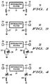
- Circuit 10 includes an integrated filter 11 having an input terminal 12 with input parasitic shunt impedance (not shown) and an output terminal 13 with output parasitic shunt impedance (not shown).
- Integrated filter 11 is any of the modern highly integrated filters, such as those constructed in accordance with the techniques of multilayer ceramic integrated circuits (MCIC), multulayer printed circuit boards (MPCB) and high density interconnects (HDI), etc., in which the input and output parasitic shunt impedances are inherent and adversely affect the matching circuit performance.
- MCIC multilayer ceramic integrated circuits
- MPCB multulayer printed circuit boards
- HDI high density interconnects
- the input and output parasitic shunt impedances are generally distributed shunt capacitances, but can be either a capacitance, an inductance, a resistance, or any combination of the three, and which appear as a lump or discrete component at the specific terminal.
- integrated filter 11 is illustrated in this specific embodiment in a simple block form for convenience.
- Input circuit 14 has a specific impedance, hereinafter referred to as the source impedance.
- Output circuit 15 has a specific impedance, hereinafter referred to as the load impedance.
- Input and output parasitic shunt impedances of filter circuit 10 affect the input and output impedances of filter circuit 10.
- input circuit 14, filter circuit 10, and output circuit 15 operate most efficiently when the source impedance of input circuit 14 matches the input impedance of filter circuit 10 and the output impedance of filter circuit 10 matches the load impedance of output circuit 15.
- filter circuit 10 is fabricated in accordance with the techniques of multilayer ceramic integrated circuits (MCIC), multulayer printed circuit boards (MPCB) and high density interconnects (HDI), etc.
- MCIC multilayer ceramic integrated circuits
- MPCB multulayer printed circuit boards
- HDI high density interconnects
- An input electrical component which in this specific embodiment is an inductive coil 17, has one end connected to input terminal 12 of filter 11 and the other end connected to a common potential, such as ground.
- Inductive coil 17 is, basically, connected in parallel with the input parasitic shunt impedance so as to reduce the input parasitic shunt impedance.
- an output electrical component which in this specific embodiment is an inductive coil 19, has one end connected to output terminal 13 of filter 11 and the other end connected to a common potential, such as ground.
- Inductive coil 19 is, basically, connected in parallel with the output parasitic shunt impedance so as to reduce the output parasitic shunt impedance.
- inductive coils 17 and 19 are most efficient at reducing or canceling input parasitic shunt capacitance and will generally be used in intergated filter circuits in which the input parasitic shunt impedance is a capacitance. Further, input and output inductive coils 17 and 19 can be conveniently integrated into integrated filter circuit 10 as, for example, integrated inductive coils formed in the multilayer ceramic integrated circuit (MCIC), multulayer printed circuit board (MPCB) and high density interconnects (HDI), etc.
- MCIC multilayer ceramic integrated circuit
- MPCB multulayer printed circuit board
- HDI high density interconnects
- Circuit 20 includes an integrated filter 21 having an input terminal 22 with input parasitic shunt impedance (not shown) and an output terminal 23 with output parasitic shunt impedance (not shown).
- integrated filter 21 is any of the modern highly integrated filters, in which the input and output parasitic shunt impedances are inherent and adversely affect the matching circuit performance and the input and output parasitic shunt impedances are either a capacitance, an inductance, a resistance, or any combination of the three, and which appear as a lump or discrete component at the specific terminal.
- integrated filter 21, along with an input circuit 24 and an output circuit 25, are illustrated in this specific embodiment in a simple block form for convenience.
- An input electrical component which in this specific embodiment is a transmission line element 27, has one end connected to input terminal 22 of filter 21 and the other end connected to a common potential, such as ground.
- Transmission line element 27 is, basically, connected in parallel with the input parasitic shunt impedance so as to reduce the input parasitic shunt impedance.
- an output electrical component which in this specific embodiment is a transmission line element 29, has one end connected to output terminal 23 of filter 21 and the other end connected to a common potential, such as ground.
- Transmission line element 29 is, basically, connected in parallel with the output parasitic shunt impedance so as to reduce the output parasitic shunt impedance.
- transmission line elements 27 and 29 can be specifically designed with a length which produces inductive or capacitive impedance to reduce or cancel input parasitic shunt inductance and/or capacitance and will generally be used in intergated filter circuits in which the input parasitic shunt impedance is a capacitance or an inductance. Further, input and output transmission line elements 27 and 29 can be conveniently integrated into integrated filter circuit 20 as, for example, by forming in the multilayer ceramic integrated circuit (MCIC), multulayer printed circuit board (MPCB) and high density interconnects (HDI), etc.
- MCIC multilayer ceramic integrated circuit
- MPCB multulayer printed circuit board
- HDI high density interconnects
- Circuit 30 includes an integrated filter 31 having an input terminal 32 with input parasitic shunt impedance (not shown) and an output terminal 33 with output parasitic shunt impedance (not shown).
- integrated filter 31 is any of the modern highly integrated filters, in which the input and output parasitic shunt impedances are inherent and adversely affect the matching circuit performance and the input and output parasitic shunt impedances are either a capacitance, an inductance, a resistance, or any combination of the three, and which appear as a lump or discrete component at the specific terminal.
- integrated filter 31, along with an input circuit 34 and an output circuit 35, are illustrated in this specific embodiment in a simple block form for convenience.
- An input electrical component which in this specific embodiment is a parallel tuned circuit including a variable capacitance 36 and an inductive coil 37, has one end connected to input terminal 32 of filter 31 and the other end connected to a common potential, such as ground.
- the parallel tuned circuit is, basically, connected in parallel with the input parasitic shunt impedance so as to reduce the input parasitic shunt impedance.
- an output electrical component which in this specific embodiment is a parallel tuned circuit including a variable capacitance 38 and an inductive coil 39, has one end connected to output terminal 33 of filter 31 and the other end connected to a common potential, such as ground.
- the parallel tuned circuit is, basically, connected in parallel with the output parasitic shunt impedance so as to reduce the output parasitic shunt impedance.
- Circuit 40 includes an integrated filter 41 having an input terminal 42 with input parasitic shunt impedance (not shown) and an output terminal 43 with output parasitic shunt impedance (not shown).
- An input electrical component which in this specific embodiment is a series tuned circuit including a variable capacitance 46 and an inductive coil 47, has one end connected to input terminal 42 of filter 41 and the other end connected to a common potential, such as ground.
- an output electrical component which in this specific embodiment is a series tuned circuit including a variable capacitance 48 and an inductive coil 49, has one end connected to output terminal 43 of filter 41 and the other end connected to a common potential, such as ground.
- the input and output series tuned circuits are, basically, connected in parallel with the input and output parasitic shunt impedances, respectively, so as to reduce the output parasitic shunt impedance.
- the input and output parallel and series tuned circuits could be tuned by varying either or both of the capacitances and the inductive coils.
- a variable capacitor since electronic devices such as varactors or voltage variable capacitors (VVC) can be used as the variable capacitors and are easy to integrate into the circuit.
- varactors or VVCs can be tuned or varied by simply applying an appropriate voltage thereto.
- the parallel and series tuned circuits can be tuned to reduce the input and output parasitic shunt impedances, whether inductive, capacitive, and/or resistive and, consequently, offer more design flexibility which leads to better performance.
- FIG. 5 a schematic diagram is illustrated of a tunable transmit integrated filter circuit 50 of a duplexer, implemented in multilayer ceramic integrated circuit (MCIC), in accordance with the present invention.
- Filter circuit 50 includes an integrated filter, generally designated 51, including four series connected sections 52, 53, 54, and 55. Each section 52 through 55 includes a surface acoustic wave (SAW) resonator 56, a voltage variable capacitor 57, and an inductive coil 58 formed in the multilayer ceramics.
- Integrated filter 51 is implemented in MCIC for performance, size, and cost considerations. However, due to the compact implementation, the coupling between the I/Os of adjacent filter sections is inevitable, and this coupling can be capacitive, inductive, or both. Further, the stopband rejection of filter 51 suffers significantly for only very little coupling, e.g. 0.1 pF (capacitance) and 1.0 nH (inductance).
- SAW resonators 56 are capacitively coupled with capacitances 61, 62, and 63. Stray or parasitic capacitances may occur as 60 through 64 and are illustrated as a lump component. Generally, intersection parasitic capacitances 61, 62, and 63 can be absorbed into the design of integrated filter 51, but input parasitic capacitance 60 and output parasitic capacitance 64 cannot be absorbed into the design. Input parasitic capacitance 60 and output parasitic capacitance 64 are each about 0.5 pF and result in a return loss to integrated filter 51 of only 7 dB at the beginning of the passband. This performance is clearly not acceptable.
- An input electrical component 65 which in this specific embodiment is an inductive coil but which may be any one of an inductive coil, a section of transmission line, a series tuned circuit, and a parallel tuned circuit, has one end connected to an input terminal 66 of filter circuit 50 and the other end connected to a common potential, such as ground.
- an output electrical component 67 which in this specific embodiment is an inductive coil but which may be an one of an inductive coil, a section of transmission line, a series tuned circuit, and a parallel tuned circuit, has one end connected to an output terminal 68 of filter circuit 50 and the other end connected to a common potential, such as ground.
- the input and output electrical components 65 and 67 are connected in parallel with the input and output parasitic shunt capacitances 60 and 64, respectively, so as to reduce the input and output parasitic shunt capacitances.
- the return loss of filter circuit 50 is improved to at least 16 dB within the passband.
- additional electrical components similar to those described above, can be used to reduce parasitic shunt capacitances (or other parasitic shunt elements).
- FIG. 6 a layout of the tunable transmit integrated filter circuit of FIG. 5 is illustrated.
- input and output electrical components 65 and 67 which in this specific embodiment are input and output inductive coils, can be physically separated only by an allowable distance, i.e. the width of the MCIC package.
- an allowable distance i.e. the width of the MCIC package.
- the maximum allowable physical separation illustrated in FIG. 6 still provides coupling between input and output electrical components 65 and 67, which results in the stopband rejection of filter circuit 50 being only 26 dB, which is by no means acceptable.
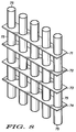
- FIG. 7 a layout is illustrated of the tunable transmit integrated filter circuit of FIG. 5 in accordance with the present invention.
- input and output electrical components 65 and 67 in this specific embodiment are input and output inductive coils, which are hereafter designated 65 and 67, respectively.
- Two different methods and apparatus are used in the structure of FIG. 7 to provide the amount of decoupling required between input and output inductive coils 65 and 67. While these two methods and apparatus are explained separately for convenience in understanding, it should be understood that they may be used separately or together as needed in each application.
- the magnetic fields of input and output inductive coils 65 and 67 can be arranged to create either a constructive or a destructive coupling.
- the capacitive coupling can be thus adjusted to cancel the inductive coupling at stopband frequencies with a net result of a virtual ground between input and output inductive coils 65 and 67.
- This adjustment is substantially different than physically spacing the coils to reduce any kind of coupling and can result in the coils being significantly closer together. Much improved stopband performance can be obtained using this method.
- input and output inductive coils 65 and 67 are positioned substantially adjacent each other and a gridded ground wall 70 is positioned therebetween.
- Gridded ground wall 70 is formed in the MCIC package and is attached to a common potential, such as ground, so as to substantially stop electromagnetic coupling between input and output inductive coils 65 and 67.
- a printed metal trace 71, 72, 73, 74, etc. is formed on each layer of the MCIC or MPCB and vias 75 are formed as interconnections.
- the printed metal traces 71, 72, 73, 74, etc. are connected directly to ground and vias 75 connect all of the remaining printed metal traces to ground.
- the traces and vias or posts provide a grid or gridded wall that is specifically designed to stop electromagnetic coupling.
- the openings in the gridded wall are less than approximately 1/20th of a wavelength of the operating frequency.
- a stopband rejection of 46 dB was achieved.
- the integrated filter circuit includes electrical components for cancelling parasitic shunt impedances so that filter performance is greatly improved. Further,coupling between the filter's input and output sections compromises the filter's stopband rejection performance.
- Two different methods and apparatus are described to improve a filter's stopband isolation, which methods and apparatus include either electrically isolating the filter's I/O sections with a gridded ground wall or electromagnetically cancelling the coupling between the I/O sections. In specific applications it may be possible or convenient to provided limited embodiments of both.
Landscapes
- Physics & Mathematics (AREA)
- Acoustics & Sound (AREA)
- Surface Acoustic Wave Elements And Circuit Networks Thereof (AREA)
- Filters And Equalizers (AREA)
Applications Claiming Priority (2)
| Application Number | Priority Date | Filing Date | Title |
|---|---|---|---|
| US436428 | 1999-11-09 | ||
| US09/436,428 US6426683B1 (en) | 1999-11-09 | 1999-11-09 | Integrated filter with improved I/O matching and method of fabrication |
Publications (2)
| Publication Number | Publication Date |
|---|---|
| EP1100193A2 true EP1100193A2 (fr) | 2001-05-16 |
| EP1100193A3 EP1100193A3 (fr) | 2008-01-23 |
Family
ID=23732360
Family Applications (1)
| Application Number | Title | Priority Date | Filing Date |
|---|---|---|---|
| EP00123638A Withdrawn EP1100193A3 (fr) | 1999-11-09 | 2000-10-30 | Circuit de filtrage intégré avec adaptation d'impédance d'entrée et sortie amélioré et procédé de fabrication |
Country Status (5)
| Country | Link |
|---|---|
| US (1) | US6426683B1 (fr) |
| EP (1) | EP1100193A3 (fr) |
| JP (1) | JP4700184B2 (fr) |
| KR (1) | KR100652546B1 (fr) |
| CN (1) | CN1167197C (fr) |
Cited By (5)
| Publication number | Priority date | Publication date | Assignee | Title |
|---|---|---|---|---|
| EP1536558A1 (fr) * | 2003-11-28 | 2005-06-01 | TDK Corporation | Symétriseur |
| EP1703582A1 (fr) * | 2005-03-16 | 2006-09-20 | TDK Corporation | Symétriseur compacte |
| WO2011147469A1 (fr) * | 2010-05-28 | 2011-12-01 | Verigy (Singapore) Pte. Ltd. | Structure de filtre électrique |
| CN102823129A (zh) * | 2010-01-15 | 2012-12-12 | 维斯普瑞公司 | 可调匹配网路电路拓扑装置及方法 |
| US9203371B2 (en) | 2010-05-28 | 2015-12-01 | Advantest Corporation | Electrical double filter structure |
Families Citing this family (19)
| Publication number | Priority date | Publication date | Assignee | Title |
|---|---|---|---|---|
| US6914493B2 (en) * | 2001-03-08 | 2005-07-05 | Rf Monolithics, Inc. | Noise resistant low phase noise, frequency tracking oscillators and methods of operating the same |
| US6909334B2 (en) * | 2001-03-08 | 2005-06-21 | Rf Monolithics, Inc. | Low phase noise, wide tune range saw oscillators and methods of operating the same |
| US6924716B2 (en) * | 2003-07-10 | 2005-08-02 | Motorola, Inc. | Method and apparatus for reduction of electromagnetic feed through in a SAW filter |
| US7030717B2 (en) * | 2004-05-19 | 2006-04-18 | Soontai Tech Co., Ltd | Impedance-matching wave filter |
| US7421252B2 (en) * | 2005-08-02 | 2008-09-02 | Freescale Semiconductor, Inc. | Center frequency control of an integrated phase rotator band-pass filter using VCO coarse trim bits |
| US8039880B2 (en) * | 2005-09-13 | 2011-10-18 | Raytheon Company | High performance microwave switching devices and circuits |
| DE102005051852B4 (de) * | 2005-10-28 | 2021-05-20 | Snaptrack, Inc. | SAW Filter mit breitbandiger Bandsperre |
| JP2007201350A (ja) | 2006-01-30 | 2007-08-09 | Sanyo Electric Co Ltd | 半導体集積回路 |
| CN101501991B (zh) * | 2006-06-27 | 2012-06-13 | 传感电子公司 | 带有动态阻抗匹配的谐振电路调谐系统 |
| US7579670B2 (en) * | 2006-07-03 | 2009-08-25 | Semiconductor Components Industries, L.L.C. | Integrated filter having ground plane structure |
| KR100792132B1 (ko) * | 2007-06-18 | 2008-01-04 | 이영숙 | 체인형 아이젠 |
| US8405467B2 (en) * | 2007-11-27 | 2013-03-26 | Qualcomm Incorporated | Methods and apparatuses for inductor tuning in radio frequency integrated circuits |
| US8131247B2 (en) * | 2009-05-20 | 2012-03-06 | Broadcom Corporation | Method and system for an intermediate frequency (IF) channel select filter with an integrated alternate adjacent channel interference (AACI) filter |
| US9209772B2 (en) * | 2010-05-28 | 2015-12-08 | Advantest Corporation | Electrical filter structure |
| DE102013104842B4 (de) | 2013-05-10 | 2015-11-12 | Epcos Ag | Zur Miniaturisierung geeignetes HF-Bauelement mit verringerter Kopplung |
| CN105594123B (zh) * | 2013-09-26 | 2019-03-12 | 株式会社村田制作所 | 可变频滤波器 |
| DE102014102707A1 (de) * | 2014-02-28 | 2015-09-03 | Epcos Ag | Abstimmbares elektroakustisches HF-Filter mit verbesserten elektrischen Eigenschaften und Verfahren zum Betrieb eines solchen Filters |
| CN105048988B (zh) * | 2015-07-01 | 2017-11-07 | 东南大学 | 氮化镓基低漏电流固支梁的开关电容滤波器及制备方法 |
| DE102019101888B4 (de) * | 2019-01-25 | 2020-10-08 | RF360 Europe GmbH | Konfigurierbares mikroakustisches HF-Filter |
Citations (1)
| Publication number | Priority date | Publication date | Assignee | Title |
|---|---|---|---|---|
| JPH0998056A (ja) | 1995-09-29 | 1997-04-08 | Toshiba Corp | 弾性表面波装置 |
Family Cites Families (11)
| Publication number | Priority date | Publication date | Assignee | Title |
|---|---|---|---|---|
| US3812442A (en) * | 1972-02-29 | 1974-05-21 | W Muckelroy | Ceramic inductor |
| JPS57194615A (en) * | 1981-05-27 | 1982-11-30 | Clarion Co Ltd | Matching circuit for surface acoustic wave |
| JPH02237211A (ja) * | 1989-03-10 | 1990-09-19 | Nec Corp | 弾性表面波フィルタ |
| JPH03165058A (ja) * | 1989-11-24 | 1991-07-17 | Mitsubishi Electric Corp | 半導体装置 |
| JP3532624B2 (ja) * | 1993-10-08 | 2004-05-31 | 松下電器産業株式会社 | 弾性表面波フィルタ |
| DE69424737T2 (de) * | 1993-10-08 | 2000-09-28 | Matsushita Electric Ind Co Ltd | Akustisches Oberflächenwellenfilter |
| US5457427A (en) * | 1994-04-29 | 1995-10-10 | Philips Electronics North America Corporation | High-frequency amplifier means with enhanced output resistance |
| NO301202B1 (no) * | 1995-06-28 | 1997-09-22 | Ame Space As | Tilpasningskrets |
| JPH09121138A (ja) * | 1995-08-24 | 1997-05-06 | Fujitsu Ltd | フィルタ装置及びこれを用いた無線装置 |
| JPH10209374A (ja) * | 1997-01-21 | 1998-08-07 | Murata Mfg Co Ltd | 集積化デバイス |
| US5933062A (en) * | 1997-11-04 | 1999-08-03 | Motorola Inc. | Acoustic wave ladder filter with effectively increased coupling coefficient and method of providing same |
-
1999
- 1999-11-09 US US09/436,428 patent/US6426683B1/en not_active Expired - Lifetime
-
2000
- 2000-10-19 KR KR1020000061462A patent/KR100652546B1/ko not_active Expired - Fee Related
- 2000-10-30 JP JP2000330019A patent/JP4700184B2/ja not_active Expired - Lifetime
- 2000-10-30 EP EP00123638A patent/EP1100193A3/fr not_active Withdrawn
- 2000-11-08 CN CNB001329383A patent/CN1167197C/zh not_active Expired - Fee Related
Patent Citations (1)
| Publication number | Priority date | Publication date | Assignee | Title |
|---|---|---|---|---|
| JPH0998056A (ja) | 1995-09-29 | 1997-04-08 | Toshiba Corp | 弾性表面波装置 |
Cited By (12)
| Publication number | Priority date | Publication date | Assignee | Title |
|---|---|---|---|---|
| EP1536558A1 (fr) * | 2003-11-28 | 2005-06-01 | TDK Corporation | Symétriseur |
| US7116185B2 (en) | 2003-11-28 | 2006-10-03 | Tdk Corporation | Balun |
| EP1703582A1 (fr) * | 2005-03-16 | 2006-09-20 | TDK Corporation | Symétriseur compacte |
| US7250828B2 (en) | 2005-03-16 | 2007-07-31 | Tdk Corporation | Compact balun |
| CN102823129A (zh) * | 2010-01-15 | 2012-12-12 | 维斯普瑞公司 | 可调匹配网路电路拓扑装置及方法 |
| EP2524428A4 (fr) * | 2010-01-15 | 2013-08-21 | Wispry Inc | Dispositifs et procédés de topologie de circuit de réseau d'adaptation accordable |
| US8680940B2 (en) | 2010-01-15 | 2014-03-25 | Wispry, Inc. | Tunable matching network circuit topology devices and methods |
| CN102823129B (zh) * | 2010-01-15 | 2015-07-08 | 维斯普瑞公司 | 可调匹配网路电路拓扑装置及方法 |
| EP2524428B1 (fr) * | 2010-01-15 | 2018-03-21 | Wispry, Inc. | Dispositifs et procédés de topologie de circuit de réseau d'adaptation accordable |
| WO2011147469A1 (fr) * | 2010-05-28 | 2011-12-01 | Verigy (Singapore) Pte. Ltd. | Structure de filtre électrique |
| KR101441343B1 (ko) * | 2010-05-28 | 2014-09-18 | 어드밴테스트 (싱가포르) 피티이. 엘티디. | 전기 필터 구조 |
| US9203371B2 (en) | 2010-05-28 | 2015-12-01 | Advantest Corporation | Electrical double filter structure |
Also Published As
| Publication number | Publication date |
|---|---|
| KR100652546B1 (ko) | 2006-12-01 |
| CN1295379A (zh) | 2001-05-16 |
| CN1167197C (zh) | 2004-09-15 |
| JP4700184B2 (ja) | 2011-06-15 |
| EP1100193A3 (fr) | 2008-01-23 |
| US6426683B1 (en) | 2002-07-30 |
| KR20010051114A (ko) | 2001-06-25 |
| JP2001185990A (ja) | 2001-07-06 |
Similar Documents
| Publication | Publication Date | Title |
|---|---|---|
| US6426683B1 (en) | Integrated filter with improved I/O matching and method of fabrication | |
| EP1354502B1 (fr) | Traversee de carte de circuit imprime haute frequence | |
| US5039965A (en) | Radio frequency filter feedthrough structure for multilayer circuit boards | |
| JP4579198B2 (ja) | 多層帯域通過フィルタ | |
| JP4925185B2 (ja) | ノイズフィルタアレイ | |
| US20020057139A1 (en) | Monolithic LC components | |
| EP1265311B1 (fr) | Filtre stratifié, dispositif intégré et appareil de communication | |
| US20090033439A1 (en) | Multilayer filter | |
| US7443268B2 (en) | Bandpass filter within a multilayered low temperature co-fired ceramic substrate | |
| US9413324B2 (en) | Electronic component | |
| US6492886B1 (en) | Laminated filter, duplexer, and mobile communication apparatus using the same | |
| KR100744203B1 (ko) | 수동 부품 | |
| CN108432133A (zh) | 高频模块 | |
| JP2004320561A (ja) | 受動部品 | |
| US20030085780A1 (en) | Asymmetric high frequency filtering apparatus | |
| US6335663B1 (en) | Multiplexer/branching filter | |
| US10560069B2 (en) | Elastic wave apparatus | |
| JPH0685506A (ja) | デュプレクサ | |
| CN101485084A (zh) | 平面基板上滤波器的接地策略 | |
| US7800465B2 (en) | Passive component | |
| US20050046512A1 (en) | Demultiplexer | |
| US20070188273A1 (en) | Resonant circuit, filter circuit, and multilayered substrate | |
| JP2004320556A (ja) | 受動部品 | |
| JP5007499B2 (ja) | ノイズフィルタアレイ | |
| JP2008061082A (ja) | バランスフィルタ回路及びこれを用いた高周波装置 |
Legal Events
| Date | Code | Title | Description |
|---|---|---|---|
| PUAI | Public reference made under article 153(3) epc to a published international application that has entered the european phase |
Free format text: ORIGINAL CODE: 0009012 |
|
| AK | Designated contracting states |
Kind code of ref document: A2 Designated state(s): AT BE CH CY DE DK ES FI FR GB GR IE IT LI LU MC NL PT SE |
|
| AX | Request for extension of the european patent |
Free format text: AL;LT;LV;MK;RO;SI |
|
| RAP1 | Party data changed (applicant data changed or rights of an application transferred) |
Owner name: FREESCALE SEMICONDUCTOR, INC. |
|
| PUAL | Search report despatched |
Free format text: ORIGINAL CODE: 0009013 |
|
| AK | Designated contracting states |
Kind code of ref document: A3 Designated state(s): AT BE CH CY DE DK ES FI FR GB GR IE IT LI LU MC NL PT SE |
|
| AX | Request for extension of the european patent |
Extension state: AL LT LV MK RO SI |
|
| RIC1 | Information provided on ipc code assigned before grant |
Ipc: H03H 7/38 20060101ALI20071214BHEP Ipc: H03H 9/00 20060101ALI20071214BHEP Ipc: H03H 9/145 20060101ALI20071214BHEP Ipc: H03H 7/01 20060101AFI20010226BHEP |
|
| 17P | Request for examination filed |
Effective date: 20080723 |
|
| AKX | Designation fees paid |
Designated state(s): AT BE CH CY DE DK ES FI FR GB GR IE IT LI LU MC NL PT SE |
|
| 17Q | First examination report despatched |
Effective date: 20081106 |
|
| STAA | Information on the status of an ep patent application or granted ep patent |
Free format text: STATUS: THE APPLICATION IS DEEMED TO BE WITHDRAWN |
|
| 18D | Application deemed to be withdrawn |
Effective date: 20100429 |