EP1101839A2 - Procédé et appareil pour la formation de couches metalliques sur des substrats - Google Patents
Procédé et appareil pour la formation de couches metalliques sur des substrats Download PDFInfo
- Publication number
- EP1101839A2 EP1101839A2 EP00310208A EP00310208A EP1101839A2 EP 1101839 A2 EP1101839 A2 EP 1101839A2 EP 00310208 A EP00310208 A EP 00310208A EP 00310208 A EP00310208 A EP 00310208A EP 1101839 A2 EP1101839 A2 EP 1101839A2
- Authority
- EP
- European Patent Office
- Prior art keywords
- substrate
- seed layer
- plating
- contact member
- cathode contact
- Prior art date
- Legal status (The legal status is an assumption and is not a legal conclusion. Google has not performed a legal analysis and makes no representation as to the accuracy of the status listed.)
- Withdrawn
Links
Images
Classifications
-
- H—ELECTRICITY
- H10—SEMICONDUCTOR DEVICES; ELECTRIC SOLID-STATE DEVICES NOT OTHERWISE PROVIDED FOR
- H10P—GENERIC PROCESSES OR APPARATUS FOR THE MANUFACTURE OR TREATMENT OF DEVICES COVERED BY CLASS H10
- H10P14/00—Formation of materials, e.g. in the shape of layers or pillars
- H10P14/20—Formation of materials, e.g. in the shape of layers or pillars of semiconductor materials
-
- H—ELECTRICITY
- H10—SEMICONDUCTOR DEVICES; ELECTRIC SOLID-STATE DEVICES NOT OTHERWISE PROVIDED FOR
- H10W—GENERIC PACKAGES, INTERCONNECTIONS, CONNECTORS OR OTHER CONSTRUCTIONAL DETAILS OF DEVICES COVERED BY CLASS H10
- H10W20/00—Interconnections in chips, wafers or substrates
- H10W20/01—Manufacture or treatment
- H10W20/031—Manufacture or treatment of conductive parts of the interconnections
- H10W20/056—Manufacture or treatment of conductive parts of the interconnections by filling conductive material into holes, grooves or trenches
-
- C—CHEMISTRY; METALLURGY
- C25—ELECTROLYTIC OR ELECTROPHORETIC PROCESSES; APPARATUS THEREFOR
- C25D—PROCESSES FOR THE ELECTROLYTIC OR ELECTROPHORETIC PRODUCTION OF COATINGS; ELECTROFORMING; APPARATUS THEREFOR
- C25D7/00—Electroplating characterised by the article coated
- C25D7/12—Semiconductors
- C25D7/123—Semiconductors first coated with a seed layer or a conductive layer
-
- C—CHEMISTRY; METALLURGY
- C25—ELECTROLYTIC OR ELECTROPHORETIC PROCESSES; APPARATUS THEREFOR
- C25D—PROCESSES FOR THE ELECTROLYTIC OR ELECTROPHORETIC PRODUCTION OF COATINGS; ELECTROFORMING; APPARATUS THEREFOR
- C25D17/00—Constructional parts, or assemblies thereof, of cells for electrolytic coating
- C25D17/001—Apparatus specially adapted for electrolytic coating of wafers, e.g. semiconductors or solar cells
-
- H—ELECTRICITY
- H10—SEMICONDUCTOR DEVICES; ELECTRIC SOLID-STATE DEVICES NOT OTHERWISE PROVIDED FOR
- H10P—GENERIC PROCESSES OR APPARATUS FOR THE MANUFACTURE OR TREATMENT OF DEVICES COVERED BY CLASS H10
- H10P14/00—Formation of materials, e.g. in the shape of layers or pillars
- H10P14/40—Formation of materials, e.g. in the shape of layers or pillars of conductive or resistive materials
- H10P14/46—Formation of materials, e.g. in the shape of layers or pillars of conductive or resistive materials using a liquid
- H10P14/47—Electrolytic deposition, i.e. electroplating; Electroless plating
-
- H—ELECTRICITY
- H10—SEMICONDUCTOR DEVICES; ELECTRIC SOLID-STATE DEVICES NOT OTHERWISE PROVIDED FOR
- H10W—GENERIC PACKAGES, INTERCONNECTIONS, CONNECTORS OR OTHER CONSTRUCTIONAL DETAILS OF DEVICES COVERED BY CLASS H10
- H10W20/00—Interconnections in chips, wafers or substrates
- H10W20/01—Manufacture or treatment
- H10W20/031—Manufacture or treatment of conductive parts of the interconnections
- H10W20/032—Manufacture or treatment of conductive parts of the interconnections of conductive barrier, adhesion or liner layers
- H10W20/042—Manufacture or treatment of conductive parts of the interconnections of conductive barrier, adhesion or liner layers the barrier, adhesion or liner layers being seed or nucleation layers
- H10W20/043—Manufacture or treatment of conductive parts of the interconnections of conductive barrier, adhesion or liner layers the barrier, adhesion or liner layers being seed or nucleation layers for electroplating
Definitions
- the present invention relates to an apparatus and a method for forming a metal layer on a substrate. More particularly, the present invention relates to an apparatus and a method for forming a metal layer on a substrate utilizing a full coverage seed layer and electrochemical deposition.
- the shadow ring complicates the hardware design of the PVD chamber for depositing the seed layer by requiring delivery of the substrate onto the substrate support member in the chamber with high precision of concentricity with respect to the shadow ring.
- the substrate seed layer must be deposited substantially concentric with the substrate deposition surface to facilitate proper contact between the contact ring of the electroplating system and the seed layer during the electroplating process.
- the use of a shadow ring also shortens the life of the process kit in the chamber because the shadow ring must be removed when the deposition build-up on the shadow or shadow ring exceed an acceptable limit.
- build-up of the seed layer material on the shadow ring may flake off and cause contamination and defect formation on the substrate.
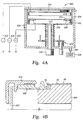
- Figure 4A is a cross sectional view of a physical vapor deposition (PVD) chamber adapted to deposit a full coverage seed layer on a substrate.
- PVD physical vapor deposition
- Figure 8 is a cut-away perspective view of a de-plating contact member according to the invention.
- the substrate support member 604 is raised to position the substrate thereon in a substrate processing position. At this position, a processing region is defined by the exposed surfaces of the target 606, the shield 608 and the substrate 40 on the substrate support member 604.
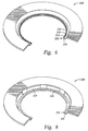
- the substrate support member 604 includes a deposition ring 642 disposed on a peripheral edge of the substrate support member 604.
- the actuator 620 elevates the substrate support member 604 to a substrate processing position, where the deposition ring 642 engages the bottom of the shield ring 624 and lifts the shield ring 624 off of the inner upturned wall of the shield 608.
- the inner portion of the shield ring 624 extends over an outer portion of the deposition ring 642.
- the shield ring 624 does not extend over the peripheral edge 42 of the substrate and allows full coverage deposition on the substrate 40.
- the substrate receives full deposition coverage over the whole substrate deposition surface and the substrate edge 42.
- the substrate also receives partial deposition on the peripheral portion of the backside surface 44 that extends outwardly from the substrate support.
- the full coverage deposition process provides a conformal seed layer 46 which extends over substantially all of the surface of the substrate on which the contacts in the cathode contact member of an electroplating system can be connected. By moving the contacts outwardly to the edge of the substrate, less than 3mm edge exclusion can be achieved as discussed below.
- the IMP-PVD processing parameters are adjusted to achieve a ratio of sidewall re-sputtering rate to deposition rate of up to about 2:3.
- the resulting deposition profile on the surfaces of the feature has a ratio of sidewall deposition thickness to base deposition thickness of between about 1:1 and 1:3.
- the chamber processing pressure is preferably maintained at between about 10 mTorr and about 100 mTorr, the RF source power to the IMP-PVD coil at between about 1000W and about 5000W, the target DC bias at between about 500W and about 3000W and substrate DC bias at between about 100W and about 500W.
- the seed layer preferably has a thickness between about 1500 ⁇ and about 2500 ⁇ over the field of the substrate, between about 150 ⁇ and about 300 ⁇ over the base surface of the feature and less than about 100 ⁇ , even more preferably, less than about 50 ⁇ , deposited on the sidewall portions of the feature.
- the substrate is transferred into an electrochemical deposition ceil to form a metal layer and fill interconnect features.
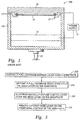
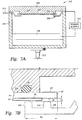
- Figure 5A is a cross sectional view of an electrochemical deposition cell adapted to achieve less than 3mm edge exclusion according to the invention.
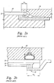
- Figure 5B is a cross sectional detail view of an edge portion of the substrate disposed on a substrate holder and a cathode contact member according to the invention.
- electrochemical deposition cells include the ElectraTM ECP System, available from Applied Material, Inc., Santa Clara, California, and the electrochemical deposition system described in commonly assigned and copending U.S. Patent Application No.
- the electrochemical deposition cell 200 generally comprises an electrolyte container 202, an anode 204, a substrate holder 206, and a cathode contact member 208.
- the electrolyte container 202 has a top opening adapted to receive a substrate disposed on the substrate holder and the cathode contact member.
- the electrolyte container 202 is connected to an electrolyte inlet 212 and an electrolyte outlet 214.
- the anode 204 is disposed in the electrolyte container 202 and electrically connected to a power supply 216.
- the substrate holder 206 preferably comprises a vacuum chuck 218 and an annular bladder 220 surrounding the vacuum chuck 218.
- the substrate is preferably transferred to a de-plating cell to remove the metal on the peripheral portion of the substrate, including the peripheral portion of the substrate deposition surface, the substrate bevel edge, and the peripheral portion of the substrate backside surface.
- the de-plating cell utilizes an electrolyte or an etching solution that selectively dissolves the seed layer material (e.g ., copper), but does not significantly dissolve or affect the barrier material or the substrate.
- the de-plating cell 300 generally comprises an electrolyte container 302, an anode 304 disposed in the electrolyte container, a de-plating substrate holder 306 and a de-plating contact member 308.
- the electrolyte container 302 has a top opening adapted to receive a substrate disposed on the de-plating substrate holder 306 and the de-plating contact member 308.
- the electrolyte container 302 is connected to an electrolyte inlet 312 and an electrolyte outlet 314.
- the anode 304 preferably comprising a non-consumable anode, is disposed in the electrolyte container 302 and electrically connected to a power supply 316.
- the substrate holder 306 preferably has a smaller diameter than the diameter of the substrate to expose a peripheral portion of the substrate backside surface that has the seed layer deposited thereon, and the annular seal 320 engages the substrate at a position radially inward of die peripheral portion of the substrate backside surface to expose the seed layer to the de-plating solution.
- the substrate surface can even be in physical contact with the surface of the de-plating contact 330 as long as there is sufficient contact resistance between the substrate surface and the surface of the de-plating contact 330.
- sufficient contact resistance exist between the substrate surface and the surface of the de-plating contact 330 to facilitate a de-plating process as described herein.
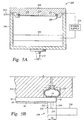
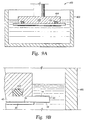
- FIG 9A is a cross sectional view of a wet etch cell according to another embodiment of the invention.
- Figure 9B is a cross sectional view of an edge portion of the substrate disposed in a wet etch cell of Figure 9A.
- the wet etch cell 400 generally comprises a container 402 and a substrate support 404.
- the container 402 holds the etch solution and includes a top opening adapted to receive a substrate disposed on an substrate support 404.
- the substrate holder 404 preferably comprises a vacuum chuck 408 and a seal 410, such as an o-ring, disposed around the vacuum chuck 408.
- the substrate holder 404 comprises a gripper, such as a vacuum gripper.
- the substrate support 404 is adapted to hold a substrate 40 on the backside surface of the substrate and expose the substrate deposition surface 50, the substrate edge 42, and the peripheral portion of the substrate backside surface 44 to the etch solution in the container 402.
- the substrate holder 404 submerges the substrate held thereon in the etching solution in the etching solution container 402.
- the etching solution comprises an etchant which dissolves the exposed metal into the solution.
- the etching solution may comprise citric acid, citric acid diluted with hydrogen peroxide (H 2 O 2 ) or other dilutants, or a combination of citric acid and sulfuric acid (H 2 SO 4 ) to dissolve an exposed copper layer.
- the etching solution is designed to provide selective etching of the seed layer material but leaves the barrier layer on the substrate.
- the seed layer is less than 10 percent of the total thickness of the electroplated metal layer, a 10% increase in the thickness of the electroplated metal layer or an increase corresponding to the thickness of the seed layer is sufficient to compensate for the de-plating effects.
- the electro-chemical deposition process is extended to deposit an additional 1000 ⁇ over the desired thickness so that during the wet etch process the seed layer is completely removed and the desired thickness for the electroplated layer remains on the substrate.
Landscapes
- Chemical & Material Sciences (AREA)
- Engineering & Computer Science (AREA)
- Chemical Kinetics & Catalysis (AREA)
- Electrochemistry (AREA)
- Materials Engineering (AREA)
- Metallurgy (AREA)
- Organic Chemistry (AREA)
- Life Sciences & Earth Sciences (AREA)
- Sustainable Development (AREA)
- Electrodes Of Semiconductors (AREA)
- Electroplating Methods And Accessories (AREA)
- ing And Chemical Polishing (AREA)
Applications Claiming Priority (2)
| Application Number | Priority Date | Filing Date | Title |
|---|---|---|---|
| US443832 | 1999-11-19 | ||
| US09/443,832 US6423636B1 (en) | 1999-11-19 | 1999-11-19 | Process sequence for improved seed layer productivity and achieving 3mm edge exclusion for a copper metalization process on semiconductor wafer |
Publications (2)
| Publication Number | Publication Date |
|---|---|
| EP1101839A2 true EP1101839A2 (fr) | 2001-05-23 |
| EP1101839A3 EP1101839A3 (fr) | 2004-01-21 |
Family
ID=23762366
Family Applications (1)
| Application Number | Title | Priority Date | Filing Date |
|---|---|---|---|
| EP00310208A Withdrawn EP1101839A3 (fr) | 1999-11-19 | 2000-11-17 | Procédé et appareil pour la formation de couches metalliques sur des substrats |
Country Status (5)
| Country | Link |
|---|---|
| US (1) | US6423636B1 (fr) |
| EP (1) | EP1101839A3 (fr) |
| JP (1) | JP5367930B2 (fr) |
| KR (1) | KR20010051801A (fr) |
| TW (1) | TW508661B (fr) |
Cited By (1)
| Publication number | Priority date | Publication date | Assignee | Title |
|---|---|---|---|---|
| US6689418B2 (en) | 2001-08-03 | 2004-02-10 | Applied Materials Inc. | Apparatus for wafer rinse and clean and edge etching |
Families Citing this family (28)
| Publication number | Priority date | Publication date | Assignee | Title |
|---|---|---|---|---|
| US6413436B1 (en) * | 1999-01-27 | 2002-07-02 | Semitool, Inc. | Selective treatment of the surface of a microelectronic workpiece |
| US6913680B1 (en) | 2000-05-02 | 2005-07-05 | Applied Materials, Inc. | Method of application of electrical biasing to enhance metal deposition |
| JP2004513221A (ja) * | 2000-05-23 | 2004-04-30 | アプライド マテリアルズ インコーポレイテッド | 銅シード層の異常を克服し表面形状サイズ及びアスペクト比を調整する方法と装置 |
| JP4055334B2 (ja) * | 2000-06-13 | 2008-03-05 | ソニー株式会社 | 半導体装置の製造方法 |
| US6534394B1 (en) * | 2000-09-13 | 2003-03-18 | International Business Machines Corporation | Process to create robust contacts and interconnects |
| EP1470268A2 (fr) * | 2000-10-03 | 2004-10-27 | Applied Materials, Inc. | Technique et dispositif connexe permettant d'incliner un substrat avant electrodeposition |
| US7189647B2 (en) | 2001-04-05 | 2007-03-13 | Novellus Systems, Inc. | Sequential station tool for wet processing of semiconductor wafers |
| US6572755B2 (en) * | 2001-04-11 | 2003-06-03 | Speedfam-Ipec Corporation | Method and apparatus for electrochemically depositing a material onto a workpiece surface |
| US6908540B2 (en) * | 2001-07-13 | 2005-06-21 | Applied Materials, Inc. | Method and apparatus for encapsulation of an edge of a substrate during an electro-chemical deposition process |
| KR100440261B1 (ko) * | 2001-12-22 | 2004-07-15 | 주식회사 하이닉스반도체 | 반도체 소자의 금속 배선 형성 방법 |
| US6733829B2 (en) * | 2002-03-19 | 2004-05-11 | Lsi Logic Corporation | Anti-binding deposition ring |
| US6911136B2 (en) * | 2002-04-29 | 2005-06-28 | Applied Materials, Inc. | Method for regulating the electrical power applied to a substrate during an immersion process |
| US7067045B2 (en) * | 2002-10-18 | 2006-06-27 | Applied Materials, Inc. | Method and apparatus for sealing electrical contacts during an electrochemical deposition process |
| US7025862B2 (en) * | 2002-10-22 | 2006-04-11 | Applied Materials | Plating uniformity control by contact ring shaping |
| KR20040072446A (ko) * | 2003-02-12 | 2004-08-18 | 삼성전자주식회사 | 반도체 기판의 가장자리 상의 금속막을 선택적으로제거하는 방법 |
| US20040229002A1 (en) * | 2003-05-15 | 2004-11-18 | 3D Systems, Inc. | Stereolithographic seal and support structure for semiconductor wafer |
| US7285195B2 (en) * | 2004-06-24 | 2007-10-23 | Applied Materials, Inc. | Electric field reducing thrust plate |
| US20090304914A1 (en) * | 2006-08-30 | 2009-12-10 | Lam Research Corporation | Self assembled monolayer for improving adhesion between copper and barrier layer |
| US20060175201A1 (en) * | 2005-02-07 | 2006-08-10 | Hooman Hafezi | Immersion process for electroplating applications |
| US7520969B2 (en) * | 2006-03-07 | 2009-04-21 | Applied Materials, Inc. | Notched deposition ring |
| US8062487B2 (en) * | 2007-06-25 | 2011-11-22 | United Microelectronics Corp. | Wafer supporting device of a sputtering apparatus |
| WO2011103214A1 (fr) * | 2010-02-16 | 2011-08-25 | Cypress Semiconductor Corporation | Blindage intégré pour dépôt de métal sur plaquette |
| US9905443B2 (en) * | 2011-03-11 | 2018-02-27 | Applied Materials, Inc. | Reflective deposition rings and substrate processing chambers incorporating same |
| WO2017092029A1 (fr) * | 2015-12-04 | 2017-06-08 | Acm Research (Shanghai) Inc. | Appareil pour le maintien d'un substrat |
| KR102323877B1 (ko) * | 2016-09-28 | 2021-11-10 | 한국전자통신연구원 | 전기 도금 장치 |
| US12191127B2 (en) * | 2018-10-31 | 2025-01-07 | Taiwan Semiconductor Manufacturing Company Ltd. | Apparatus for physical vapor deposition and method for forming a layer |
| JP7478109B2 (ja) * | 2021-02-24 | 2024-05-02 | 株式会社東芝 | 半導体装置の製造方法 |
| US12371790B2 (en) * | 2022-08-17 | 2025-07-29 | Sky Tech Inc. | Wafer carrier with adjustable alignment devices and deposition equipment using the same |
Family Cites Families (28)
| Publication number | Priority date | Publication date | Assignee | Title |
|---|---|---|---|---|
| US3835017A (en) * | 1972-12-22 | 1974-09-10 | Buckbee Mears Co | Reusable shields for selective electrodeposition |
| DE3272891D1 (en) | 1981-10-01 | 1986-10-02 | Emi Ltd | Electroplating arrangements |
| JPS58182823A (ja) | 1982-04-21 | 1983-10-25 | Nec Corp | 半導体ウエハ−のメツキ装置 |
| US4428815A (en) | 1983-04-28 | 1984-01-31 | Western Electric Co., Inc. | Vacuum-type article holder and methods of supportively retaining articles |
| US4605483A (en) * | 1984-11-06 | 1986-08-12 | Michaelson Henry W | Electrode for electro-plating non-continuously conductive surfaces |
| JPS63118093A (ja) | 1986-11-05 | 1988-05-23 | Tanaka Electron Ind Co Ltd | 電子部品の錫めつき方法 |
| US5224504A (en) * | 1988-05-25 | 1993-07-06 | Semitool, Inc. | Single wafer processor |
| US5235995A (en) * | 1989-03-27 | 1993-08-17 | Semitool, Inc. | Semiconductor processor apparatus with dynamic wafer vapor treatment and particulate volatilization |
| US5230743A (en) * | 1988-05-25 | 1993-07-27 | Semitool, Inc. | Method for single wafer processing in which a semiconductor wafer is contacted with a fluid |
| US5316974A (en) * | 1988-12-19 | 1994-05-31 | Texas Instruments Incorporated | Integrated circuit copper metallization process using a lift-off seed layer and a thick-plated conductor layer |
| US5222310A (en) * | 1990-05-18 | 1993-06-29 | Semitool, Inc. | Single wafer processor with a frame |
| US5259407A (en) * | 1990-06-15 | 1993-11-09 | Matrix Inc. | Surface treatment method and apparatus for a semiconductor wafer |
| US5256274A (en) * | 1990-08-01 | 1993-10-26 | Jaime Poris | Selective metal electrodeposition process |
| JPH04131395A (ja) | 1990-09-21 | 1992-05-06 | Toshiba Corp | 半導体ウエハのメッキ方法及び装置 |
| JP2697773B2 (ja) | 1991-03-11 | 1998-01-14 | 日本エレクトロプレイテイング・エンジニヤース 株式会社 | メッキ方法 |
| JP3200468B2 (ja) * | 1992-05-21 | 2001-08-20 | 日本エレクトロプレイテイング・エンジニヤース株式会社 | ウエーハ用めっき装置 |
| JPH0617291A (ja) | 1992-07-03 | 1994-01-25 | Nec Corp | 金属めっき装置 |
| US5486282A (en) * | 1994-11-30 | 1996-01-23 | Ibm Corporation | Electroetching process for seed layer removal in electrochemical fabrication of wafers |
| US5807469A (en) | 1995-09-27 | 1998-09-15 | Intel Corporation | Flexible continuous cathode contact circuit for electrolytic plating of C4, tab microbumps, and ultra large scale interconnects |
| WO1998027585A1 (fr) * | 1996-12-16 | 1998-06-25 | International Business Machines Corporation | Structures d'interconnexion plaquees sur microplaquettes de circuits integres |
| CN1168854C (zh) * | 1997-09-30 | 2004-09-29 | 塞米图尔公司 | 用于电镀半导体晶片的系统、装置和方法 |
| US6156167A (en) * | 1997-11-13 | 2000-12-05 | Novellus Systems, Inc. | Clamshell apparatus for electrochemically treating semiconductor wafers |
| US5897379A (en) * | 1997-12-19 | 1999-04-27 | Sharp Microelectronics Technology, Inc. | Low temperature system and method for CVD copper removal |
| US6140234A (en) * | 1998-01-20 | 2000-10-31 | International Business Machines Corporation | Method to selectively fill recesses with conductive metal |
| TW452828B (en) * | 1998-03-13 | 2001-09-01 | Semitool Inc | Micro-environment reactor for processing a microelectronic workpiece |
| US6416647B1 (en) * | 1998-04-21 | 2002-07-09 | Applied Materials, Inc. | Electro-chemical deposition cell for face-up processing of single semiconductor substrates |
| US6113771A (en) * | 1998-04-21 | 2000-09-05 | Applied Materials, Inc. | Electro deposition chemistry |
| US6056869A (en) * | 1998-06-04 | 2000-05-02 | International Business Machines Corporation | Wafer edge deplater for chemical mechanical polishing of substrates |
-
1999
- 1999-11-19 US US09/443,832 patent/US6423636B1/en not_active Expired - Fee Related
-
2000
- 2000-11-16 TW TW089124306A patent/TW508661B/zh not_active IP Right Cessation
- 2000-11-17 EP EP00310208A patent/EP1101839A3/fr not_active Withdrawn
- 2000-11-18 KR KR1020000068721A patent/KR20010051801A/ko not_active Withdrawn
- 2000-11-20 JP JP2000393798A patent/JP5367930B2/ja not_active Expired - Fee Related
Cited By (1)
| Publication number | Priority date | Publication date | Assignee | Title |
|---|---|---|---|---|
| US6689418B2 (en) | 2001-08-03 | 2004-02-10 | Applied Materials Inc. | Apparatus for wafer rinse and clean and edge etching |
Also Published As
| Publication number | Publication date |
|---|---|
| JP5367930B2 (ja) | 2013-12-11 |
| KR20010051801A (ko) | 2001-06-25 |
| JP2001240997A (ja) | 2001-09-04 |
| US6423636B1 (en) | 2002-07-23 |
| EP1101839A3 (fr) | 2004-01-21 |
| TW508661B (en) | 2002-11-01 |
Similar Documents
| Publication | Publication Date | Title |
|---|---|---|
| US6423636B1 (en) | Process sequence for improved seed layer productivity and achieving 3mm edge exclusion for a copper metalization process on semiconductor wafer | |
| US6399479B1 (en) | Processes to improve electroplating fill | |
| US6328871B1 (en) | Barrier layer for electroplating processes | |
| US6786996B2 (en) | Apparatus and method for edge bead removal | |
| US7138014B2 (en) | Electroless deposition apparatus | |
| US6503375B1 (en) | Electroplating apparatus using a perforated phosphorus doped consumable anode | |
| US7837841B2 (en) | Apparatuses for electrochemical deposition, conductive layer, and fabrication methods thereof | |
| US6280581B1 (en) | Method and apparatus for electroplating films on semiconductor wafers | |
| US8513124B1 (en) | Copper electroplating process for uniform across wafer deposition and void free filling on semi-noble metal coated wafers | |
| US20030140988A1 (en) | Electroless deposition method over sub-micron apertures | |
| US8703615B1 (en) | Copper electroplating process for uniform across wafer deposition and void free filling on ruthenium coated wafers | |
| WO2002019418A2 (fr) | Procede permettant d'obtenir un remplissage en cuivre presentant des caracteristiques d'interconnexions a rapport de forme eleve | |
| US20030143837A1 (en) | Method of depositing a catalytic layer | |
| US6808612B2 (en) | Method and apparatus to overcome anomalies in copper seed layers and to tune for feature size and aspect ratio | |
| US7416975B2 (en) | Method of forming contact layers on substrates | |
| US6708701B2 (en) | Capillary ring | |
| US20030073320A1 (en) | Method for preventing surface corrosion in an edge bead removal process | |
| US20070181434A1 (en) | Method and apparatus for fabricating metal layer | |
| US20040004004A1 (en) | Method for reducing cu surface defects following cu ECP | |
| US6652726B1 (en) | Method for reducing wafer edge defects in an electrodeposition process | |
| US20030209444A1 (en) | Method for reducing surface defects in an electrodeposition process | |
| US20100032315A1 (en) | Electrolytic processing apparatus and electrolytic processing method |
Legal Events
| Date | Code | Title | Description |
|---|---|---|---|
| PUAI | Public reference made under article 153(3) epc to a published international application that has entered the european phase |
Free format text: ORIGINAL CODE: 0009012 |
|
| AK | Designated contracting states |
Kind code of ref document: A2 Designated state(s): AT BE CH CY DE DK ES FI FR GB GR IE IT LI LU MC NL PT SE TR |
|
| AX | Request for extension of the european patent |
Free format text: AL;LT;LV;MK;RO;SI |
|
| PUAL | Search report despatched |
Free format text: ORIGINAL CODE: 0009013 |
|
| AK | Designated contracting states |
Kind code of ref document: A3 Designated state(s): AT BE CH CY DE DK ES FI FR GB GR IE IT LI LU MC NL PT SE TR |
|
| AX | Request for extension of the european patent |
Extension state: AL LT LV MK RO SI |
|
| RIC1 | Information provided on ipc code assigned before grant |
Ipc: 7C 23F 1/02 B Ipc: 7C 25F 3/14 B Ipc: 7C 25D 7/12 A |
|
| AKX | Designation fees paid | ||
| REG | Reference to a national code |
Ref country code: DE Ref legal event code: 8566 |
|
| STAA | Information on the status of an ep patent application or granted ep patent |
Free format text: STATUS: THE APPLICATION IS DEEMED TO BE WITHDRAWN |
|
| 18D | Application deemed to be withdrawn |
Effective date: 20040608 |