EP1102099A2 - Connecteur hybride - Google Patents
Connecteur hybride Download PDFInfo
- Publication number
- EP1102099A2 EP1102099A2 EP00107793A EP00107793A EP1102099A2 EP 1102099 A2 EP1102099 A2 EP 1102099A2 EP 00107793 A EP00107793 A EP 00107793A EP 00107793 A EP00107793 A EP 00107793A EP 1102099 A2 EP1102099 A2 EP 1102099A2
- Authority
- EP
- European Patent Office
- Prior art keywords
- connector
- optical
- element module
- receiving
- housing
- Prior art date
- Legal status (The legal status is an assumption and is not a legal conclusion. Google has not performed a legal analysis and makes no representation as to the accuracy of the status listed.)
- Withdrawn
Links
Images


Classifications
-
- G—PHYSICS
- G02—OPTICS
- G02B—OPTICAL ELEMENTS, SYSTEMS OR APPARATUS
- G02B6/00—Light guides; Structural details of arrangements comprising light guides and other optical elements, e.g. couplings
- G02B6/24—Coupling light guides
- G02B6/42—Coupling light guides with opto-electronic elements
- G02B6/4292—Coupling light guides with opto-electronic elements the light guide being disconnectable from the opto-electronic element, e.g. mutually self aligning arrangements
- G02B6/4293—Coupling light guides with opto-electronic elements the light guide being disconnectable from the opto-electronic element, e.g. mutually self aligning arrangements hybrid electrical and optical connections for transmitting electrical and optical signals
-
- G—PHYSICS
- G02—OPTICS
- G02B—OPTICAL ELEMENTS, SYSTEMS OR APPARATUS
- G02B6/00—Light guides; Structural details of arrangements comprising light guides and other optical elements, e.g. couplings
- G02B6/24—Coupling light guides
- G02B6/36—Mechanical coupling means
- G02B6/38—Mechanical coupling means having fibre to fibre mating means
- G02B6/3807—Dismountable connectors, i.e. comprising plugs
- G02B6/381—Dismountable connectors, i.e. comprising plugs of the ferrule type, e.g. fibre ends embedded in ferrules, connecting a pair of fibres
- G02B6/3817—Dismountable connectors, i.e. comprising plugs of the ferrule type, e.g. fibre ends embedded in ferrules, connecting a pair of fibres containing optical and electrical conductors
-
- G—PHYSICS
- G02—OPTICS
- G02B—OPTICAL ELEMENTS, SYSTEMS OR APPARATUS
- G02B6/00—Light guides; Structural details of arrangements comprising light guides and other optical elements, e.g. couplings
- G02B6/24—Coupling light guides
- G02B6/36—Mechanical coupling means
- G02B6/38—Mechanical coupling means having fibre to fibre mating means
- G02B6/3807—Dismountable connectors, i.e. comprising plugs
- G02B6/3869—Mounting ferrules to connector body, i.e. plugs
-
- G—PHYSICS
- G02—OPTICS
- G02B—OPTICAL ELEMENTS, SYSTEMS OR APPARATUS
- G02B6/00—Light guides; Structural details of arrangements comprising light guides and other optical elements, e.g. couplings
- G02B6/24—Coupling light guides
- G02B6/36—Mechanical coupling means
- G02B6/38—Mechanical coupling means having fibre to fibre mating means
- G02B6/3807—Dismountable connectors, i.e. comprising plugs
- G02B6/3873—Connectors using guide surfaces for aligning ferrule ends, e.g. tubes, sleeves, V-grooves, rods, pins, balls
- G02B6/3874—Connectors using guide surfaces for aligning ferrule ends, e.g. tubes, sleeves, V-grooves, rods, pins, balls using tubes, sleeves to align ferrules
- G02B6/3878—Connectors using guide surfaces for aligning ferrule ends, e.g. tubes, sleeves, V-grooves, rods, pins, balls using tubes, sleeves to align ferrules comprising a plurality of ferrules, branching and break-out means
- G02B6/3879—Linking of individual connector plugs to an overconnector, e.g. using clamps, clips, common housings comprising several individual connector plugs
-
- G—PHYSICS
- G02—OPTICS
- G02B—OPTICAL ELEMENTS, SYSTEMS OR APPARATUS
- G02B6/00—Light guides; Structural details of arrangements comprising light guides and other optical elements, e.g. couplings
- G02B6/24—Coupling light guides
- G02B6/36—Mechanical coupling means
- G02B6/38—Mechanical coupling means having fibre to fibre mating means
- G02B6/3807—Dismountable connectors, i.e. comprising plugs
- G02B6/389—Dismountable connectors, i.e. comprising plugs characterised by the method of fastening connecting plugs and sockets, e.g. screw- or nut-lock, snap-in, bayonet type
-
- G—PHYSICS
- G02—OPTICS
- G02B—OPTICAL ELEMENTS, SYSTEMS OR APPARATUS
- G02B6/00—Light guides; Structural details of arrangements comprising light guides and other optical elements, e.g. couplings
- G02B6/24—Coupling light guides
- G02B6/42—Coupling light guides with opto-electronic elements
- G02B6/4201—Packages, e.g. shape, construction, internal or external details
- G02B6/4219—Mechanical fixtures for holding or positioning the elements relative to each other in the couplings; Alignment methods for the elements, e.g. measuring or observing methods especially used therefor
- G02B6/4236—Fixing or mounting methods of the aligned elements
- G02B6/4245—Mounting of the opto-electronic elements
-
- G—PHYSICS
- G02—OPTICS
- G02B—OPTICAL ELEMENTS, SYSTEMS OR APPARATUS
- G02B6/00—Light guides; Structural details of arrangements comprising light guides and other optical elements, e.g. couplings
- G02B6/24—Coupling light guides
- G02B6/42—Coupling light guides with opto-electronic elements
- G02B6/4201—Packages, e.g. shape, construction, internal or external details
- G02B6/4255—Moulded or casted packages
-
- G—PHYSICS
- G02—OPTICS
- G02B—OPTICAL ELEMENTS, SYSTEMS OR APPARATUS
- G02B6/00—Light guides; Structural details of arrangements comprising light guides and other optical elements, e.g. couplings
- G02B6/24—Coupling light guides
- G02B6/42—Coupling light guides with opto-electronic elements
- G02B6/4201—Packages, e.g. shape, construction, internal or external details
- G02B6/4274—Electrical aspects
- G02B6/4277—Protection against electromagnetic interference [EMI], e.g. shielding means
-
- G—PHYSICS
- G02—OPTICS
- G02B—OPTICAL ELEMENTS, SYSTEMS OR APPARATUS
- G02B6/00—Light guides; Structural details of arrangements comprising light guides and other optical elements, e.g. couplings
- G02B6/24—Coupling light guides
- G02B6/42—Coupling light guides with opto-electronic elements
- G02B6/4201—Packages, e.g. shape, construction, internal or external details
- G02B6/4274—Electrical aspects
- G02B6/4284—Electrical aspects of optical modules with disconnectable electrical connectors
-
- G—PHYSICS
- G02—OPTICS
- G02B—OPTICAL ELEMENTS, SYSTEMS OR APPARATUS
- G02B6/00—Light guides; Structural details of arrangements comprising light guides and other optical elements, e.g. couplings
- G02B6/24—Coupling light guides
- G02B6/42—Coupling light guides with opto-electronic elements
- G02B6/4292—Coupling light guides with opto-electronic elements the light guide being disconnectable from the opto-electronic element, e.g. mutually self aligning arrangements
-
- G—PHYSICS
- G02—OPTICS
- G02B—OPTICAL ELEMENTS, SYSTEMS OR APPARATUS
- G02B6/00—Light guides; Structural details of arrangements comprising light guides and other optical elements, e.g. couplings
- G02B6/24—Coupling light guides
- G02B6/42—Coupling light guides with opto-electronic elements
- G02B6/4201—Packages, e.g. shape, construction, internal or external details
- G02B6/4246—Bidirectionally operating package structures
-
- G—PHYSICS
- G02—OPTICS
- G02B—OPTICAL ELEMENTS, SYSTEMS OR APPARATUS
- G02B6/00—Light guides; Structural details of arrangements comprising light guides and other optical elements, e.g. couplings
- G02B6/24—Coupling light guides
- G02B6/42—Coupling light guides with opto-electronic elements
- G02B6/4201—Packages, e.g. shape, construction, internal or external details
- G02B6/4251—Sealed packages
- G02B6/4253—Sealed packages by embedding housing components in an adhesive or a polymer material
-
- G—PHYSICS
- G02—OPTICS
- G02B—OPTICAL ELEMENTS, SYSTEMS OR APPARATUS
- G02B6/00—Light guides; Structural details of arrangements comprising light guides and other optical elements, e.g. couplings
- G02B6/24—Coupling light guides
- G02B6/42—Coupling light guides with opto-electronic elements
- G02B6/4201—Packages, e.g. shape, construction, internal or external details
- G02B6/4256—Details of housings
- G02B6/426—Details of housings mounting, engaging or coupling of the package to a board, a frame or a panel
- G02B6/4261—Packages with mounting structures to be pluggable or detachable, e.g. having latches or rails
-
- G—PHYSICS
- G02—OPTICS
- G02B—OPTICAL ELEMENTS, SYSTEMS OR APPARATUS
- G02B6/00—Light guides; Structural details of arrangements comprising light guides and other optical elements, e.g. couplings
- G02B6/24—Coupling light guides
- G02B6/42—Coupling light guides with opto-electronic elements
- G02B6/4201—Packages, e.g. shape, construction, internal or external details
- G02B6/4274—Electrical aspects
- G02B6/428—Electrical aspects containing printed circuit boards [PCB]
Definitions
- This invention relates to a hybrid connector including an electrical connector and an optical connector assembled to the electrical connector, which has the functions of the electrical connector and the optical connector.
- This invention has been accomplished to overcome the above drawback and an object of this invention is to provide a hybrid connector which is compact in size.
- a hybrid connector having an electrical connector and an optical connector assembled to the electrical connector
- the electrical connector comprising: an electrical housing having an open end through which to fit to a mating hybrid connector and a wall at an end thereof opposite the open end, the wall having a terminal mount section and an optical connector mount section juxtaposed to each other in a direction perpendicular to a connector fitting direction of the hybrid connector and the mating hybrid connector, and terminals bent L-shaped which are inserted at one end through the terminal mount section into the electrical housing to have bends thereof located outside the terminal mount section
- the optical connector comprising: an optical housing with an optical element module receiving section; a light emitting element module having a light emitting element; and a light receiving element module having a light receiving element, the light emitting element module and the light receiving element module being accommodated in the optical element module receiving section of the optical housing, wherein when the optical connector is assembled through the optical connector mount section to the electrical connector, the optical housing overlies at the optical element
- the optical housing at its optical element module receiving section overhangs or overlies the bends of the terminals with a spacing therebetween. Consequently, the size of the hybrid connector in a width direction thereof, i.e., in the direction perpendicular to the connector fitting direction becomes small by the length by which the optical housing overhangs the terminals.
- optical housing that overhangs serves to protect the terminals.
- hybrid connector used herein is intended to mean a connector with an electrical connector and an optical connector combined in one.
- the light emitting element is located off-center in the light emitting element module toward the light receiving element module
- the light receiving element is located off-center in the light receiving element module toward the light emitting element module.
- optical fiber cables leading to the mating optical connector can also be located close to each other, resulting in the mating optical connector and thus the optical connector made compact in size in the width direction.
- the optical housing has at the optical element module receiving section a terminal protector extending in the direction perpendicular to the connector fitting direction to overlie the bends of the terminals.
- the terminal protector serves to protect the terminals.
- the size of the hybrid connector in a width direction thereof, i.e., in the direction perpendicular to the connector fitting direction becomes small by the length by which the transmitting and receiving optical housings overhang the terminals. Further, the terminals are better protected.
- the emitting element is located off-center in the light emitting element module toward away from the terminals
- the light receiving element is located off-center in the light receiving element module toward away from the terminals.
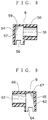
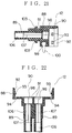
- a hybrid connector 1 of a male type which is implemented on a not-shown printed circuit board, includes a male electrical connector 2 and a male optical connector 3 assembled to the electrical connector 2.
- the optical connector 3 has a part thereof overhanging PCB terminals 4 of the electrical connector 2, so as to provide a compact construction.
- the electrical connector 2 includes a plurality of the PCB terminals 4 and an electrical housing 5.
- the optical connector 3 includes FOTs 6, 7 (FOT: fiber optical transceiver, also referred to as optical (light emitting or light receiving) element module) , FOT casings 8, 9, a shield casing 10, sleeves 11, 11, and an optical housing 12.
- FOTs 6, 7 FOT: fiber optical transceiver, also referred to as optical (light emitting or light receiving) element module
- FOT casings 8 9, a shield casing 10, sleeves 11, 11, and an optical housing 12.
- a hybrid connector 13 of a female type which mates with the hybrid connector 1 includes a female electrical connector 14, a female optical connector 15 assembled to the electrical connector 14, and a holder 16.
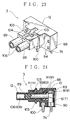
- the PCB terminals 4 are known electrically-conductive male terminals and, as shown in Fig. 2, bent in L-like form to be located at one end in the electrical housing 5 and fixed at the other end to the not-shown printed circuit board.
- the PCB terminals 4, in the present embodiment, are placed in two, upper and lower tiers (six for each tier) in the electrical housing 5 and thus provided in two types having different lengths.
- the electrical housing 5 is made of synthetic resin and, as shown in Figs. 4 to 7, has a bottomed box-like shape opening at the front.
- the electrical housing 5 has an upper wall 21 of rectangular shape when viewed from top, a bottom wall 22 parallel to the upper wall 21, a left and right side walls 23 and 24 contiguous to the upper and lower walls 21 and 22 at the lateral ends, and a rear wall 26 located at a side opposite the insertion open end 25 for the mating hybrid connector 13 (Fig. 3) , which rear wall is contiguous to the upper, lower, left and right side walls 21, 22, 23 and 24.
- the lower wall 22 is formed at its inner side with guide grooves 32, 32.
- the engagement dent 29 extends straight at a center of the upper wall 21, from the open end 25 to an inner surface of the rear wall 26, and has a rectangular section under the upper wall 21. There are formed slits 33, 33 in the upper wall 21, which are in communication with the engagement dent 29 and extend from near the open end 25 to the rear wall 26.
- the guide grooves 30, 30 extend straight at the lateral ends of the upper wall 21, from the open end 25 to the inner surface of the rear wall 26, and are laterally defined by the respective left and right side walls 23 and 24.
- the guide grooves 30, 30 have a rectangular section under the upper wall 21.
- the guide grooves 30, 30 have a depth equal to the engagement dent 29, but a width smaller than the latter.
- the guide groove 31 is interposed between the engagement dent 29 and the guide groove 30 on the side of the right side wall 24, and extends straight from the open end 25 to the inner surface of the rear wall 26.
- the guide groove 31 also has a rectangular section under the upper wall 21 and has a depth roughly one half that of the guide grooves 30, 30 and a width equal to the latter.
- the guide grooves 32, 32 are formed at the lateral ends of the lower wall 22, in opposition to the respective guide grooves 30, 30 and are laterally defined by the respective left and right side walls 23 and 24.
- the guide grooves 32, 32 have a rectangular section on the lower wall 22.
- the guide grooves 32, 32 like the guide grooves 30, 30 and 31 formed on the upper wall 21, extend straight from the open end 25 to the inner surface of the rear wall 26.
- the guide grooves 32, 32 have a depth smaller than the guide groove 31 and a width equal to the guide grooves 30, 30.
- the left and right side walls 23 and 24 are provided with a mounting portion 36 with which to mount on the not-shown printed circuit board.
- the mounting portion 36 is roughly semicircular when viewed from top and has a height approximately one fourth the height of the left and right walls 23, 24.
- the mounting portion 36 has a lower surface flush with the lower wall 22 and a clip 37 at the lower surface for insertion through elastic deformation through and engagement with a corresponding hole formed in the not-shown printed circuit board.
- the rear wall 26 is flat and perpendicular to the upper, lower, left and right side walls 21, 22, 23, 24 and has a PCB terminal mount section 40 and an optical connector mount section 41 juxtaposed to each other.
- the PCB terminal mount section 40 is located toward the right side wall 24 and receives the PCB terminals 4 at the one end side in two tiers into the electrical housing 5.
- the PCB terminals 4 are pressed into at the terminal mount section 40 or insert-molded to form the electrical connector 2.
- the bends of the PCB terminals 4 in the upper tier are located remoter from the rear wall 26 than those of the PCB terminals 4 in the lower tier.
- the optical connector mount section 41 is located toward the left side wall 23 and includes a holder portion 42 (Fig. 7) projecting from the rear wall 26 and an insertion opening 43 for the optical connector 3 (Fig. 2).
- the insertion opening 43 extends in the connector fitting direction through the holder portion 42 and the rear wall 26 to communicate to the inside of the electrical housing 5.
- the insertion opening 43 has a rectangular cross section and is formed with a taper surface 45 at the corner between the lower and left side walls 22 and 23, which taper surface extends longitudinally of the insertion opening 43.
- the taper surface 45 serves to prevent an erroneous fitting of the optical connector 3 (Fig. 2).
- the taper surface 45 may be located at other than the above-mentioned corner and may be replaced by a projection or groove as far as serving the above effect.
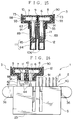
- the FOT 6, as shown in Fig. 2, includes a molded portion 49 and a plurality of leads 48 extending from the molded portion.
- One of the leads 48 is mounted with a light emitting element (not shown) . Wire bonding is also effected.
- the leads 48 are fixed (soldered) at the lower end to the not-shown printed circuit board.
- the not-shown light emitting element is disposed not at the center of the FOT 6 (or of the molded portion 49) , but rather at a side toward the FOT 7.
- the light emitting element may be located at the center, but, as will be described later, off-center arrangement toward the FOT 7 serves to make the hybrid connector 1 compact in size.
- a light emitting diode (LED), for example, can be mentioned as the light emitting element of the FOT (light emitting element module) 6.
- the molded portion 49 is molded to have a rectangular cross section from transparent resin material capable of transmitting light (for example, epoxy resin preferably having the same refractive index as that of a later-described plastic optical fiber 121).
- the leads 48 are embedded at the upper end in the molded portion 49.
- the molded portion 49 protects the light emitting element and the like from outside.
- the FOT 7 as shown in Fig. 2, includes a molded portion 51 and a plurality of leads 50 extending from the molded portion.
- One of the leads 50 is mounted with a light receiving element (not shown) . Wire bonding is also effected.
- the leads 50 are fixed (soldered) at the lower end to the not-shown printed circuit board.
- the not-shown light receiving element is disposed not at the center of the FOT 7 (or of the molded portion 51) , but rather at a side toward the FOT 6.
- the light receiving element may be located at the center, but, as will be described later, off-center arrangement toward the FOT 6 serves to make the hybrid connector 1 compact in size.
- a photodiode (PD), for example, can be mentioned as the light receiving element of the FOT (light receiving element module) 7.
- the molded portion 51 like the molded portion 49, is molded to have a rectangular cross section from transparent resin material capable of transmitting light (for example, epoxy resin preferably having the same refractive index as that of the later-described plastic optical fiber 121).
- the leads 50 are embedded at the upper end in the molded portion 51.
- the molded portion 51 protects the light receiving element and the like from outside.
- the optical fiber cables 115, 115 (Fig. 3) of the mating optical connector 15 located close to each other, resulting in the mating optical connector 15 (Fig. 3) itself made compact in size, which in turn makes the electrical housing 5 (Fig. 2) compact in size.
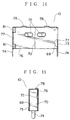
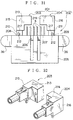
- the FOT casing 8 is made of conductive synthetic resin material containing carbon fibers or the like (may also be made of insulating synthetic resin material, though) and, as shown in Figs. 2 and 8, includes a case body 54 for covering the molded portion 49 of the FOT 6 and a cylindrical portion 55 projecting from the case body 54.
- the case body 54 as shown in Fig. 8, has a bottomed box-like shape.
- the molded portion 49 of the FOT 6 is pressingly inserted into the case body 54.
- the case body 54 has a rectangular cutout 56 at the insertion open end for the FOT 6, i.e., in the side wall 57 at the side remote from the cylindrical portion 55.
- the cylindrical portion 55 is located at a position corresponding to the light emitting element (not shown) of the FOT 6, pressingly receives the related sleeve 11 (Fig. 2) , and is formed with a flat surface 58 cut thereon which is flush with the upper wall 59 of the case body 54.
- the flat surface 58 is formed for placing the FOT 6 in position.
- the FOT casing 9, like the FOT casing 8, is made of conductive synthetic resin material containing carbon fibers or the like (may also be made of insulating synthetic resin material, though) and, as shown in Figs. 2 and 9, includes a case body 62 for covering the molded portion 51 of the FOT 7 and a cylindrical portion 63 projecting from the case body 62.
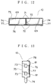
- the convex portions 72, 72 have an oval shape and are formed by striking to project on the rear wall 76 of the receiving sections 69, 69, at positions corresponding to the cutouts 71, 71.
- Each convex portion 72 is provided with a circumferential taper.
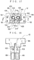
- the terminal protector 200 as shown in Figs. 29 and 30, includes a rectangular plate or piece extending from the optical housing 102 at the FOT receiving section 88, in a direction in which the PCB terminal mount section 40 and the optical connector mount section 41 are juxtaposed.
- the terminal protector 200 overhangs the bends of the PCB terminals 4, with a spacing therebetween.
- the terminal protector 200 makes an improvement over the hybrid connector 1 (Figs. 1 and 2) , in the effect of protecting the terminals.
Landscapes
- Physics & Mathematics (AREA)
- General Physics & Mathematics (AREA)
- Optics & Photonics (AREA)
- Electromagnetism (AREA)
- Optical Couplings Of Light Guides (AREA)
Applications Claiming Priority (4)
| Application Number | Priority Date | Filing Date | Title |
|---|---|---|---|
| JP32905999A JP2001147346A (ja) | 1999-11-19 | 1999-11-19 | 雌コネクタ |
| JP32905999 | 1999-11-19 | ||
| JP34849999A JP3646979B2 (ja) | 1999-12-08 | 1999-12-08 | ハイブリッドコネクタ |
| JP34849999 | 1999-12-08 |
Publications (2)
| Publication Number | Publication Date |
|---|---|
| EP1102099A2 true EP1102099A2 (fr) | 2001-05-23 |
| EP1102099A3 EP1102099A3 (fr) | 2002-10-02 |
Family
ID=26573072
Family Applications (1)
| Application Number | Title | Priority Date | Filing Date |
|---|---|---|---|
| EP00107793A Withdrawn EP1102099A3 (fr) | 1999-11-19 | 2000-04-11 | Connecteur hybride |
Country Status (1)
| Country | Link |
|---|---|
| EP (1) | EP1102099A3 (fr) |
Cited By (6)
| Publication number | Priority date | Publication date | Assignee | Title |
|---|---|---|---|---|
| EP1170612A3 (fr) * | 2000-07-03 | 2004-03-24 | Yazaki Corporation | Connecteur hybride optique et électrique |
| EP1170609A3 (fr) * | 2000-07-03 | 2004-03-24 | Yazaki Corporation | Connecteur hybride et procédé pour son assemblage |
| EP1158329A3 (fr) * | 2000-05-23 | 2004-06-23 | Yazaki Corporation | Connecteur optique |
| DE102007062658A1 (de) | 2007-12-24 | 2009-06-25 | Bktel Communications Gmbh | Hybrid-Steckverbindung |
| DE102008014795B4 (de) * | 2007-07-25 | 2010-04-29 | Yazaki Corp. | Optikmodul |
| WO2022142848A1 (fr) * | 2020-12-29 | 2022-07-07 | 华为技术有限公司 | Ensemble cage optique, connecteur de module optique et procédé de fabrication pour ensemble cage optique |
Family Cites Families (5)
| Publication number | Priority date | Publication date | Assignee | Title |
|---|---|---|---|---|
| US4678264A (en) * | 1983-03-30 | 1987-07-07 | Amp Incorporated | Electrical and fiber optic connector assembly |
| US4993803A (en) * | 1989-05-18 | 1991-02-19 | General Motors Corporation | Electro-optical header connector |
| US5121454A (en) * | 1989-11-24 | 1992-06-09 | Nippon Telegraph And Telephone Corporation | Optical connector |
| US5325454A (en) * | 1992-11-13 | 1994-06-28 | International Business Machines, Corporation | Fiber optic connector housing |
| US5419717A (en) * | 1994-08-15 | 1995-05-30 | The Whitaker Corporation | Hybrid connector between optics and edge card |
-
2000
- 2000-04-11 EP EP00107793A patent/EP1102099A3/fr not_active Withdrawn
Cited By (7)
| Publication number | Priority date | Publication date | Assignee | Title |
|---|---|---|---|---|
| EP1158329A3 (fr) * | 2000-05-23 | 2004-06-23 | Yazaki Corporation | Connecteur optique |
| EP1170612A3 (fr) * | 2000-07-03 | 2004-03-24 | Yazaki Corporation | Connecteur hybride optique et électrique |
| EP1170609A3 (fr) * | 2000-07-03 | 2004-03-24 | Yazaki Corporation | Connecteur hybride et procédé pour son assemblage |
| DE102008014795B4 (de) * | 2007-07-25 | 2010-04-29 | Yazaki Corp. | Optikmodul |
| DE102007062658A1 (de) | 2007-12-24 | 2009-06-25 | Bktel Communications Gmbh | Hybrid-Steckverbindung |
| EP2075604A1 (fr) | 2007-12-24 | 2009-07-01 | Bktel Communications Gmbh | Connexion à fiches hybride electrique-optique du type RJ-45 |
| WO2022142848A1 (fr) * | 2020-12-29 | 2022-07-07 | 华为技术有限公司 | Ensemble cage optique, connecteur de module optique et procédé de fabrication pour ensemble cage optique |
Also Published As
| Publication number | Publication date |
|---|---|
| EP1102099A3 (fr) | 2002-10-02 |
Similar Documents
| Publication | Publication Date | Title |
|---|---|---|
| US6341899B1 (en) | Hybrid connector | |
| US6499889B1 (en) | Method of assembling optical connector, optical connector and hybrid connector | |
| US6357931B1 (en) | Hybrid connector | |
| US6558045B2 (en) | Hybrid connector and assembling method thereof | |
| US6547446B2 (en) | Hybrid connector | |
| US6500026B2 (en) | Hybrid connector and process for assembling the same | |
| KR100486474B1 (ko) | 커넥터 | |
| CA1246915A (fr) | Connecteur de fibre optique | |
| EP1217407B1 (fr) | Connecteur composé optique/électrique | |
| US8616787B2 (en) | Optical connector and manufacturing method thereof | |
| JP2015500517A (ja) | 光モジュール | |
| JP3778479B2 (ja) | 発光素子モジュール及び受光素子モジュールの位置決め方法、光コネクタ、及びハイブリッドコネクタ | |
| US7090410B2 (en) | Optical receptacle with low transmission loss and photoelectric conversion module for the same | |
| EP1102099A2 (fr) | Connecteur hybride | |
| JP3654574B2 (ja) | ハイブリッドコネクタの支持構造 | |
| GB2356465A (en) | Optic fibre connector with light emitter and receiver in casing | |
| JP2002023026A (ja) | 光コネクタ | |
| JP2001166182A (ja) | 光コネクタの組み付け方法、光コネクタ、及びハイブリッドコネクタ | |
| JP2002023027A (ja) | 光コネクタ | |
| JP3950583B2 (ja) | 光伝送モジュール | |
| JP2005091416A (ja) | 光ファイバ保持構造、光ファイバ保持部品、及び光モジュール | |
| CN113009645A (zh) | 一种光模块 |
Legal Events
| Date | Code | Title | Description |
|---|---|---|---|
| PUAI | Public reference made under article 153(3) epc to a published international application that has entered the european phase |
Free format text: ORIGINAL CODE: 0009012 |
|
| AK | Designated contracting states |
Kind code of ref document: A2 Designated state(s): AT BE CH CY DE DK ES FI FR GB GR IE IT LI LU MC NL PT SE |
|
| AX | Request for extension of the european patent |
Free format text: AL;LT;LV;MK;RO;SI |
|
| PUAL | Search report despatched |
Free format text: ORIGINAL CODE: 0009013 |
|
| AK | Designated contracting states |
Kind code of ref document: A3 Designated state(s): AT BE CH CY DE DK ES FI FR GB GR IE IT LI LU MC NL PT SE |
|
| AX | Request for extension of the european patent |
Free format text: AL;LT;LV;MK;RO;SI |
|
| 17P | Request for examination filed |
Effective date: 20030207 |
|
| AKX | Designation fees paid |
Designated state(s): DE FR GB IT SE |
|
| 17Q | First examination report despatched |
Effective date: 20030515 |
|
| STAA | Information on the status of an ep patent application or granted ep patent |
Free format text: STATUS: THE APPLICATION IS DEEMED TO BE WITHDRAWN |
|
| 18D | Application deemed to be withdrawn |
Effective date: 20060627 |