EP1102158B1 - Gerät und Verfahren für die Kontrolle des Betriebszustandes eines elektronischen Systems in einem Graubereich - Google Patents
Gerät und Verfahren für die Kontrolle des Betriebszustandes eines elektronischen Systems in einem Graubereich Download PDFInfo
- Publication number
- EP1102158B1 EP1102158B1 EP19990123091 EP99123091A EP1102158B1 EP 1102158 B1 EP1102158 B1 EP 1102158B1 EP 19990123091 EP19990123091 EP 19990123091 EP 99123091 A EP99123091 A EP 99123091A EP 1102158 B1 EP1102158 B1 EP 1102158B1
- Authority
- EP
- European Patent Office
- Prior art keywords
- reset
- microprocessor
- supply voltage
- signal
- power
- Prior art date
- Legal status (The legal status is an assumption and is not a legal conclusion. Google has not performed a legal analysis and makes no representation as to the accuracy of the status listed.)
- Expired - Lifetime
Links
Images


Classifications
-
- G—PHYSICS
- G06—COMPUTING OR CALCULATING; COUNTING
- G06F—ELECTRIC DIGITAL DATA PROCESSING
- G06F1/00—Details not covered by groups G06F3/00 - G06F13/00 and G06F21/00
- G06F1/24—Resetting means
-
- G—PHYSICS
- G06—COMPUTING OR CALCULATING; COUNTING
- G06F—ELECTRIC DIGITAL DATA PROCESSING
- G06F1/00—Details not covered by groups G06F3/00 - G06F13/00 and G06F21/00
- G06F1/26—Power supply means, e.g. regulation thereof
- G06F1/30—Means for acting in the event of power-supply failure or interruption, e.g. power-supply fluctuations
Definitions
- the present invention relates to a device for controlling the operating state of an electronic system, in particular of a low-power electronic system, powered by a source of electrical energy supply, this electronic system including in particular a microprocessor capable of operate at a guaranteed minimum level of operation.
- a device is in particular intended to provide a signal, said "reset” signal, keeping the microprocessor in a determined state, called “reset” state, as long as the power supply voltage delivered by the power source is lower. at a determined voltage level.
- the present invention also relates to an electronic system equipped with the aforementioned device and a method for controlling the operating state of such an electronic system.
- gray zone will be used in the remainder of this description to denote an area in which at least one microprocessor of an electronic system is powered by a supply voltage whose level is below the minimum guaranteed operating level of this system. microprocessor, and wherein the microprocessor is no longer in a state of zeroing determined, said state of "reset". It will be understood from the following that when such a microprocessor is in this "gray area", it can potentially perform operations or execute erroneous instructions.
- a power-on-reset cell is provided, or more commonly a “power-on-reset” cell whose threshold is greater than the operating level. guaranteed minimum that the microprocessor can operate on. It is thus ensured that, when the power supply source is switched on, the microprocessor is maintained in a determined “reset” state until the supply voltage has reached a level greater than its level. guaranteed minimum operation.
- a low power electronic system powered by an electrical power source of the order of 5 volts and comprising a microprocessor whose minimum operating threshold determined is of the order of 1.9 volts.
- An example of such a low-power electronic system is in particular marketed by the Applicant, the company EM Microelectronic-Marin SA, under the reference EM6640 "4 bit Microcontroller”.
- the typical approach mentioned above would be to use a power-up zeroing cell with a threshold greater than the minimum guaranteed operating level of the microprocessor, ie a threshold of at least 2 Volts to account for tolerances. manufacturing and variations due to temperature.
- This approach is also used in the patent application EP 0 604 270 which, in addition, uses a voltage drop detector to compare a voltage drop of the supply voltage V with a predetermined voltage drop value V1 to put said microprocessor in a "reset" state if a fall of the supply voltage V is detected greater than the predetermined value V1.
- a low voltage zero-setting cell or at least may become smaller than the minimum guaranteed operating level of the microprocessor. It follows the appearance of the so-called "gray zone", mentioned above, defined by the voltage range between the threshold of the zero-voltage cell and the guaranteed minimum operating level of the microprocessor. In this zone, the microprocessor is likely to execute erroneous instructions which may have adverse consequences on the operation of the system. In particular, erroneous data that can be used as a code, such as an encryption code, could be written into a non-volatile memory (EEPROM) of the system.
- EEPROM non-volatile memory
- An object of the present invention is thus to allow the use of a zero-powered reset cell having a low threshold of zero while ensuring that the microprocessor can not execute instructions during its transition to "gray area” and avoiding a transition to "gray area” when a decrease in supply voltage.
- the present invention thus relates to a device for controlling the operation of a low power electronic system whose characteristics are set forth in claim 1.
- the present invention also relates to a low power electronic system whose characteristics are set forth in claim 4.
- the present invention further relates to a method of controlling the operation of a low power electronic system whose characteristics are set forth in claim 5.
- An advantage of the present invention is that the lifetime of the power source is increased by the use of a zero-voltage cell having a low zeroing threshold.
- Another advantage of the present invention lies in the fact that this prevents microprocessor execution of erroneous instructions both at the start of the microprocessor and when a voltage drop occurs during its operation.
- Yet another advantage of the present invention is that simple logic means are employed to extend the "reset" state of the microprocessor. These logic means can moreover be perfectly integrated directly on the system without this implying an additional manufacturing cost.
- the figure 1 shows a block diagram of a low power electronic system generally indicated by reference numeral 1 constituting an embodiment of the present invention.
- This electronic system 1 is powered by an electric power source 5.
- this source of power supply 5 is typically a battery delivering a low supply voltage, as an illustration of the order of 5.5 volts.
- This source of electric power supply 5 is connected to a power supply unit 40 which is arranged to supply, at a first of its terminals 40.1, a supply voltage V DD referenced with respect to a ground voltage V SS , defined at one second from its terminals 40.2.
- Each component of the electronic system 1 thus comprises a first power supply terminal, not shown, for receiving the supply voltage V DD , and a second power supply terminal, not shown, for receiving the ground voltage V SS .
- the electronic system 1 illustrated in figure 1 comprises at least one central processing unit or microprocessor 10 as well as a set of peripherals, not shown in this figure, notably comprising storage means (ROM, RAM, EEPROM), an input port and an output port.
- the microprocessor 10 is adapted to operate correctly from a guaranteed minimum operating level V DD, min .
- V DD minimum operating level
- the microprocessor 10 can thus function correctly from a minimum guaranteed level of operation V DD.min of the order of 1.9 volts.
- the electronic system 1 further comprises a system clock 20, comprising for example an RC oscillator, not shown, arranged to deliver at least one clock signal to the system components.
- the system clock 20 thus comprises for example outputs 20.1 and 20.2 each providing a clock signal CLK1 or CLK2 respectively.
- the output 20.1 of the system clock is thus connected to an input or clock input 10.1 of the microprocessor 10.
- the basic frequency of the clock signal is for example of the order of 600 kHz, but the system clock 20 can nevertheless provide clock signals at sub-multiples of the base frequency.
- the system clock 20 is thus typically provided with a division chain, not shown, for deriving a desired frequency from the abovementioned basic frequency.
- the system clock 20 is for example arranged to provide a clock signal having a frequency of the order of 1 kHz to a functional block 33 of the electronic system 1 of the figure 1 . It goes without saying that numerical values mentioned in the present description are only illustrative only.
- the electronic system 1 also comprises zeroing means generally indicated by the dashed lines and denoted by the reference numeral 30. These zeroing means 30 ensure in particular a maintenance of the microprocessor 10 in a determined state of "reset".
- the microprocessor 10 comprises a "reset” input, referenced 10.R, on which a CPU RST "reset” logic signal is applied.
- the microprocessor 10 is for example maintained in the “reset” state as long as the CPU signal RST applied to its "reset” input 10.R is at a "high” logic level.
- the microprocessor 10 is then released from its "reset” state.
- the zeroing means 30 can be broken down into two subsets.
- a first of these subsets consists of a power-on-reset cell 32, more commonly referred to as a "power-on-reset" cell.
- a second of these subsets consists of a first and a second functional block respectively identified by the reference numerals 33 and 34, and which will be discussed in more detail later in this description.
- the power-up zeroing cell 32 is typically arranged to deliver a "reset” signal or, more exactly, a power-up zeroing signal POR as soon as the system 1 is switched on.
- This cell 32 produces in particular this signal " reset "POR during a change of the battery 5, that is to say in a situation where the supply voltage V DD of the system increases from a substantially zero level (from V SS ).
- this power-on zero-latch cell 32 provides a power-on zero-turn signal POR which takes a first logic level as long as the power supply voltage V DD does not exceed a threshold, referred to as the zero-point threshold.
- voltage V POR and which goes to a second logic level when this supply voltage V DD exceeds this threshold of zero voltage V POR .
- the "reset” signal POR is delivered to an output 32.1 of the power-on reset cell 32 on “reset” inputs of various components, in particular the “reset” input 20.R of the system clock. 20 and the “reset” inputs 33.R and 34.R of the first and second functional blocks 33 and 34. In the remainder of the description, the inputs will be identified. of “reset” of the various components of the system by the index “R” attached to the numerical reference of the corresponding component.
- the live zeroing cell 32 is continuously powered and is arranged to provide the "reset" signal POR which adopts a first logic level, for example the “low” logic level, as long as the supply voltage V DD of the battery 5 does not exceed the determined voltage-off threshold V POR , and which adopts a second logic level, for example the "high” logic level, beyond the power-off threshold V POR .
- the various components are set to zero or maintained in the "reset” state when a "high” logic level signal is applied to their "reset” input.
- the "reset” inputs 20.R, 33.R and 34.R of the system clock 20 and the two function blocks 33 and 34 are reversed, as shown in FIG. figure 1 , so that the corresponding components are set to zero as long as the power-off signal POR remains at the "low” logic level.
- the voltage-zeroing threshold V POR of the power-on zeroing cell 32 is, or can be defined low, and in particular smaller than the minimum guaranteed operating level V DD, min at which can be used correctly microprocessor 10.
- the threshold for zeroing voltage V POR is of the order of 1.5 volts, which is lower than the guaranteed minimum level V DD, min of 1.9 volts cited above also as an illustration.
- the microprocessor 10 is thus may perform erroneous operations, including giving erroneous write instructions in a system memory, if it is not maintained in a state of "reset". It will now be described how this situation is avoided according to the present invention.
- the first functional block 33 of the figure 1 is arranged, on the one hand, to delay the release of the "reset” state of the system, and in particular the release of the "reset” state of the microprocessor 10, for a determined minimum period ⁇ t STAB .
- This period ⁇ t STAB is chosen in particular so as to allow a stabilization of the oscillator RC of the system clock 20 when it is activated.
- this period ⁇ t STAB is for example of the order of 1 ms. It is therefore also possible to qualify the first functional block 33 as a delay block.
- This delay block 33 comprises in particular a clock input 33.C connected to the output 20.2 of the system clock 20 which delivers the clock signal CLK2 at a frequency of, for example, 1 kHz.
- the "reset" signal CPU RST of the microprocessor 10 is produced at an output 33.2 of the delay block 33.
- this first functional block 33 is, on the other hand, arranged to delay the release of the "reset" state of the microprocessor 10 as long as the supply voltage V DD delivered by the battery is not greater than the minimum guaranteed operating level V DD, min of the microprocessor.
- the electronic system 1 further comprises a second functional block or detection block, identified by the reference numeral 34. This detection block is arranged to monitor the supply voltage V DD delivered by the battery 5, and for provide at least a first control logic signal representative of the level of this supply voltage V DD .
- the detection block 34 is arranged to supply, at a first output 34.1, a first ENBL CPU control logic signal which takes a first logic level, for example a "low” logic level, if the supply voltage V DD is less than a first determined reference threshold V REF1 , and which takes a second logic level, for example a "high” logic level, if the supply voltage V DD is greater than the reference threshold V REF1 , this first threshold reference V REF1 is chosen greater than or equal to the minimum guaranteed operating level V DD, min of the microprocessor 10.
- This first ENBL CPU control signal is delivered to an input 33.1 of the delay block 33.
- the first functional block or delay block 33 thus releases the "reset" state of the microprocessor 10, that is to say the CPU RST “reset” signal of the logic level “high”. “at the logic” low “level, at the earliest after the determined time interval ⁇ t STAB allowing the stabilization of the RC oscillator of the system clock 20. If, at the end of this determined time interval ⁇ t STAB , the block detection circuit 34 indicates that the supply voltage V DD has not reached the set reference threshold V REF1 greater than the minimum guaranteed operating level V DD, min of the microprocessor 10, the release of the "reset” state n Then, when the detection block provides a logic level CPU signal ENBL "high".
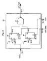
- the figure 2 thus shows an example of a delay block that can be used to fulfill the function of the delay block 33 of the figure 1 .
- This delay block also identified by the reference numeral 33, comprises first and second flip-flops 35 and 36 each comprising a clock input 35.C, respectively 36.C, a reset input 35.R, respectively 36.R, a data input 35.1, respectively 36.1, and an output 35.2, respectively 36.2.
- the delay block 33 further comprises a NAND gate 37 provided with two inputs respectively connected to the outputs 35.2 and 36.2 of the first and second flip-flops 35 and 36, the output of which produces the "reset" signal CPU RST via the output 33.2 of the delay block 33.
- This NAND gate 37 performs the logic function "NAND", that is to say produces at its output a logic signal "low” only if its two inputs are at the logic level "high”.
- the "reset" inputs 35.R and 36.R of the flip-flops 35 and 36 are connected together to the inverted "reset" input 33.R of the delay block so that the flip-flops 35 and 36 are simultaneously zeroed. when the "reset" signal POR produced by the power-on reset cell 32 occupies the "low” logic level.
- a "high” logic level signal is continuously applied to the data inputs 35.1 and 36.1 of the flip-flops 35 and 36.
- the clock signal CLK2 delivered by the system clock 20 to the clock input 33.C of the delay block 33 is applied to the clock input 35.C of the first flip-flop 35.
- This clock input 35.C is here reversed. This indicates, by convention, that the output 35.2 of the flip-flop 35 goes to the logic "high” level which is applied to the data input 35.1 on a falling edge of the clock signal CLK2.
- the clock signal CLK2 typically has a frequency of the order of 1 kHz so that the output 35.2 of the first flip-flop 35 switches to the logic level "high" at the end of a period ( ⁇ t STAB ) of the order of 1 ms on a falling edge of the clock signal CLK2.
- the ENBL CPU control signal from the detection block 34 is applied via the input 33.1 of the delay block to the clock input 36.C of the second flip-flop 36.
- This clock input 36.C is not reversed so that the output 36.2 of the second flip-flop 35 passes, by convention, at the "high" logic level which is applied to the data input 36.1 on a rising edge of the clock signal applied to its clock input , ie on a rising edge of the ENBL CPU control signal.
- the output 35.2 goes on and remains at the "high” logic level as soon as a falling edge of the clock signal CLK2, respectively a rising edge of the ENBL CPU control signal, appears at the clock input 35.C, respectively the clock input 36.C.
- the "reset” signal CPU RST appearing at the output of the NAND gate thus goes to the “low” logic level, releasing the "reset” state of the microprocessor when the two outputs 35.2 and 36.2 are at the "high” logic level.
- the reference threshold V REF1 of the detection block 34 is chosen to be lower but close to the maximum supply voltage that can be delivered by the electrical power supply source 5, so that the microprocessor 10 is maintained at the same time. state of "reset” if a defective or expired power source, such as a used battery, is connected to the electronic system 1. In this way the connection is prevented from a used power source whose supply voltage would be all just enough to trigger the reset state of the microprocessor 10 and fall quickly below the minimum guaranteed operating level V DD, min .
- the detection block 34 may provide, at a another output 34.2, a second control signal CPU DISBL which takes a first logic level, for example a "low” logic level, if the supply voltage V DD is greater than a second determined reference threshold V REF2 , and which takes a second logic level, for example a "high” logic level, if the supply voltage V DD becomes lower than the second reference threshold V REF2 .
- This second reference threshold V REF2 is also chosen greater than or equal to the minimum guaranteed operating level V DD, min of the microprocessor 10.
- This second reference threshold V REF2 of the detection block 34 can thus be chosen close to but above the minimum guaranteed operating level V DD, min so as to inform the system that the supply voltage V DD delivered by the battery has decreased by to reach a low level below which the microprocessor 10 may again enter the "gray zone".
- the second control signal CPU DISBL can thus be used for example to force the microprocessor 10 to go into a "reset” state in order to prevent the execution of erroneous instructions in "gray area”.
- the figure 3 shows a time diagram illustrating the functioning of the system of the figure 1 and in which there is shown the evolution of the supply voltage V DD delivered by the battery, and the different thresholds of the system, namely the zero voltage threshold V POR of the zero-voltage cell 32, the minimum guaranteed operating level V DD, min of the microprocessor 10, and the two reference thresholds V REF1 and V REF2 of the detection block 34. It has also been highlighted the "gray zone" formed between the setting threshold at zero voltage V POR and the minimum guaranteed operating level V DD, min .
- the supply voltage V DD starts to increase and the power-up zeroing cell 32 provides a "low” logic level “reset” signal POR and the system clock 20, the delay block 33 and the block detection 34 are maintained at zero.
- the delay block 33 therefore produces the "reset” signal CPU RST logic level “high” and keeps the microprocessor 10 in the state of "reset”.
- the supply voltage V DD reaches the threshold of zeroing under voltage of the zero-powered cell 32 and the "reset” signal POR of the latter goes to the logic level “high” so that the system clock 20, the delay block 33 and the detection block 34 begin to operate.
- the delay block 33 always provides at this instant t1, a logic level "reset” signal "high".
- the "reset" signal CPU RST is always maintained by the delay block 33 at the logic level “high” because the first reference threshold V REF1 has not yet been reached by the supply voltage V DD .
- the detection unit 34 monitors this supply voltage V DD and provides, at the instant t3 indicated in the figure 3 a logical control signal DISBL CPU logic "high” as soon as the supply voltage V DD becomes lower than the second reference threshold V REF2 .
- this second control signal DISBL CPU can be used to put the microprocessor 10 in the state of "reset” to prevent the execution of erroneous instructions in "gray area”.
- the detection block 34 may provide an additional control signal for activating or deactivating a device of the microprocessor 10 according to the level of the supply voltage V DD delivered by the battery 5.
- the detection block 34 also provides a control signal for blocking or enabling a write operation by the microprocessor 10 in an EEPROM of the electronic system 1. As such, it will be possible to inspire from what has been described previously in relation to the microprocessor 10 for controlling the control logic of the EEPROM.
Landscapes
- Engineering & Computer Science (AREA)
- Theoretical Computer Science (AREA)
- Physics & Mathematics (AREA)
- General Engineering & Computer Science (AREA)
- General Physics & Mathematics (AREA)
- Power Sources (AREA)
- Microcomputers (AREA)
Claims (5)
- Vorrichtung zum Steuern des Funktionszustandes eines elektronischen Systems mit niedriger Leistung, das durch eine Versorgungsquelle (5) mit elektrischer Energie versorgt wird, wobei dieses elektronische System insbesondere einen Mikroprozessor (10), der mit einem garantierten minimalen Funktionspegel (VDD,min) arbeiten kann, und ein Taktsystem (20), das dafür ausgelegt ist, wenigstens ein Taktsignal an die Komponenten des Systems zu liefern, umfasst, wobei diese Steuervorrichtung Null-Rücksetzmittel (30) umfasst, mit:- einer Zelle (32) zum Setzen auf Null unter Spannung, um ein Signal (POR) zum Setzen auf Null unter Spannung zu liefern, das den Mikroprozessor (10) und das Taktsystem in einem "zurückgesetzten" Zustand hält, solange die Versorgungsspannung (VDD), die von der Versorgungsquelle (5) geliefert wird, kleiner als ein Schwellenwert dieser Zelle ist, der Schwellenwert (VPOR) für das Setzen auf Null unter Spannung genannt wird, der kleiner ist als der garantierte minimale Funktionspegel (VDD,min) des Mikroprozessors (10); und- einem ersten und einem zweiten funktionalen Block (33, 34), die jeweils an einem "Rücksetz"-Eingang (33.R, 34.R) das Signal (POR) zum Setzen auf Null unter Spannung empfangen und ermöglichen, den "Rücksetz"-Zustand des Mikroprozessors (10) über den genannten Schwellenwert (VPOR) für das Setzen auf Null unter Spannung solange zu verlängern, bis die Versorgungsspannung (VDD), die von der Versorgungsquelle (5) geliefert wird, nicht wenigstens des garantierten minimalen Funktionspegel (VDD,min) des Mikroprozessors (10) erreicht hat,dadurch gekennzeichnet, dass der erste funktionale Block ein Verzögerungsblock (33) ist, der dafür ausgelegt ist, ein Signal, das "Rücksetz"-Signal (CPU RST) genannt wird, an den Mikroprozessor (10) zu liefern, um wenigstens den Mikroprozessor (10) wenigstens für ein bestimmtes Zeitintervall (ΔtSTAB) auf der Grundlage eines von dem Taktsystem gelieferten Taktsignals (CLK2) mit geteilter Frequenz in dem "Rücksetz"-Zustand zu halten, sobald die Versorgungsspannung den Schwellenwert (VPOR) für das Setzen auf Null unter Spannung übersteigt,
dass der zweite funktionale Block ein Detektionsblock (34) ist, der dafür ausgelegt ist, die von der Versorgungsquelle (5) gelieferte Versorgungsspannung (VDD) mit einem ersten Referenzschwellenwert (VREF1), der größer als der garantierte minimale Funktionspegel (VDD,min) ist, zu vergleichen und ein erstes logisches Steuersignal (CPU ENBL) an einen Eingang des Verzögerungsblocks (33) zu liefern, damit der Verzögerungsblock den "Rücksetz"-Zustand des Mikroprozessors (10) freigibt, wenn die Versorgungsspannung größer als der erste Referenzschwellenwert ist und frühestens nach dem bestimmten Zeitintervall (ΔtSTAB), wobei der Mikroprozessor (10) in dem "Rücksetz"-Zustand gehalten wird, solange die von der Versorgungsquelle (5) gelieferte Versorgungsspannung (VDD) nicht wenigstens den ersten Referenzschwellenwert (VREF1) erreicht hat, und
dass der Detektionsblock (34) außerdem dafür ausgelegt ist, dann, wenn die von der Versorgungsquelle (5) gelieferte Versorgungsspannung (VDD) abnimmt, wenn der Prozessor (10) arbeitet, die Versorgungsspannung (VDD) mit einem zweiten Referenzschwellenwert (VREF2) zu vergleichen, der kleiner als der erste Referenzschwellenwert und größer oder gleich dem garantierten minimalen Funktionspegel (VDD,min) ist, um den Mikroprozessor (10) durch ein zweites logisches Steuersignal (CPU DISBL) in einen "Rücksetz"-Zustand zu versetzen, falls die Versorgungsspannung (VDD) kleiner wird als der zweite Referenzschwellenwert (VREF2). - Vorrichtung nach Anspruch 1, dadurch gekennzeichnet, dass der Verzögerungsblock (33) eine erste und eine zweite Kippschaltung (35, 36) umfasst, die jeweils einen Takteingang (35.C, 36.C), einen "Rücksetz"-Eingang (35.R, 36.R), einen Dateneingang (35.1, 36.1) und einen Ausgang (35.2, 36.2) umfassen, dass die "Rücksetz"-Eingänge (35.R, 36.R) der Kippschaltungen (35, 36) miteinander verbunden sind, um durch das "Rücksetz"-Signal (POR) der Zelle (32) zum Setzen auf Null unter Spannung gesteuert zu werden, dass ein Logiksignal mit "hohem" Pegel dauerhaft an die Dateneingänge (35.1, 36.1) der Kippschaltungen angelegt wird, dass ein Taktsignal (CLK2), das von einem Taktsystem (20) geliefert wird, an den Takteingang (35.C) der ersten Kippschaltung (35) angelegt wird, dass das erste logische Steuersignal (CPU ENBL) des Detektionsblocks (34) an den Takteingang (36.C) der zweiten Kippschaltung (36) angelegt wird und dass der Verzögerungsblock außerdem ein NAND-Gatter (37) umfasst, das mit zwei Eingängen versehen ist, die mit den Ausgängen (35.2, 36.2) der ersten bzw. der zweiten Kippschaltung (35, 36) verbunden sind und dessen Ausgang das "Rücksetz"-Signal (CPU RST) des Verzögerungsblocks (33) erzeugt.
- Vorrichtung nach einem der vorhergehenden Ansprüche, dadurch gekennzeichnet, dass die Steuervorrichtung außerdem dafür ausgelegt ist, den Funktionszustand einer Steuerlogik eines Speichers des elektronischen Systems zu steuern.
- Elektronisches System mit niedriger Leistung, das durch eine Versorgungsquelle (5) mit elektrischer Energie versorgt wird und insbesondere einen Mikroprozessor (10) umfasst, der mit einem garantierten minimalen Funktionspegel (VDD,min) arbeiten kann, dadurch gekennzeichnet, dass er eine Vorrichtung für die Steuerung des Betriebs dieses Mikroprozessors (10) nach einem der Ansprüche 1 bis 3 umfasst.
- Verfahren für die Steuerung des Betriebszustands eines elektronischen Systems mit niedriger Leistung, das durch eine Versorgungsquelle (5) mit elektrischer Energie versorgt wird, wobei dieses elektronische System insbesondere einen Mikroprozessor (10) umfasst, der mit einem garantierten minimalen Funktionspegel (VDD,min) arbeiten kann, wobei dieses Verfahren darin besteht, den Mikroprozessor (10) in einem "Rücksetz"-Zustand solange zu halten, wie die Versorgungsspannung (VDD), die von der Versorgungsquelle (5) geliefert wird, niedriger ist als ein Schwellenwert (VPOR) für das Setzen auf Null unter Spannung, der niedriger als dieser garantierte minimale Funktionspegel (VDD,min) des Mikroprozessors (10) ist, und den "Rücksetz"-Zustand des Mikroprozessors (10) über den Schwellenwert (VPOR) für das Setzen auf Null unter Spannung hinaus durch einen ersten und einen zweiten funktionalen Block (33, 34) zu verlängern, solange die Versorgungsspannung (VDD), die von der Versorgungsquelle (5) geliefert wird, nicht wenigstens den garantierten minimalen Funktionspegel (VDD,min) des Mikroprozessors (10) erreicht hat, wobei die funktionalen Blöcke jeweils an einem "Rücksetz"-Eingang (33.R, 34.R) das Signal (POR) zum Setzen auf Null unter Spannung empfangen,
dadurch gekennzeichnet, dass der Mikroprozessor (10) auf dem "Rücksetz"-Zustand wenigstens für ein bestimmtes Zeitintervall (ΔtSTAB) durch ein Signal, das "Rücksetz"-Signal (CPU RST) genannt wird und von dem ersten funktionalen Block, der ein Verzögerungsblock (33) auf der Basis eines von dem Taktsystem (20) gelieferten Taktsignals (CLK2) mit geteilter Frequenz ist, zu dem Mikroprozessor (10) geliefert wird, zu halten, sobald die Versorgungsspannung den Schwellenwert (VPOR) für das Setzen auf Null unter Spannung übersteigt,
dass ein Vergleich der Versorgungsspannung (VDD), der von der Versorgungsquelle (5) geliefert wird, durch den zweiten funktionalen Block, der ein Detektionsblock (34) ist, in Bezug auf einen ersten Referenzschwellenwert (VREF1), der größer als der garantierte minimale Funktionspegel (VDD,min) ist, ausgeführt wird, um ein erstes logisches Steuersignal (CPU ENBL) an einen Eingang des Verzögerungsblocks (33) zu liefern, damit der Verzögerungsblock den "Rücksetz"-Zustand des Mikroprozessors (10) freigibt, wenn die Versorgungsspannung größer ist als der erste Referenzschwellenwert und frühestens nach dem bestimmten Zeitintervall (ΔtSTAB), wobei der Mikroprozessor (10) auf dem "Rücksetz"-Zustand solange gehalten wird, wie die von der Versorgungsquelle (5) gelieferte Versorgungsspannung (VDD) nicht wenigstens den ersten Referenzschwellenwert (VREF1) erreicht hat, und
dass der Mikroprozessor (10) in einem "Rücksetz"-Zustand durch den Detektionsblock (34) in Betrieb gesetzt wird, sobald die Versorgungsspannung (VDD) unter einen zweiten Referenzschwellenwert (VREF2) mit einem Pegel, der niedriger als der erste Referenzschwellenwert (VREF1) und größer oder gleich dem garantierten minimalen Funktionspegel (VDD,min) ist, fällt.
Priority Applications (1)
| Application Number | Priority Date | Filing Date | Title |
|---|---|---|---|
| EP19990123091 EP1102158B1 (de) | 1999-11-22 | 1999-11-22 | Gerät und Verfahren für die Kontrolle des Betriebszustandes eines elektronischen Systems in einem Graubereich |
Applications Claiming Priority (1)
| Application Number | Priority Date | Filing Date | Title |
|---|---|---|---|
| EP19990123091 EP1102158B1 (de) | 1999-11-22 | 1999-11-22 | Gerät und Verfahren für die Kontrolle des Betriebszustandes eines elektronischen Systems in einem Graubereich |
Publications (2)
| Publication Number | Publication Date |
|---|---|
| EP1102158A1 EP1102158A1 (de) | 2001-05-23 |
| EP1102158B1 true EP1102158B1 (de) | 2012-08-08 |
Family
ID=8239431
Family Applications (1)
| Application Number | Title | Priority Date | Filing Date |
|---|---|---|---|
| EP19990123091 Expired - Lifetime EP1102158B1 (de) | 1999-11-22 | 1999-11-22 | Gerät und Verfahren für die Kontrolle des Betriebszustandes eines elektronischen Systems in einem Graubereich |
Country Status (1)
| Country | Link |
|---|---|
| EP (1) | EP1102158B1 (de) |
Families Citing this family (4)
| Publication number | Priority date | Publication date | Assignee | Title |
|---|---|---|---|---|
| JP3595799B2 (ja) * | 2002-02-28 | 2004-12-02 | 松下電器産業株式会社 | 半導体集積回路及びそのリセット方法 |
| US7293188B2 (en) * | 2002-11-12 | 2007-11-06 | Freescale Semiconductor, Inc. | Low voltage detection system |
| US8702008B2 (en) | 2012-06-05 | 2014-04-22 | Em Microelectronic-Marin Sa | RFID transponder chip with a programmable wake-up |
| FR3044120B1 (fr) * | 2015-11-20 | 2017-12-15 | Stmicroelectronics Rousset | Mise en veille d'un circuit electronique |
Family Cites Families (3)
| Publication number | Priority date | Publication date | Assignee | Title |
|---|---|---|---|---|
| DE69231230T2 (de) * | 1991-11-12 | 2001-03-01 | Microchip Technology Inc., Chandler | Einschaltverzoegerung fuer mikrokontroller |
| FR2699755B1 (fr) | 1992-12-22 | 1995-03-10 | Sgs Thomson Microelectronics | Circuit de démarrage et de sécurité contre les coupures d'alimentation, pour circuit intégré. |
| DE4314533C1 (de) | 1993-05-03 | 1994-05-19 | Siemens Ag | Schaltungsanordnung zur Überwachung der Versorgungsspannung einer Prozessoreinheit |
-
1999
- 1999-11-22 EP EP19990123091 patent/EP1102158B1/de not_active Expired - Lifetime
Also Published As
| Publication number | Publication date |
|---|---|
| EP1102158A1 (de) | 2001-05-23 |
Similar Documents
| Publication | Publication Date | Title |
|---|---|---|
| FR2996322A1 (fr) | Procede de gestion du fonctionnement d'un circuit connecte sur un bus a deux fils, en particulier un bus i²c, et circuit correspondant | |
| EP2846394B1 (de) | Intelligente Batterie, die mit einem Schaltkreis zur Steuerung der Speisespannung ausgestattet ist | |
| CA2692300C (fr) | Procede et systeme de gestion de coupures d'alimentation electrique a bord d'un aeronef | |
| EP2466528B1 (de) | Sicherung der Einspeisung der Steuerungsmittel einer Mikrochipkarte im Fall eines Angriffs | |
| EP1293856A1 (de) | Geschützte integrierte Schaltung mit vertraulichen Teilen und Verfahren zur Aktivierung dieser Schaltung | |
| FR2952460A1 (fr) | Dispositif electronique de poche et procede pour prevenir la chute de celui-ci | |
| EP1102158B1 (de) | Gerät und Verfahren für die Kontrolle des Betriebszustandes eines elektronischen Systems in einem Graubereich | |
| FR2757713A1 (fr) | Dispositif de neutralisation dans un circuit integre | |
| EP3171244B1 (de) | Stand-by-schaltung eines elektronischen schaltkreises | |
| FR2757712A1 (fr) | Dispositif de controle de mise sous tension ou hors tension d'un circuit integre | |
| WO1997025685A1 (fr) | Coupleur pour gerer une communication entre un support de donnees portable et un dispositif d'echange de donnees, et dispositif d'echange de donnees associe | |
| EP1598675A1 (de) | Verfahren zur optimalen Batterieladungverwaltung eines Mobilkommunkationsendgerätes | |
| EP2320567B1 (de) | Schaltung zur Verbindung von Sensoren | |
| EP1081630B1 (de) | Verfahren zur Datenübertragung zwischen einer Chipkarte und einem Leser im Falle eines ungewollten Stromausfalles | |
| FR2810438A1 (fr) | Circuit de detection d'usure | |
| EP1302837A1 (de) | Vorrichtung zur Erzeugung eines Taktsignals | |
| EP3672359A1 (de) | Elektrisches gerät, das im alternativen betrieb auf ein mobiltelefonnetz zugreift | |
| FR3046677B1 (fr) | Capteur, systeme et procede de detection de variation d'une capacite d'un condensateur de mesure | |
| EP1808743A1 (de) | Verfahren zur Steuerung einer Mikrokontrollerschaltung nach einem Nullrückstellungsvorgang und Mikrokontrollerschaltung zur Umsetzung dieses Verfahrens | |
| EP1808742A1 (de) | Verfahren zum Sichern des Aufwachens einer mikrokontroller-enhaltenden Schaltung nach einem Idle Modus, und mikrokontroller-enhaltenden Schaltung zur Durchführung dieses Verfahrens | |
| FR3133453A1 (fr) | Surveillance d'une batterie | |
| FR3150667A1 (fr) | Circuit électronique | |
| FR3149567A1 (fr) | Procédé de gestion des états d’une pluralité d’interrupteurs dans un véhicule automobile | |
| FR3159862A1 (fr) | Circuit et procédé de surveillance du niveau de charge d’une batterie | |
| FR3042045B1 (fr) | Systeme de commande et procede de commande d'une fonctionnalite d'un vehicule |
Legal Events
| Date | Code | Title | Description |
|---|---|---|---|
| PUAI | Public reference made under article 153(3) epc to a published international application that has entered the european phase |
Free format text: ORIGINAL CODE: 0009012 |
|
| AK | Designated contracting states |
Kind code of ref document: A1 Designated state(s): AT BE CH CY DE DK ES FI FR GB GR IE IT LI LU MC NL PT SE |
|
| AX | Request for extension of the european patent |
Free format text: AL;LT;LV;MK;RO;SI |
|
| 17P | Request for examination filed |
Effective date: 20011123 |
|
| AKX | Designation fees paid |
Free format text: AT BE CH CY DE DK ES FI FR GB GR IE IT LI LU MC NL PT SE |
|
| 17Q | First examination report despatched |
Effective date: 20070316 |
|
| RIC1 | Information provided on ipc code assigned before grant |
Ipc: G06F 1/30 20060101ALI20120116BHEP Ipc: G06F 1/24 20060101AFI20120116BHEP |
|
| GRAP | Despatch of communication of intention to grant a patent |
Free format text: ORIGINAL CODE: EPIDOSNIGR1 |
|
| GRAS | Grant fee paid |
Free format text: ORIGINAL CODE: EPIDOSNIGR3 |
|
| GRAA | (expected) grant |
Free format text: ORIGINAL CODE: 0009210 |
|
| AK | Designated contracting states |
Kind code of ref document: B1 Designated state(s): AT BE CH CY DE DK ES FI FR GB GR IE IT LI LU MC NL PT SE |
|
| REG | Reference to a national code |
Ref country code: GB Ref legal event code: FG4D Free format text: NOT ENGLISH |
|
| REG | Reference to a national code |
Ref country code: AT Ref legal event code: REF Ref document number: 570084 Country of ref document: AT Kind code of ref document: T Effective date: 20120815 Ref country code: CH Ref legal event code: NV Representative=s name: ICB INGENIEURS CONSEILS EN BREVETS SA Ref country code: CH Ref legal event code: EP |
|
| REG | Reference to a national code |
Ref country code: IE Ref legal event code: FG4D Free format text: LANGUAGE OF EP DOCUMENT: FRENCH |
|
| REG | Reference to a national code |
Ref country code: DE Ref legal event code: R096 Ref document number: 69944333 Country of ref document: DE Effective date: 20121011 |
|
| REG | Reference to a national code |
Ref country code: NL Ref legal event code: VDEP Effective date: 20120808 |
|
| REG | Reference to a national code |
Ref country code: AT Ref legal event code: MK05 Ref document number: 570084 Country of ref document: AT Kind code of ref document: T Effective date: 20120808 |
|
| PG25 | Lapsed in a contracting state [announced via postgrant information from national office to epo] |
Ref country code: AT Free format text: LAPSE BECAUSE OF FAILURE TO SUBMIT A TRANSLATION OF THE DESCRIPTION OR TO PAY THE FEE WITHIN THE PRESCRIBED TIME-LIMIT Effective date: 20120808 Ref country code: CY Free format text: LAPSE BECAUSE OF FAILURE TO SUBMIT A TRANSLATION OF THE DESCRIPTION OR TO PAY THE FEE WITHIN THE PRESCRIBED TIME-LIMIT Effective date: 20120808 Ref country code: FI Free format text: LAPSE BECAUSE OF FAILURE TO SUBMIT A TRANSLATION OF THE DESCRIPTION OR TO PAY THE FEE WITHIN THE PRESCRIBED TIME-LIMIT Effective date: 20120808 |
|
| PG25 | Lapsed in a contracting state [announced via postgrant information from national office to epo] |
Ref country code: GR Free format text: LAPSE BECAUSE OF FAILURE TO SUBMIT A TRANSLATION OF THE DESCRIPTION OR TO PAY THE FEE WITHIN THE PRESCRIBED TIME-LIMIT Effective date: 20121109 Ref country code: PT Free format text: LAPSE BECAUSE OF FAILURE TO SUBMIT A TRANSLATION OF THE DESCRIPTION OR TO PAY THE FEE WITHIN THE PRESCRIBED TIME-LIMIT Effective date: 20121210 Ref country code: SE Free format text: LAPSE BECAUSE OF FAILURE TO SUBMIT A TRANSLATION OF THE DESCRIPTION OR TO PAY THE FEE WITHIN THE PRESCRIBED TIME-LIMIT Effective date: 20120808 |
|
| PG25 | Lapsed in a contracting state [announced via postgrant information from national office to epo] |
Ref country code: NL Free format text: LAPSE BECAUSE OF FAILURE TO SUBMIT A TRANSLATION OF THE DESCRIPTION OR TO PAY THE FEE WITHIN THE PRESCRIBED TIME-LIMIT Effective date: 20120808 |
|
| PG25 | Lapsed in a contracting state [announced via postgrant information from national office to epo] |
Ref country code: DK Free format text: LAPSE BECAUSE OF FAILURE TO SUBMIT A TRANSLATION OF THE DESCRIPTION OR TO PAY THE FEE WITHIN THE PRESCRIBED TIME-LIMIT Effective date: 20120808 Ref country code: ES Free format text: LAPSE BECAUSE OF FAILURE TO SUBMIT A TRANSLATION OF THE DESCRIPTION OR TO PAY THE FEE WITHIN THE PRESCRIBED TIME-LIMIT Effective date: 20121119 |
|
| BERE | Be: lapsed |
Owner name: EM MICROELECTRONIC-MARIN SA Effective date: 20121130 |
|
| PG25 | Lapsed in a contracting state [announced via postgrant information from national office to epo] |
Ref country code: IT Free format text: LAPSE BECAUSE OF FAILURE TO SUBMIT A TRANSLATION OF THE DESCRIPTION OR TO PAY THE FEE WITHIN THE PRESCRIBED TIME-LIMIT Effective date: 20120808 |
|
| PLBE | No opposition filed within time limit |
Free format text: ORIGINAL CODE: 0009261 |
|
| STAA | Information on the status of an ep patent application or granted ep patent |
Free format text: STATUS: NO OPPOSITION FILED WITHIN TIME LIMIT |
|
| 26N | No opposition filed |
Effective date: 20130510 |
|
| GBPC | Gb: european patent ceased through non-payment of renewal fee |
Effective date: 20121122 |
|
| REG | Reference to a national code |
Ref country code: IE Ref legal event code: MM4A |
|
| PG25 | Lapsed in a contracting state [announced via postgrant information from national office to epo] |
Ref country code: BE Free format text: LAPSE BECAUSE OF NON-PAYMENT OF DUE FEES Effective date: 20121130 |
|
| REG | Reference to a national code |
Ref country code: DE Ref legal event code: R097 Ref document number: 69944333 Country of ref document: DE Effective date: 20130510 |
|
| PG25 | Lapsed in a contracting state [announced via postgrant information from national office to epo] |
Ref country code: IE Free format text: LAPSE BECAUSE OF NON-PAYMENT OF DUE FEES Effective date: 20121122 |
|
| PG25 | Lapsed in a contracting state [announced via postgrant information from national office to epo] |
Ref country code: GB Free format text: LAPSE BECAUSE OF NON-PAYMENT OF DUE FEES Effective date: 20121122 |
|
| PGFP | Annual fee paid to national office [announced via postgrant information from national office to epo] |
Ref country code: DE Payment date: 20131022 Year of fee payment: 15 Ref country code: CH Payment date: 20131024 Year of fee payment: 15 Ref country code: FR Payment date: 20131121 Year of fee payment: 15 |
|
| PG25 | Lapsed in a contracting state [announced via postgrant information from national office to epo] |
Ref country code: MC Free format text: LAPSE BECAUSE OF NON-PAYMENT OF DUE FEES Effective date: 20121130 |
|
| PG25 | Lapsed in a contracting state [announced via postgrant information from national office to epo] |
Ref country code: LU Free format text: LAPSE BECAUSE OF NON-PAYMENT OF DUE FEES Effective date: 20121122 |
|
| REG | Reference to a national code |
Ref country code: DE Ref legal event code: R119 Ref document number: 69944333 Country of ref document: DE |
|
| REG | Reference to a national code |
Ref country code: CH Ref legal event code: PL |
|
| PG25 | Lapsed in a contracting state [announced via postgrant information from national office to epo] |
Ref country code: CH Free format text: LAPSE BECAUSE OF NON-PAYMENT OF DUE FEES Effective date: 20141130 Ref country code: LI Free format text: LAPSE BECAUSE OF NON-PAYMENT OF DUE FEES Effective date: 20141130 |
|
| REG | Reference to a national code |
Ref country code: FR Ref legal event code: ST Effective date: 20150731 |
|
| PG25 | Lapsed in a contracting state [announced via postgrant information from national office to epo] |
Ref country code: DE Free format text: LAPSE BECAUSE OF NON-PAYMENT OF DUE FEES Effective date: 20150602 |
|
| PG25 | Lapsed in a contracting state [announced via postgrant information from national office to epo] |
Ref country code: FR Free format text: LAPSE BECAUSE OF NON-PAYMENT OF DUE FEES Effective date: 20141201 |