EP1102164A2 - Système de microprocesseur - Google Patents
Système de microprocesseur Download PDFInfo
- Publication number
- EP1102164A2 EP1102164A2 EP00125496A EP00125496A EP1102164A2 EP 1102164 A2 EP1102164 A2 EP 1102164A2 EP 00125496 A EP00125496 A EP 00125496A EP 00125496 A EP00125496 A EP 00125496A EP 1102164 A2 EP1102164 A2 EP 1102164A2
- Authority
- EP
- European Patent Office
- Prior art keywords
- instruction
- processor
- stack
- data
- main processor
- Prior art date
- Legal status (The legal status is an assumption and is not a legal conclusion. Google has not performed a legal analysis and makes no representation as to the accuracy of the status listed.)
- Withdrawn
Links
Images





Classifications
-
- G—PHYSICS
- G06—COMPUTING OR CALCULATING; COUNTING
- G06F—ELECTRIC DIGITAL DATA PROCESSING
- G06F9/00—Arrangements for program control, e.g. control units
- G06F9/06—Arrangements for program control, e.g. control units using stored programs, i.e. using an internal store of processing equipment to receive or retain programs
- G06F9/30—Arrangements for executing machine instructions, e.g. instruction decode
- G06F9/38—Concurrent instruction execution, e.g. pipeline or look ahead
- G06F9/3877—Concurrent instruction execution, e.g. pipeline or look ahead using a secondary processor, e.g. coprocessor
-
- G—PHYSICS
- G06—COMPUTING OR CALCULATING; COUNTING
- G06F—ELECTRIC DIGITAL DATA PROCESSING
- G06F9/00—Arrangements for program control, e.g. control units
- G06F9/06—Arrangements for program control, e.g. control units using stored programs, i.e. using an internal store of processing equipment to receive or retain programs
- G06F9/30—Arrangements for executing machine instructions, e.g. instruction decode
- G06F9/38—Concurrent instruction execution, e.g. pipeline or look ahead
- G06F9/3877—Concurrent instruction execution, e.g. pipeline or look ahead using a secondary processor, e.g. coprocessor
- G06F9/3879—Concurrent instruction execution, e.g. pipeline or look ahead using a secondary processor, e.g. coprocessor for non-native instruction execution, e.g. executing a command; for Java instruction set
Definitions
- This invention relates generally to microprocessors for executing instructions described in programs and more particularly to such a microprocessor system that is constituted comprising a main processor and a co-processor.
- a general-purpose microprocessor for executing various kinds of sets of instructions.
- Such general-purpose microprocessor is arranged to have, in addition to a processing function by means of hardware, an adaptive processing function by means of software.
- the microprocessor can flexibly deal with various kinds of instruction sets with different architectures such as an instruction set for an interpreter language for realizing a virtual machine for Java and an instruction set for emulating another microprocessor.
- microprocessor system known in the art that comprises, as a main processor, a general-purpose microprocessor such as that described above and, as a co-processor, a microprocessor that operates under the control of the main processor.
- the co-processor in this kind of microprocessor system is provided for the purpose of accelerating a part of the processing by the main processor and comprises dedicated hardware, for example, for executing a special set of instructions used in the software of the main processor.
- the above-described general-purpose microprocessor has a problem that it requires a substantial processing time for the execution of instructions in a specific interpreter language, for example, for the virtual machine for Java although it can flexibly execute various kinds of sets of instructions. More specifically, since a general-purpose microprocessor has to flexibly deal with various kinds of instruction sets, it employs in general a general-purpose register and an accumulator in its hardware architecture. By virtue of such architecture, the microprocessor is suitable, from the view point of affinity to hardware, for example for the processing of C language having a language specification in which the presence of hardware resources such as registers has been taken into account.
- a microprocessor system which executes instructions described in a program, comprises a main processor (for example, the main processor 100 which will be described later) which executes by means of hardware those instructions which belong to a first instruction set (for example, instructions of a program contained in the program memory 300 which will be described later) and executes by means of software those instructions which belong to a second instruction set (for example, instructions of a program contained in the program memory 400 which will be described later) and a co-processor (for example, the co-processor 200 which will be described later) which operates under the control of the main processor to autonomously fetch an instruction belonging to the second instruction set to thereby execute same by means of its hardware.
- a main processor for example, the main processor 100 which will be described later
- a first instruction set for example, instructions of a program contained in the program memory 300 which will be described later
- a second instruction set for example, instructions of a program contained in the program memory 400 which will be described later
- a co-processor for example, the co-processor 200 which will
- the instructions belonging to the second instruction set can be processed adaptively by the main processor or the co-processor. Therefore, by arranging such that the processing of those instructions belonging to the second instruction set is carried out as a rule by means of the hardware of the co-processor while only those of the instructions belonging to the second instruction set which are suitable for the execution by software are executed by the main processor as an exception, the size of the hardware is reduced as a whole with respect to the throughput required for the microprocessor system. It is thus achieved that the instructions belonging to a specific instruction set (the second instruction set) can be executed at a high speed while limiting the increase in size of the circuitry.
- the co-processor may detect an encounter with a specific one of the instructions belonging to the second instruction set which the co-processor cannot process by itself and issue a notification of this encounter to the main processor to thereby request it to execute this instruction. For example, the co-processor detects an encounter with a specific one of the instructions belonging to the second instruction set for which data present under the control of the main processor (for example, data contained in the data memory 500 which will be described later) needs to be handled to thereby determine that the co-processor has encountered a specific instruction which it cannot process by itself.
- the co-processor may issue the notification by means of dedicated interrupt vectors (for example, the dedicated interrupt vectors specified by the dedicated interrupt request signals S290A to S290F which will be described later) assigned in advance respectively to a predetermined number of ones of the instructions belonging to the second instruction set which have a higher frequency of execution than the other instructions.
- dedicated interrupt vectors for example, the dedicated interrupt vectors specified by the dedicated interrupt request signals S290A to S290F which will be described later
- a notification to the main processor is performed by means, for example, of the dedicated interrupt request signal assigned to this instruction.
- the main processor can recognize, in addition to the notification from the co-processor, the instruction that the co-processor encountered based on the dedicated interrupt request signal. Therefore, the processing by the main processor for identifying the instruction that was requested by the co-processor to execute can be dispensed with.
- each of the dedicated interrupt vectors may be assigned to a plurality of instructions belonging to the second instruction set.
- the dedicated interrupt vectors can be assigned to much more kinds of instructions although the main processor may need, for example, a processing for identifying the instruction from the value in the program counter of the co-processor.
- priorities may be set to a plurality of ones of the dedicated interrupt vectors.
- a single instruction is assigned to a given one of the dedicated interrupt vectors to which a higher priority is set, while a plurality of instructions are assigned to a given one of the dedicated interrupt vectors to which a lower priority is set.
- a dedicated handler can quickly be specified for an instruction that has been assigned to a dedicated interrupt vector having a higher priority.
- the co-processor may further comprise a stack memory for holding data generated in the course of execution of an instruction which belongs to the second instruction set (for example, the stack memory 270 which will be described later), a stack pointer for holding an address of the most recent data in the stack memory (for example, the stack pointer 260A which will be described later) and a hardware resource for carrying out a process for updating the stack pointer among processes which take place in the course of execution of the specific instruction (for example, the decoder 240A, the processing procedure control signal generation circuit 240B, the SP increase/decrease value generation circuit 240C and the adder 250A which will be described later).
- a stack memory for holding data generated in the course of execution of an instruction which belongs to the second instruction set
- a stack pointer for holding an address of the most recent data in the stack memory
- a hardware resource for carrying out a process for updating the stack pointer among processes which take place in the course of execution of the specific instruction (for example, the decoder 240A, the processing procedure control signal generation
- the process for updating the stack pointer among the processes which will take place in the course of execution of this instruction is carried out by the co-processor according to its hardware.
- the main processor thus can omit the process for updating the stack pointer during the processing of the requested instruction.
- the processing by the main processor according to its software can be simplified and the hardware of the co-processor is effectively used, so that the processing time by the software in the main processor can be shortened.
- the co-processor may comprise a program counter for holding an address of an instruction which is currently processed and belongs to the second instruction set (for example, the program counter 260B which will be described later) and a hardware resource for carrying out a process for updating the program counter among processes which take place in the course of execution of the specific instruction (for example, decoder 240A, the processing procedure control signal generation circuit 240B, the PC increase/decrease value generation circuit 240D and the adder 250B which will be described later).
- a program counter for holding an address of an instruction which is currently processed and belongs to the second instruction set
- a hardware resource for carrying out a process for updating the program counter among processes which take place in the course of execution of the specific instruction (for example, decoder 240A, the processing procedure control signal generation circuit 240B, the PC increase/decrease value generation circuit 240D and the adder 250B which will be described later).
- the process for updating the program counter among the processes which will take place in the course of execution of this instruction is carried out by the co-processor according to its hardware.
- the main processor thus can omit the process for updating the program counter during the processing of the requested instruction.
- the processing by the main processor according to its software can be simplified and the hardware of the co-processor is effectively used, so that the processing time by the software in the main processor can be shortened.
- the co-processor may comprise a status register for holding information indicative of a need of the notification, while the main processor may periodically access the status register to recognize, from the content of the status register, that the co-processor has encountered the specific instruction to thereby execute the specific instruction.
- the main processor can recognize that the co-processor has encountered a specific instruction by periodically accessing the status register, it will not be necessary to carry out the interrupt processing by the use of the interrupt request signals (the interrupt vectors) to the main processor.
- the notification from the co-processor to the main processor can thus be simplified.
- the main processor may further comprise an interrupt request reception circuit for encoding the dedicated interrupt vectors from the co-processor to specify an interrupt handler which corresponds to the specific instruction to be processed (for example, the interrupt request reception circuit 190 which will be described later).
- an interrupt request reception circuit for encoding the dedicated interrupt vectors from the co-processor to specify an interrupt handler which corresponds to the specific instruction to be processed (for example, the interrupt request reception circuit 190 which will be described later).
- an interrupt handler is specified directly by the main processor based on the dedicated interrupt vectors fed from the co-processor.
- the main processor can omit the software processing for specifying an interrupt handler to be started, so that the processing time in the main processor can be shortened.
- the co-processor may further comprise an instruction queue for holding a fetched instruction which belongs to the second instruction set (for example, the instruction queue 230 which will be described later), while the main processor may refer to the instruction queue of the co-processor to specify an interrupt handler which corresponds to the specific instruction to be executed.
- the main processor can recognize the instruction which the co-processor has encountered by reference to the instruction queue and can specify an interrupt handler therefrom.
- the software processing for specifying an interrupt handler to be started in the main processor can be simplified, so that the processing time in the main processor can be shortened.
- the co-processor may have stack architecture (for example, the elements corresponding to the architecture which the co-processor 200, 200A, 200B employs, which will be described later).
- the co-processor employing a stack architecture may comprise a stack-top register for holding a predetermined number of data from the top of stack data (for example, the stack-top register 270A which will be described later), while a stack memory (270B) may be provided outside the co-processor.
- the co-processor may further comprise a cache memory provided between the stack memory and the stack-top register for caching a part of data held in the stack memory (for example, the cache memory 270C that will be described later).
- a cache memory provided between the stack memory and the stack-top register for caching a part of data held in the stack memory (for example, the cache memory 270C that will be described later).
- the stack memory can be accessed at a high speed since it is accessed through the cache memory. Consequently, even if the stack memory is of the type that cannot be accessed at a high speed, an apparent speed of the processing can be increased.
- the co-processor may detect a predetermined instruction for which stack data needs to be manipulated over the stack-top register and the stack memory, whereupon the co-processor may move contents of the stack-top register to the stack memory and thereafter request the main processor to execute the predetermined instruction, while the main processor may refer to contents of the stack memory, to which the contents of the stack-top register have been moved, to thereby execute the predetermined instruction.
- a plurality of co-processors may be provided in correspondence with a plurality of processes described in a program.
- the microprocessor system may further comprise a program memory in which instructions belonging to the second instruction set are contained (for example, the program memory 400 which will be described later), while the co-processor may further comprise a program counter for holding an address of an instruction which is currently processed and belongs to the second instruction set (for example, the program counter 260B which will be described later), an instruction queue for holding instructions which belong to the second instruction set (for example, the instruction queue 230 which will be described later) and an instruction fetch circuit for fetching an instruction belonging to the second instruction set from the program memory using the value contained in the program counter as its address and for setting the fetched instruction to the instruction queue (for example, the instruction fetch circuit 220 which will be described later).
- a program memory for holding an address of an instruction which is currently processed and belongs to the second instruction set
- an instruction queue for holding instructions which belong to the second instruction set
- an instruction fetch circuit for fetching an instruction belonging to the second instruction set from the program memory using the value contained in the program counter as its address and for setting the fetched instruction to the instruction queue
- the co-processor can autonomously fetch an instruction and execute it, and can thus execute instructions belonging to the second instruction set by means of hardware. By doing so, it will not be necessary for the main processor to perform the operation of fetching an instruction belonging to the second instruction set from the program memory as data and setting the instruction to the instruction queue of the co-processor.
- the load on the main processor can be decreased with the decease in time of the fetching operation, so that an increase in speed of the execution of the second instruction can be achieved with the result that the processing performance of the system as a whole is improved.
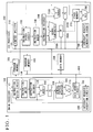
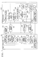
- FIG. 1 shows the structure of a microprocessor system provided in accordance with a first embodiment of the invention.
- This microprocessor system is constructed so as to be able to execute a plurality of kinds of sets of instructions described in different program languages and comprises, as its principal constituent elements, a general purpose microprocessor 100 in which a general-purpose register architecture has been employed and a co-processor 200 in which a stack architecture has been employed.
- the main processor 100 executes by means of hardware a first set of instructions for realizing program languages such as C language and an assembler and also executes by means of software a second set of instructions for realizing specific languages such as the Java language.
- the co-processor 200 operates under the control of the main processor 100 in concert therewith and executes by means of hardware the second set of instructions, for example, for the Java language, which are different from the first set of instructions.
- a program memory 300 is provided to store a program for controlling a sequence of operations of the main processor 100, i.e., a machine language corresponding to the first instruction set.
- a program memory 400 is provided to store as the second instruction set intermediate codes, for example, for a Java virtual machine.
- a data memory 500 is provided for storing data to be handled by the main processor 100 such as arithmetic data to be input to the main processor 100 and the results of such arithmetic operations.
- the program memory 300 is directly connected to the main processor 100.
- the program memory 400 and the data memory 500 are connected, through an external bus 600 (a data bus disposed externally of the main processor 100 and the co-processor 200), to each other and to the main processor 100.
- the main processor 100, the co-processor 200, the program memories 300 and 400, the data memory 500 and the external bus 600 are mounted on the same print circuit board to constitute the microprocessor system. Alternatively, some or all of these elements can be integrated in a single system LSI (Large Scale Integration).
- the main processor 100 has the following structure to form a circuitry for decoding the second set of instructions to thereby control the progress of a program.
- the main processor 100 comprises an instruction fetch circuit 110 for accessing the program memory 300 to fetch therefrom an instruction belonging to the first instruction set (hereinafter referred to simply as "first instruction"), an instruction queue 120 for temporarily holding the first instruction thus fetched, an instruction decoder 130 for decoding the first instruction, an adder 140 for updating the address of the instruction currently processed by the main processor 100 (i.e., the value in a program counter which will hereinafter be referred to as "PC value”) and the program counter 150 for holding the PC value.
- first instruction an instruction fetch circuit 110 for accessing the program memory 300 to fetch therefrom an instruction belonging to the first instruction set (hereinafter referred to simply as "first instruction")
- an instruction queue 120 for temporarily holding the first instruction thus fetched
- an instruction decoder 130 for decoding the first instruction
- an adder 140 for updating the address of the instruction currently processed by the main processor 100 (
- the main processor 100 further has the following structure to form a circuitry for carrying out an operation in accordance with the result of the decoding by the instruction decoder 130.
- the main processor 100 comprises a general purpose register 160 for temporarily holding input data to be used in an arithmetic operation, the results of such operation (output data) and the like; an arithmetic logic unit 170 for performing an arithmetic operation on the input data (hereinafter referred to as "ALU"); a data access circuit 180 for causing data to be loaded or stored between the general purpose register 160 and the external bus 600 using an address as produced by the ALU 170; and an interrupt request reception circuit 190 for receiving an interrupt request fed from the co-processor 200 which will be described later.
- ALU arithmetic logic unit
- This general-purpose main processor 100 is arranged such that it can indirectly execute the second set of instructions by means of software by executing the first set of instructions by hardware.
- the co-processor 200 When the co-processor 200 encounters any of those specific ones of the second set of instructions for which the co-processor 200 has to process data which is under the control of the main processor 100, the co-processor 200 informs the main processor 100 that it requests the main processor to execute this instruction. More specifically, the co-processor 200 has the following structure to form a circuitry for decoding the second set of instructions contained in a program to thereby control the progress of the program.
- the co-processor 200 comprises a control register 210 for temporarily holding control data for controlling its own specific basic operations (for example, data for commanding the start of operation or the stop of operation), an instruction fetch circuit 220 for fetching from the program memory 400 an instruction belonging to the second instruction set (hereinafter referred to simply as "second instruction") in accordance with the control data held in the control register 210, an instruction queue 230 for temporarily holding the second instruction thus fetched, an instruction decoder 240 for decoding the fetched second instruction, an adder-subtracter 250A for updating the top address of stacked data (i.e., the value in a stack pointer, which will hereinafter be referred to as "SP value”) under the command of the instruction decoder, the stack pointer 260A for holding the SP value, an adder 250B for updating an address of the currently processed instruction (i.e., a program count value, which will hereinafter be referred to as "PC value”) under the command of the instruction decoder 240 and a program counter 260
- top address of the stacked data or "SP value" in this invention should be understood to mean an address of the most recent data stacked.
- the co-processor 200 further has the following structure to form a circuitry for carrying out an operation in accordance with the results of decoding by the instruction decoder 240.
- the co-processor 200 comprises a stack memory 270 for retaining various data (arithmetic operands, local variables, procedural operands and so on of the second instruction) generated in the course of executing the second instruction, an ALU 280 for performing an arithmetic operation on the operand in the stack memory 270 and an interrupt request generation circuit 290 for generating an interrupt request to the main processor 100 in accordance with the result of decoding by the instruction decoder 240.
- the stack built in the stack memory 270 grows from the lower address side to the higher address side, and the width of each stack data contained in the stack is selected to be thirty-two bits (four bytes) for example.
- control register 210 the stack pointer 260A, the program counter 260B, and the stack memory 270 are connected to the external bus 600 through an internal bus 201 of the co-processor 200.
- the contents of the control register 210 and the stack pointer 260A in the co-processor 200 can be set directly by the main processor 100.
- the stack memory 270 is a memory of the LIFO (Last In First Out) type and temporarily retains data during the execution of a program by stacking them one upon the other.
- the example of FIGS. 2A and 2B shows how the contents of the stack memory are changed when a binomial operation is performed on two pieces of data contained respectively in the top address indicated by the stack pointer and its preceding address (an address obtained by subtracting four).
- data D1 to D5 are sequentially loaded in addresses "0x1004" to "0x1014" in a stacked manner ("0x” signifies a hexadecimal number) as shown in FIG. 2A.
- the address "0x1014" of the last loaded data D5 is the stack top address and corresponds to the value in the stack pointer.
- the data D4 and the data D5 are added together to form an operation result.
- the data D4 and D5 will not be necessary any longer. Therefore, as shown in FIG. 2B, the data D6 thus calculated as the operation result is stored in the address "0x1010" next to the address of the following data D3 and the value in the stack pointer is updated to indicate the address "0x1010".
- the stack memory temporarily stores data in the course of processing an operation and the stack pointer indicates the top address of the data effective at that time.
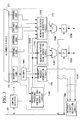
- FIG. 3 shows the detailed structure of the instruction decoder 240 together with its peripheral circuits.
- An alignment circuit 221 is constructed as a part of the function of the instruction fetch circuit 220 and serves to extract an operation code and operands from the fetched second instruction and to output them to the instruction queue 230 after aligning them.
- the instruction decoder 240 is constituted comprising a decoder 240A for decoding the operation code held in the instruction queue 230, a processing procedure control signal generation circuit 240B for generating a processing procedure control signal S240B in accordance with the decoding result of the operation code, an SP increase/decrease value generation circuit 240C for generating an increase/decrease value for the SP value and a PC increase/decrease value generation circuit 240D for generating an increase/decrease value for the PC value.
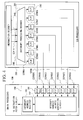
- FIG. 4 shows in more detail the interrupt request reception circuit 190 in the main processor 100 and the interrupt request generation circuit 290 in the co-processor 200.
- the interrupt request generation circuit 290 is comprised of an interrupt processing decoder 291 and a plurality of flip-flops (F/F) 292.
- the interrupt processing decoder 291 outputs an interrupt vector S290 composed of a plurality of dedicated interrupt request signals S290A to S290F and a common interrupt request signal S290G in accordance with an interrupt request signal S241A from the instruction decoder 240.
- the plurality of dedicated interrupts request signals S290A to S290F will be referred to as "dedicated interrupt vector" according to circumstances.
- the dedicated interrupt request signals S290A to S290F have been assigned in advance to a specific one or ones of the second set of instructions which the co-processor cannot process by itself and which have a relatively high frequency of execution. That is to say, when the co-processor encounters any of these specific instructions, that dedicated interrupt request signal that has been assigned to this encountered instruction is activated. Thus, the main processor can recognize the encountered instruction directly from the activated dedicated interrupt request signal.
- the common interrupt request signal S290G has been assigned in common to those instructions, other than the above-described specific instructions, which the co-processor cannot process by itself.
- the co-processor 200 is thus arranged so as to issue a "notification" by means of the one or the plurality of dedicated interrupt request signals assigned in advance to the one or the plurality of instructions of the second set of instructions having a high frequency of execution.
- the determination of whether the co-processor 200 can process an instruction by itself is made based on whether it becomes necessary in the course of processing (or executing) the instruction to operate the data which is under the control of the main processor 100 (for example, the data contained in the data memory 500). That is to say, the co-processor 200 determines in such a manner that those instruction for which data under the control of the main processor 100 must be operated cannot be processed by itself and that other instructions can be processed by itself.
- the specific instructions which the co-processor 200 cannot process by itself have been defined in advance in the instruction decoder 240.
- the dedicated interrupt request signals S290A to S290F and the common interrupt request signal S290G are held in the flip-flops 292 and then outputted as the interrupt vector S290 to the main processor 100.
- the second instruction is identified by a logical combination of the three kinds of interrupt request signals S241A fed from the instruction decoder 240, and one of the dedicated interrupt request signals S290A to S290F and the common interrupt request signal S290G is selectively activated in accordance with the content of the instruction thus identified.
- the dedicated interrupt request signals S290A to S290F may be given priorities.
- a single instruction may be assigned to an interrupt request signal of a higher priority while a plurality of instructions may be assigned to an interrupt request signal of a lower priority.
- a dedicated handler can immediately be specified for an instruction to which an interrupt request signal of a higher priority has been assigned.
- a routine for processing the interrupt by this instruction is specified.
- the interrupt request reception circuit 190 in the main processor 100 is comprised of a plurality of flip-flops 191, an interrupt handler address generation circuit 192 and an interrupt address register 193.
- the dedicated interrupt request signals S290A to S290F and the common interrupt request signal S290G sent from the co-processor are held respectively by the plurality of flip-flops 191.
- the interrupt handler address generation circuit 192 encodes the dedicated interrupt request signals S290A to S290F from the co-processor 200 to generate the address of an interrupt handler. This address of the interrupt handler is held in the interrupt address register 193 and then outputted to the above-described instruction fetch circuit 110.
- the interrupt request reception circuit 190 is thus arranged to encode the dedicated interrupt request signals (dedicated interrupt vectors) from the co-processor 200 to specify an interrupt handler which corresponds to the specific instruction to be processed.
- the main processor 100 performs various kinds of operations with respect to the co-processor 200 to control the operation thereof. These operations are performed by means of software by executing programs stored in the program memory 300 with the main processor 100.
- the second instruction, which the co-processor 200 thus encountered is an instruction for which it is not necessary to operate any data under the control of the main processor such as "iadd" for a Java virtual machine (an instruction to add integer number data together), i.e., an instruction which the co-processor 200 can process (which corresponds to "YES" at step ST15), the co-processor 200 executes the following steps ST16 to ST19 in order to process this instruction.
- the SP increase/decrease value generation circuit 240C calculates an increase/decrease value for the current SP value in accordance with the result of decoding by the decoder 240A in the instruction decoder 240.
- the adder-subtracter 250A adds the calculated increase/decrease value to the current SP value to update the SP value and sets this updated SP value to the stack pointer 260A.
- the PC increase/decrease value generation circuit 240D calculates an increase/decrease value for the current PC value in accordance with the result of decoding by the decoder 240A in the instruction decoder 240.
- the adder 250B adds the calculated increase/decrease value to the current PC value to update the PC value and sets this updated PC value to the program counter 260B.
- the PC and SP values are updated by adding "1" to the current PC value in the program counter 260B and by subtracting "4" from the current SP value in the stack pointer 260A.
- the co-processor 200 makes a negative determination at the step ST15 ("NO" at step ST15).
- each of the following steps ST20 to ST26 is executed by the main processor 100 or the co-processor 200 in order to process this instruction.
- the co-processor 200 takes a negative determination at the above-described step ST20 ("NO" at step ST20). In this case, a notification will be made by means of the common interrupt request signal S290G, but it will not be possible to identify in a univocal manner the kind of the instruction from this interrupt request signal S290G which is common to a plurality of instructions. Therefore, the main processor 100 and the co-processor 200 execute the following steps ST30 to ST34 and ST24 to ST26 to identify the instruction and process the identified instruction.
- the co-processor 200 itself determines whether it can process the fetched instruction by itself.
- the operation of this instruction is executed by the main processor 100 with its software while the updating process of the PC and SP values which will take place as a result of the execution of the instruction is carried out by the co-processor 200 with its hardware.
- the main processor 100 does not need to perform the updating process of the PC and SP values when it processes with its software the instruction which was requested to execute by the co-processor 200, so that the load on the processing by means of software in the main processor 100 can be decreased.
- the co-processor 200 when the co-processor 200 encounters an instruction which it cannot process by itself, it signals the main processor 100 of this fact with an interrupt vector which has been assigned exclusively to this instruction. With this arrangement, the main processor 100 can know the kind of the instruction directly from the interrupt vector. Thus, the load on the processing by means of software when specifying the interrupt handler can be decreased.
- each of the dedicated interrupt signals S290A to S290F has been assigned in advance to a respective one of the plurality of specific instructions which the co-processor 200 cannot process by itself and which have a relatively high frequency of execution.
- the invention should not be restricted to such arrangement only, but a single dedicated interrupt request signal can be assigned to two or more instructions.
- the main processor 100 may carry out the processing for identifying the kind of instruction (steps ST31 to ST34) by reading the PC value of the program counter from the co-processor 200 in a manner described above for the case where an interrupt request was made with the common interrupt request signal S290G.
- the dedicated interrupt request signals can be assigned to much more instructions although it becomes necessary to carry out the processing for identifying the instruction from the PC value.
- the instructions which the co-processor 200 cannot process by itself have been assumed, by way of example, to be those instructions for which data under the control of the main processor need to be handled.
- the present invention should not be restricted only to such arrangement.
- the co-processor may request the main processor 100 to execute that instruction.
- Examples of such instruction may include, in addition to those instructions involving the operation of the data which is under the control of the main processor, instructions for which an exchange of stack frames (sets of stack data defined in a program) will take place and instructions each for executing a floating-point arithmetic operation.
- co-processor 200 executes those instructions which can be processed by a RISC (Reduced Instruction Set Computer) type processor employing a stack architecture while the main processor 100 executes the other instructions which need more complicated processing, to thereby separate the instructions to be processed by the main processor 100 from those to be processed by the co-processor 200.
- RISC Reduced Instruction Set Computer
- the incorporated stack memory 270 cannot secure a sufficient storage capacity on the chip of the semiconductor integrated circuit due to its limited size. In such case, it will be necessary to provide a hardware means or a software means for detecting an overflow or an underflow of the data written into the stack memory 270.
- a register storing the upper-limit and the lower-limit address that the stack pointer 260A can take may be provided, for example.
- an overflow and an underflow of the data can be detected by comparing the value of the stack pointer with the value in this register each time the value of the stack pointer is updated.
- Notification of the detection to the main processor 100 can be made by generating an interrupt similarly to the case where a non-executable instruction is encountered or by changing a specific bit of the control register 210.
- the amount of data used in the stack i.e., the size of the stack frame is specified in advance in the file, in which an intermediate code called a byte code is stored, for each unit of execution of individual programs. In such case, this can be checked by the main processor 100 according to its software before each program is executed.
- the data in the stack memory 270 is saved in the data memory 500 by the main processor 100 according to its software.
- the data saved in the data memory 500 is restored to the stack memory 270.
- Such saving or restoration of data can be performed at once for the whole data of the stack memory 270 or can be performed one after the other for its divided portions.
- this first embodiment it can be achieved, by the integration of the high speed stack memory 270 having a limited storage capacity in the co-processor 200, that an arithmetic operation on data contained in the stack as its operand is performed by the ALU 280 at a high speed. It may also easily be possible to secure a sufficient storage capacity for avoiding an overflow from occurring by forming the data memory 500 in a semiconductor integrated circuit which is different from any of the main processor 100 and the co-processor 200.
- the top (the upper-most) four of the stack data are held in registers that are accessible at a high speed in order that instructions can be executed efficiently.
- those stack data other than the top four data need not be held in registers and can be held in an external memory (stack memory 270) without causing any trouble in executing an instruction.
- Described hereinafter is a microprocessor system provided in accordance with the second embodiment that is adapted to hold only the top four of the stack data as described above and yet suitable for processing the Java language.
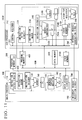
- FIG. 7 shows the structure of the microprocessor system according to this second embodiment.
- This microprocessor system comprises a co-processor 200A which includes, instead of the stack memory 270 provided in the above-described microprocessor system according to the first embodiment (FIG. 1), a stack-top register 270A and a stack memory 270B.
- the instruction queue 230 is also connected to the internal bus 201 so that the main processor 100 can directly read the contents of the instruction queue 230.
- the stack-top register 270A is connected to the ALU 280 and holds the top four data (a predetermined number of data, in general) among the stack data.
- This stack-top register 270A is constructed so that it can perform read and write operations simultaneously at a high speed.
- the stack memory 270B corresponds to the stack memory 270 in the above-described first embodiment and is provided outside the co-processor 200A.
- This stack memory 270B is connected to the external bus 600 and to the stack-top register 270A and holds the lower-order data of the stack data except for the top four data.
- the SP value in the stack pointer 260A indicates the top address of the stack memory 270B.
- FIGS. 8A and 8B The description of the general operation of the stack-top register and the stack memory will be supplemented with reference to FIGS. 8A and 8B.
- the stack-top register holds the top two data in FIGS. 8A and 8B.
- Each of the stack-top register and the stack memory writes and reads data in a LIFO method similarly to the above-described stack memory 270.
- the top two data D14 and D15 of the stack data D11 to D15 are held in the stack-top register.
- FIGS. 8A and 8B shows, by way of example, how the contents of the stack-top register and the stack memory are changed when a binominal operation is performed.
- data D 11 to D15 are sequentially loaded in addresses "0x1004" to "0x1014" in a stacked manner as shown in FIG. 8A.
- the address "0x100C" of the data D13 which was loaded last in the stack memory is the top address of the stack memory and, at the same time, corresponds to the value of the stack pointer.
- a binominal operation a binominal adding operation, for example
- the data D14 and the data D15 are added together, because of which the data D16 is obtained.
- the data D14 and D15 will not be necessary any longer, and the addresses "0x1010" and "0x1014" become empty. Therefore, the data D16 thus obtained as the operation result is stored in the lower-order one of the emptied addresses, i.e., the address "0x1010" which is next to the succeeding data D13.
- the two data namely, the top data D16 and its succeeding data D13, are held in the stack-top register. In this manner, during the process of an operation a predetermined number of data of the stack data are temporarily retained in the stack-top register.
- the top two data are held in the stack-top register
- the top four data are held in the stack-top register 270A according to the structure of the second embodiment (FIG. 7).
- the present invention should not be restricted to such number, but the number of data held in the stack-top register 270A may be set to any number as occasion demands.
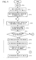
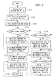
- this second embodiment including the operation for exchanging stack frames (sets of stack data as defined in a program) will now described with reference to the flow chart shown in FIG. 9.
- the operation of various portions is initialized by resetting this microprocessor system. After this resetting, the main processor 100 starts its operation while the co-processor 200A is held in a stop state.
- the stack memory 270B now stores, in addition to the argument data D21 to the argument data D25, the local variable D26 and a part of the context D27 (context d27-n) as new data.
- the stack-top register 270A stores the remaining parts of the context D27 (context d27-1 and d27-2). The sequence of processing steps for changing the stack frame is carried out by the main processor 100 according to its software.
- the value of the stack pointer significantly changes when a change of stack frame is performed.
- the processing to be carried out in the main processor 100 becomes substantially complex.
- the determination in this step is made for determining whether such a space must be reserved prior to the execution of the operation.
- the stack decreases, it will not be allowed to decrease the stack pointer before the execution of the operation. This is because if the stack pointer is decreased it may happen that data necessary for the operation could be invalidated.
- step ST109 in which the PC value of the program counter 260B is updated. Then, the processing returns to the step ST103 to process the next instruction.
- the co-processor 200A writes all the stack data of the stack-top register 270A into the stack memory 270B before notifying the main processor 100 and reads the top data from the stack memory 270B into the stack-top register 270A after the processing by the main processor 100 is complete and the operation of the co-processor resumes.
- the main processor 100 can handle the stack data in the interrupt handler in a single memory space, so that the processing for handling the data in the stack-top register 270A is simplified.
- instructions of those program languages such as the Java language that have affinity to the architecture including the stack-top register 270A can be executed efficiently.
- the storage capacity of the stack memory 270B can also be increased since the stack memory 270B is provided outside the co-processor 200A. Nevertheless, the stack memory 270B may be provided inside the co-processor 200A if it is feasible.
- FIG. 11 shows the structure of a microprocessor system provided in accordance with this third embodiment.
- This microprocessor system is different from the above-described second embodiment (FIG. 7) in that it comprises a co-processor 200B which includes a cache memory 270C between the stack-top register 270A and the stack memory 270B.
- This cache memory 270C is provided for caching a part of the data retained in the stack memory 270B.
- the stack memory 270B is separated from the external bus 600.
- the cache memory 270C By the provision of the cache memory 270C, it is apparently achieved that the external stack memory 270B is accessed at a high speed, with the result that the processing is accelerated. In this case, the stack memory 270B must be accessed through the cache memory 270C in order to maintain the concordance of data between the stack memory 270B and the cache memory 270C. For that purpose, the stack memory 270B is separated from the external bus 600 so that the stack memory 270B cannot directly be accessed by the external bus 600.
- the main processor 100 in order to access data contained in the stack memory 270B the main processor 100 must gain such an access through the external bus 600 and the internal bus 201 of the co-processor 200B and further through the cache memory 270C.
- a high-speed access to the stack memory 270B can be achieved since the stack memory 270B is accessed through the cache memory 270C. That is to say, even if the stack memory 270B is of the type that a high speed accessing is impossible, the apparent processing therefor can be accelerated.
- the storage capacity of the stack memory 270B can be increased since the stack memory 270B is located externally of the co-processor 200B.
- this third embodiment it will not be necessary to take any measure against an overflow if the storage capacity of the externally connected stack memory 270B is made a large, since the cache memory 270C itself has a function of controlling data to be cached. That is to say, although an overflow or an underflow is detected in the first embodiment by hardware or a software means, this third embodiment does not need an overflow detection means or an underflow detection means. In addition, since no exchange of memory will be needed when an overflow or an underflow is detected, the chip size as well as the size of program code for the control software can be decreased.
- FIG. 12 shows the structure of a microprocessor system provided in accordance with this fourth embodiment.
- This processor system comprises a plurality of coprocessors (three co-processors in this case) 200X, 200Y and 200Z with respect to the single main processor 100.
- the co-processors 200X, 200Y, and 200Z comprise dedicated stack memories 270XM, 270YM and 270ZM, respectively, each of which corresponds to the stack memory 270 of the above described first embodiment.
- the co-processors 200X, 200Y, and 200Z are connected to the main processor 100 through the external bus 600 and to the program memory 400 through an external bus 600B.
- the program memory 400 and the data memory 500 are connected to the main processor 100 through the external bus 600.
- Interrupt requests S290H from the respective co-processors are directly inputted to the main processor 100.
- each of the stack memories 270XM, 270YM and 270ZM of the co-processors is local data (for example, local variable, local arithmetic data and local working data) specific to a respective one of the co-processors.
- local data for example, local variable, local arithmetic data and local working data
- a set of data corresponding to a "thread" which is a unit of task described in a program is stored as the local data.
- the determination of whether a given instruction is an instruction to be processed by the main processor 100 or an instruction to be processed by any of the co-processors 200X, 200Y and 200Z is made based on whether a heap area (i.e., an area in which an object is written) provided in the data memory 500 has to be manipulated or not. That is to say, an instruction that needs manipulation of the heap area is processed by the main processor 100, while an instruction that needs no manipulation of the heap area is processed by the co-processor 200X, 200Y, and 200Z.
- a heap area i.e., an area in which an object is written
- the main processor 100 When threads, which two or more of the co-processors execute, access an object formed in a heap area in the data memory 500, the main processor 100 carries out an exclusive control among the respective threads.
- each of the co-processors processes only those instructions that it can execute by itself by accessing a respective one of the stack memories 270XM, 270YM and 270ZM in which specific local data are contained.
- the main processor 100 processes those instructions that involve coordination among the co-processors. For example, an "invokevirtual" instruction as defined in the Java virtual machine selectively executes a specific process in a program in which a plurality of processes are described with respect to an object in a heap area. In this case, when the object to be processed is being used exclusively by another thread, the execution of the program must be waited for until the use is terminated.
- the main processor 100 waits for the end of the thread under execution and then accesses the co-processor, from which the next request was received, to set the address in which the process to be executed is described to the program counter and thereafter sets the control register of the relevant co-processor to the "start of operation" state.
- a "Garbage Collection" instruction of the Java language i.e., a process for operating an object in a heap area to remove data which is not necessary any longer, is executed by the main processor 100 irrespective of any interrupt from the co-processors.
- the main processor 100 is arranged to mask these interrupts in advance. With this arrangement, it can be avoided that an object whose storage location has been moved due to the "Garbage Collection” is rewritten.
- a multiple of tasks can be processed by the plurality of co-processors 200X, 200Y and 200Z, so that those programs such as the Java language which have the concept of multi-thread can be executed at a high speed.
- the processing time of the microprocessor system as a whole can significantly be reduced since the main processor 100 can carry out processes such as the "Garbage Collection" in parallel with the processing in each of the co-processors.
- the main processor 100 can easily control the requests for operating objects by masking interrupts from the respective co-processors.
- a "Garbage Collection" can be performed easily and in real time.
- various notifications to the main processor are made by means of interrupts from the co-processor to the main processor.
- the present invention should not be restricted to such a structure only, but the main processor may recognize the fact that the co-processor encounters a specific instruction which it cannot execute by itself, by providing in the co-processor a status register in which data for notifying an interrupt request is written and by periodically accessing this status register by the main processor (i.e., by a so-called polling). With this arrangement, the "notification" is eventually transmitted to the main processor that executes the corresponding process in response thereto.
- the present invention can be regarded as an invention in which the manner of processing an instruction that the co-processor encounters is selected in accordance with the contents of that instruction, when viewed from another angle.
- the subject which carries out the processing is selected in such a manner that those instructions which can be processed only with the stack data which the co-processor has are processed by the co-processor itself, while those instructions which needs a manipulation of a heap area in the data memory as well as those instructions which needs a modification of the stack frame are processed by the main processor.
Landscapes
- Engineering & Computer Science (AREA)
- Software Systems (AREA)
- Theoretical Computer Science (AREA)
- Physics & Mathematics (AREA)
- General Engineering & Computer Science (AREA)
- General Physics & Mathematics (AREA)
- Advance Control (AREA)
- Multi Processors (AREA)
- Executing Machine-Instructions (AREA)
Applications Claiming Priority (2)
| Application Number | Priority Date | Filing Date | Title |
|---|---|---|---|
| JP33196099A JP3621315B2 (ja) | 1999-11-22 | 1999-11-22 | マイクロプロセッサシステム |
| JP33196099 | 1999-11-22 |
Publications (2)
| Publication Number | Publication Date |
|---|---|
| EP1102164A2 true EP1102164A2 (fr) | 2001-05-23 |
| EP1102164A3 EP1102164A3 (fr) | 2002-09-04 |
Family
ID=18249578
Family Applications (1)
| Application Number | Title | Priority Date | Filing Date |
|---|---|---|---|
| EP00125496A Withdrawn EP1102164A3 (fr) | 1999-11-22 | 2000-11-21 | Système de microprocesseur |
Country Status (3)
| Country | Link |
|---|---|
| US (1) | US7200741B1 (fr) |
| EP (1) | EP1102164A3 (fr) |
| JP (1) | JP3621315B2 (fr) |
Cited By (3)
| Publication number | Priority date | Publication date | Assignee | Title |
|---|---|---|---|---|
| EP1146421A3 (fr) * | 2000-04-12 | 2001-10-24 | Sony Corporation | Procédé de commande et dispositif électronique pour renforcer la fonctionnalité d'un processeur principal |
| GB2367652A (en) * | 2000-10-05 | 2002-04-10 | Advanced Risc Mach Ltd | Scheduling control within a system having mixed hardware and software based instruction execution |
| TWI419048B (zh) * | 2006-03-24 | 2013-12-11 | Ericsson Telefon Ab L M | 具有位址產生器之處理器 |
Families Citing this family (45)
| Publication number | Priority date | Publication date | Assignee | Title |
|---|---|---|---|---|
| JP3561506B2 (ja) * | 2001-05-10 | 2004-09-02 | 東京エレクトロンデバイス株式会社 | 演算システム |
| JP4717291B2 (ja) * | 2001-09-13 | 2011-07-06 | ルネサスエレクトロニクス株式会社 | 制御レジスタ及びプロセッサ |
| EP1387259B1 (fr) * | 2002-07-31 | 2017-09-20 | Texas Instruments Incorporated | Controle interprocesseur |
| GB0415851D0 (en) * | 2004-07-15 | 2004-08-18 | Imagination Tech Ltd | Microprocessor output ports and control of instructions provided therefrom |
| US7752427B2 (en) * | 2005-12-09 | 2010-07-06 | Atmel Corporation | Stack underflow debug with sticky base |
| US8914618B2 (en) | 2005-12-29 | 2014-12-16 | Intel Corporation | Instruction set architecture-based inter-sequencer communications with a heterogeneous resource |
| KR100781340B1 (ko) * | 2006-09-18 | 2007-11-30 | 삼성전자주식회사 | 사용자 정의 확장 연산을 처리하는 연산 시스템 및 방법 |
| US7797514B2 (en) * | 2006-11-16 | 2010-09-14 | Texas Instruments Incorporated | Scalable multi-threaded sequencing/synchronizing processor architecture |
| JP4751814B2 (ja) * | 2006-11-28 | 2011-08-17 | 富士通東芝モバイルコミュニケーションズ株式会社 | 携帯端末 |
| US8006068B1 (en) * | 2007-04-18 | 2011-08-23 | Xilinx, Inc. | Processor access to data cache with fixed or low variable latency via instructions to an auxiliary processing unit |
| US7840703B2 (en) * | 2007-08-27 | 2010-11-23 | International Business Machines Corporation | System and method for dynamically supporting indirect routing within a multi-tiered full-graph interconnect architecture |
| US7958182B2 (en) | 2007-08-27 | 2011-06-07 | International Business Machines Corporation | Providing full hardware support of collective operations in a multi-tiered full-graph interconnect architecture |
| US8014387B2 (en) * | 2007-08-27 | 2011-09-06 | International Business Machines Corporation | Providing a fully non-blocking switch in a supernode of a multi-tiered full-graph interconnect architecture |
| US8140731B2 (en) | 2007-08-27 | 2012-03-20 | International Business Machines Corporation | System for data processing using a multi-tiered full-graph interconnect architecture |
| US7822889B2 (en) * | 2007-08-27 | 2010-10-26 | International Business Machines Corporation | Direct/indirect transmission of information using a multi-tiered full-graph interconnect architecture |
| US7769891B2 (en) * | 2007-08-27 | 2010-08-03 | International Business Machines Corporation | System and method for providing multiple redundant direct routes between supernodes of a multi-tiered full-graph interconnect architecture |
| US7958183B2 (en) | 2007-08-27 | 2011-06-07 | International Business Machines Corporation | Performing collective operations using software setup and partial software execution at leaf nodes in a multi-tiered full-graph interconnect architecture |
| US7793158B2 (en) * | 2007-08-27 | 2010-09-07 | International Business Machines Corporation | Providing reliability of communication between supernodes of a multi-tiered full-graph interconnect architecture |
| US7809970B2 (en) * | 2007-08-27 | 2010-10-05 | International Business Machines Corporation | System and method for providing a high-speed message passing interface for barrier operations in a multi-tiered full-graph interconnect architecture |
| US8185896B2 (en) | 2007-08-27 | 2012-05-22 | International Business Machines Corporation | Method for data processing using a multi-tiered full-graph interconnect architecture |
| US8108545B2 (en) | 2007-08-27 | 2012-01-31 | International Business Machines Corporation | Packet coalescing in virtual channels of a data processing system in a multi-tiered full-graph interconnect architecture |
| US7769892B2 (en) | 2007-08-27 | 2010-08-03 | International Business Machines Corporation | System and method for handling indirect routing of information between supernodes of a multi-tiered full-graph interconnect architecture |
| US7904590B2 (en) | 2007-08-27 | 2011-03-08 | International Business Machines Corporation | Routing information through a data processing system implementing a multi-tiered full-graph interconnect architecture |
| US7827428B2 (en) | 2007-08-31 | 2010-11-02 | International Business Machines Corporation | System for providing a cluster-wide system clock in a multi-tiered full-graph interconnect architecture |
| US7921316B2 (en) | 2007-09-11 | 2011-04-05 | International Business Machines Corporation | Cluster-wide system clock in a multi-tiered full-graph interconnect architecture |
| US8359462B1 (en) * | 2007-11-21 | 2013-01-22 | Marvell International Ltd. | Method and apparatus for programmable coupling between CPU and co-processor |
| US7779148B2 (en) | 2008-02-01 | 2010-08-17 | International Business Machines Corporation | Dynamic routing based on information of not responded active source requests quantity received in broadcast heartbeat signal and stored in local data structure for other processor chips |
| US8077602B2 (en) * | 2008-02-01 | 2011-12-13 | International Business Machines Corporation | Performing dynamic request routing based on broadcast queue depths |
| US20090198956A1 (en) * | 2008-02-01 | 2009-08-06 | Arimilli Lakshminarayana B | System and Method for Data Processing Using a Low-Cost Two-Tier Full-Graph Interconnect Architecture |
| GB0816319D0 (en) * | 2008-09-05 | 2008-10-15 | Palmer Charles G | Network communication |
| US8417778B2 (en) * | 2009-12-17 | 2013-04-09 | International Business Machines Corporation | Collective acceleration unit tree flow control and retransmit |
| US8407444B2 (en) * | 2009-12-23 | 2013-03-26 | International Business Machines Corporation | Hardware off-load garbage collection acceleration for languages with finalizers |
| US8943108B2 (en) * | 2009-12-23 | 2015-01-27 | International Business Machines Corporation | Hardware off-load memory garbage collection acceleration |
| JP5555514B2 (ja) * | 2010-03-17 | 2014-07-23 | ルネサスエレクトロニクス株式会社 | プロセッサシステム |
| US8751655B2 (en) | 2010-03-29 | 2014-06-10 | International Business Machines Corporation | Collective acceleration unit tree structure |
| JPWO2012035699A1 (ja) * | 2010-09-15 | 2014-01-20 | 日本電気株式会社 | 情報処理装置、情報処理方法、設計支援システム、及びプログラム |
| US8677050B2 (en) * | 2010-11-12 | 2014-03-18 | International Business Machines Corporation | System, method and computer program product for extending a cache using processor registers |
| EP2764455B1 (fr) | 2011-10-05 | 2022-04-20 | Opteon Corporation | Système et procédé pour la surveillance et/ou le contrôle d'environnements dynamiques |
| US9417873B2 (en) | 2012-12-28 | 2016-08-16 | Intel Corporation | Apparatus and method for a hybrid latency-throughput processor |
| US10140129B2 (en) | 2012-12-28 | 2018-11-27 | Intel Corporation | Processing core having shared front end unit |
| US9542193B2 (en) | 2012-12-28 | 2017-01-10 | Intel Corporation | Memory address collision detection of ordered parallel threads with bloom filters |
| US9361116B2 (en) * | 2012-12-28 | 2016-06-07 | Intel Corporation | Apparatus and method for low-latency invocation of accelerators |
| US10346195B2 (en) | 2012-12-29 | 2019-07-09 | Intel Corporation | Apparatus and method for invocation of a multi threaded accelerator |
| US9817670B2 (en) | 2013-12-13 | 2017-11-14 | International Business Machines Corporation | Framework to provide time bound execution of co-processor commands |
| US10838893B2 (en) * | 2014-05-30 | 2020-11-17 | Apple Inc. | Methods for mitigating system interrupts for an electronic device |
Family Cites Families (15)
| Publication number | Priority date | Publication date | Assignee | Title |
|---|---|---|---|---|
| DE2546202A1 (de) * | 1975-10-15 | 1977-04-28 | Siemens Ag | Rechnersystem aus mehreren miteinander verbundenen und zusammenwirkenden einzelrechnern und verfahren zum betrieb des rechnersystems |
| US4870614A (en) | 1984-08-02 | 1989-09-26 | Quatse Jesse T | Programmable controller ("PC") with co-processing architecture |
| DE3538214C2 (de) * | 1984-10-30 | 1994-06-16 | Mitsubishi Electric Corp | Multiprozessorsystem |
| US4695945A (en) * | 1985-02-28 | 1987-09-22 | International Business Machines Corporation | Processor I/O and interrupt filters allowing a co-processor to run software unknown to the main processor |
| US4860200A (en) * | 1985-07-03 | 1989-08-22 | Tektronix, Inc. | Microprocessor interface device for coupling non-compatible protocol peripheral with processor |
| JPH0687221B2 (ja) | 1986-04-02 | 1994-11-02 | 日本電気株式会社 | 情報処理装置 |
| US5109514A (en) * | 1988-07-28 | 1992-04-28 | Sun Microsystems, Inc. | Method and apparatus for executing concurrent CO processor operations and precisely handling related exceptions |
| JPH02311948A (ja) | 1989-05-26 | 1990-12-27 | Nec Corp | コプロセッサの誤り修正方式 |
| US5768613A (en) * | 1990-07-06 | 1998-06-16 | Advanced Micro Devices, Inc. | Computing apparatus configured for partitioned processing |
| JP2908096B2 (ja) | 1992-01-22 | 1999-06-21 | 富士通株式会社 | コプロセッサ制御方式 |
| JP3451595B2 (ja) | 1995-06-07 | 2003-09-29 | インターナショナル・ビジネス・マシーンズ・コーポレーション | 二つの別個の命令セット・アーキテクチャへの拡張をサポートすることができるアーキテクチャ・モード制御を備えたマイクロプロセッサ |
| US5727227A (en) * | 1995-11-20 | 1998-03-10 | Advanced Micro Devices | Interrupt coprocessor configured to process interrupts in a computer system |
| US5715439A (en) * | 1996-12-09 | 1998-02-03 | Allen-Bradley Company, Inc. | Bi-directional co-processor interface |
| US6021273A (en) | 1997-06-30 | 2000-02-01 | Sun Microsystems, Inc. | Interpreter generation and implementation utilizing interpreter states and register caching |
| US5923892A (en) * | 1997-10-27 | 1999-07-13 | Levy; Paul S. | Host processor and coprocessor arrangement for processing platform-independent code |
-
1999
- 1999-11-22 JP JP33196099A patent/JP3621315B2/ja not_active Expired - Fee Related
-
2000
- 2000-11-21 EP EP00125496A patent/EP1102164A3/fr not_active Withdrawn
- 2000-11-21 US US09/716,378 patent/US7200741B1/en not_active Expired - Fee Related
Cited By (5)
| Publication number | Priority date | Publication date | Assignee | Title |
|---|---|---|---|---|
| EP1146421A3 (fr) * | 2000-04-12 | 2001-10-24 | Sony Corporation | Procédé de commande et dispositif électronique pour renforcer la fonctionnalité d'un processeur principal |
| US7287098B2 (en) | 2000-04-12 | 2007-10-23 | Sony Corporation | Control method and electronic device enabling recognition of functions installed in the electronic device |
| GB2367652A (en) * | 2000-10-05 | 2002-04-10 | Advanced Risc Mach Ltd | Scheduling control within a system having mixed hardware and software based instruction execution |
| GB2367652B (en) * | 2000-10-05 | 2004-08-11 | Advanced Risc Mach Ltd | Scheduling control within a system having mixed hardware and software based instruction execution |
| TWI419048B (zh) * | 2006-03-24 | 2013-12-11 | Ericsson Telefon Ab L M | 具有位址產生器之處理器 |
Also Published As
| Publication number | Publication date |
|---|---|
| JP2001147902A (ja) | 2001-05-29 |
| JP3621315B2 (ja) | 2005-02-16 |
| US7200741B1 (en) | 2007-04-03 |
| EP1102164A3 (fr) | 2002-09-04 |
Similar Documents
| Publication | Publication Date | Title |
|---|---|---|
| EP1102164A2 (fr) | Système de microprocesseur | |
| US5398330A (en) | Register file backup queue | |
| US5870582A (en) | Method and apparatus for completion of non-interruptible instructions before the instruction is dispatched | |
| US5809268A (en) | Method and system for tracking resource allocation within a processor | |
| US5043867A (en) | Exception reporting mechanism for a vector processor | |
| KR100243100B1 (ko) | 다수의 주프로세서 및 보조 프로세서를 갖는 프로세서의구조 및 보조 프로세서 공유 방법 | |
| US4949250A (en) | Method and apparatus for executing instructions for a vector processing system | |
| EP0747816A2 (fr) | Méthode et système pour opération multi-fil à haute performance dans un système de traitement de données | |
| EP1359501A2 (fr) | Dispositif de traitement pour exécuter des instructions de machine virtuelle | |
| EP0333366A2 (fr) | Méthode et dispositif de commutation de contexte pour l'utilisation dans un système de traitement de vecteurs | |
| KR100404672B1 (ko) | 슈퍼스칼라프로세서의로드버퍼와저장버퍼우선순위동적전환방법및장치 | |
| KR100368166B1 (ko) | 컴퓨터 처리 시스템에서 스택 레퍼런스를 변경하는 방법 | |
| US5930820A (en) | Data cache and method using a stack memory for storing stack data separate from cache line storage | |
| US6256725B1 (en) | Shared datapath processor utilizing stack-based and register-based storage spaces | |
| US6199156B1 (en) | System for explicitly referencing a register for its current content when performing processor context switch | |
| US20050038976A1 (en) | Processor and method for pre-fetching out-of-order instructions | |
| US7890740B2 (en) | Processor comprising a first and a second mode of operation and method of operating the same | |
| US20020144091A1 (en) | Method and apparatus for dynamic register management in a processor | |
| EP1104899A2 (fr) | Appareil de traitement de données et méthode de commande dudit appareil | |
| US12436770B1 (en) | Window-based control for instruction issue in an out-of-order processor | |
| EP0333365A2 (fr) | Méthode et dispositif pour le traitement des exceptions de gestion de mémoire asynchrones par un processeur à vecteur | |
| JPS6051947A (ja) | 仮想記憶計算機における命令先取方式 | |
| JP4631442B2 (ja) | プロセッサ | |
| JP2025151269A (ja) | キャッシュ装置およびキャッシュ装置の制御方法 | |
| US20050005086A1 (en) | Pipeline processing device and interrupt processing method |
Legal Events
| Date | Code | Title | Description |
|---|---|---|---|
| PUAI | Public reference made under article 153(3) epc to a published international application that has entered the european phase |
Free format text: ORIGINAL CODE: 0009012 |
|
| AK | Designated contracting states |
Kind code of ref document: A2 Designated state(s): AT BE CH CY DE DK ES FI FR GB GR IE IT LI LU MC NL PT SE TR |
|
| AX | Request for extension of the european patent |
Free format text: AL;LT;LV;MK;RO;SI |
|
| PUAL | Search report despatched |
Free format text: ORIGINAL CODE: 0009013 |
|
| AK | Designated contracting states |
Kind code of ref document: A3 Designated state(s): AT BE CH CY DE DK ES FI FR GB GR IE IT LI LU MC NL PT SE TR |
|
| AX | Request for extension of the european patent |
Free format text: AL;LT;LV;MK;RO;SI |
|
| 17P | Request for examination filed |
Effective date: 20020918 |
|
| RAP1 | Party data changed (applicant data changed or rights of an application transferred) |
Owner name: NEC ELECTRONICS CORPORATION |
|
| AKX | Designation fees paid |
Designated state(s): DE FR GB |
|
| 17Q | First examination report despatched |
Effective date: 20071213 |
|
| STAA | Information on the status of an ep patent application or granted ep patent |
Free format text: STATUS: THE APPLICATION HAS BEEN WITHDRAWN |
|
| 18W | Application withdrawn |
Effective date: 20080317 |