EP1102235A1 - Spannungsgenerator für Flüssigkristallanzeige mit Spannungsteiler, Differenzverstärker und Schaltkreis - Google Patents
Spannungsgenerator für Flüssigkristallanzeige mit Spannungsteiler, Differenzverstärker und Schaltkreis Download PDFInfo
- Publication number
- EP1102235A1 EP1102235A1 EP00403152A EP00403152A EP1102235A1 EP 1102235 A1 EP1102235 A1 EP 1102235A1 EP 00403152 A EP00403152 A EP 00403152A EP 00403152 A EP00403152 A EP 00403152A EP 1102235 A1 EP1102235 A1 EP 1102235A1
- Authority
- EP
- European Patent Office
- Prior art keywords
- voltage
- analog
- value
- switching
- control
- Prior art date
- Legal status (The legal status is an assumption and is not a legal conclusion. Google has not performed a legal analysis and makes no representation as to the accuracy of the status listed.)
- Withdrawn
Links
- 239000004973 liquid crystal related substance Substances 0.000 title description 4
- 230000001360 synchronised effect Effects 0.000 claims abstract description 13
- 230000000903 blocking effect Effects 0.000 claims description 3
- 230000010354 integration Effects 0.000 abstract description 3
- 230000000694 effects Effects 0.000 abstract description 2
- 230000007704 transition Effects 0.000 description 20
- 238000010586 diagram Methods 0.000 description 7
- 239000000543 intermediate Substances 0.000 description 5
- 239000013078 crystal Substances 0.000 description 2
- 230000006870 function Effects 0.000 description 2
- 239000007788 liquid Substances 0.000 description 2
- PXFBZOLANLWPMH-UHFFFAOYSA-N 16-Epiaffinine Natural products C1C(C2=CC=CC=C2N2)=C2C(=O)CC2C(=CC)CN(C)C1C2CO PXFBZOLANLWPMH-UHFFFAOYSA-N 0.000 description 1
- 230000015556 catabolic process Effects 0.000 description 1
- 230000007423 decrease Effects 0.000 description 1
- 238000006731 degradation reaction Methods 0.000 description 1
- 238000007599 discharging Methods 0.000 description 1
- 230000008030 elimination Effects 0.000 description 1
- 238000003379 elimination reaction Methods 0.000 description 1
- 238000005516 engineering process Methods 0.000 description 1
- 235000021183 entrée Nutrition 0.000 description 1
- 239000011159 matrix material Substances 0.000 description 1
- 230000001052 transient effect Effects 0.000 description 1
Images


Classifications
-
- G—PHYSICS
- G09—EDUCATION; CRYPTOGRAPHY; DISPLAY; ADVERTISING; SEALS
- G09G—ARRANGEMENTS OR CIRCUITS FOR CONTROL OF INDICATING DEVICES USING STATIC MEANS TO PRESENT VARIABLE INFORMATION
- G09G3/00—Control arrangements or circuits, of interest only in connection with visual indicators other than cathode-ray tubes
- G09G3/20—Control arrangements or circuits, of interest only in connection with visual indicators other than cathode-ray tubes for presentation of an assembly of a number of characters, e.g. a page, by composing the assembly by combination of individual elements arranged in a matrix no fixed position being assigned to or needed to be assigned to the individual characters or partial characters
- G09G3/34—Control arrangements or circuits, of interest only in connection with visual indicators other than cathode-ray tubes for presentation of an assembly of a number of characters, e.g. a page, by composing the assembly by combination of individual elements arranged in a matrix no fixed position being assigned to or needed to be assigned to the individual characters or partial characters by control of light from an independent source
- G09G3/36—Control arrangements or circuits, of interest only in connection with visual indicators other than cathode-ray tubes for presentation of an assembly of a number of characters, e.g. a page, by composing the assembly by combination of individual elements arranged in a matrix no fixed position being assigned to or needed to be assigned to the individual characters or partial characters by control of light from an independent source using liquid crystals
- G09G3/3611—Control of matrices with row and column drivers
- G09G3/3696—Generation of voltages supplied to electrode drivers
-
- G—PHYSICS
- G09—EDUCATION; CRYPTOGRAPHY; DISPLAY; ADVERTISING; SEALS
- G09G—ARRANGEMENTS OR CIRCUITS FOR CONTROL OF INDICATING DEVICES USING STATIC MEANS TO PRESENT VARIABLE INFORMATION
- G09G2310/00—Command of the display device
- G09G2310/06—Details of flat display driving waveforms
-
- G—PHYSICS
- G09—EDUCATION; CRYPTOGRAPHY; DISPLAY; ADVERTISING; SEALS
- G09G—ARRANGEMENTS OR CIRCUITS FOR CONTROL OF INDICATING DEVICES USING STATIC MEANS TO PRESENT VARIABLE INFORMATION
- G09G2330/00—Aspects of power supply; Aspects of display protection and defect management
- G09G2330/02—Details of power systems and of start or stop of display operation
- G09G2330/021—Power management, e.g. power saving
-
- G—PHYSICS
- G09—EDUCATION; CRYPTOGRAPHY; DISPLAY; ADVERTISING; SEALS
- G09G—ARRANGEMENTS OR CIRCUITS FOR CONTROL OF INDICATING DEVICES USING STATIC MEANS TO PRESENT VARIABLE INFORMATION
- G09G3/00—Control arrangements or circuits, of interest only in connection with visual indicators other than cathode-ray tubes
- G09G3/20—Control arrangements or circuits, of interest only in connection with visual indicators other than cathode-ray tubes for presentation of an assembly of a number of characters, e.g. a page, by composing the assembly by combination of individual elements arranged in a matrix no fixed position being assigned to or needed to be assigned to the individual characters or partial characters
- G09G3/34—Control arrangements or circuits, of interest only in connection with visual indicators other than cathode-ray tubes for presentation of an assembly of a number of characters, e.g. a page, by composing the assembly by combination of individual elements arranged in a matrix no fixed position being assigned to or needed to be assigned to the individual characters or partial characters by control of light from an independent source
- G09G3/36—Control arrangements or circuits, of interest only in connection with visual indicators other than cathode-ray tubes for presentation of an assembly of a number of characters, e.g. a page, by composing the assembly by combination of individual elements arranged in a matrix no fixed position being assigned to or needed to be assigned to the individual characters or partial characters by control of light from an independent source using liquid crystals
- G09G3/3611—Control of matrices with row and column drivers
- G09G3/3685—Details of drivers for data electrodes
- G09G3/3692—Details of drivers for data electrodes suitable for passive matrices only
Definitions
- the invention relates to a device for generating an analog voltage for controlling a stable value and with low consumption, more particularly intended for controlling multi-input matrix circuits, such as crystal display screen controller circuits.
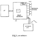
- FIG. 1 relating to art previous ordering crystal display screens liquids includes a DC controller circuit controlled by a ⁇ P microprocessor.
- This DC controller circuit includes a controller C and a charge pump allowing from a value supply voltage normalized, 5 V for example, to generate voltages of higher amplitude control, up to 9 V.
- Control voltages are delivered as rectangular voltages of given amplitude, 1.8 V, and switched between the ground voltage and the different successive levels up to the maximum voltage delivered by the charge pump, 6 levels from 0 to 9 volts per step of 1.8 volts, these rectangular level voltages different allowing in fact to adjust the level of contrast as a function of the address of the LCD segments orders.
- a solution to reduce variations of the contrast applied may consist of using at the output of the value resistance controller circuit which, by increasing the value of the current, reduce the relative variation of contrast.
- the object of the present invention is to remedy the disadvantages and limitations of controller circuits LCD display screens by the implementation of a device for generating an analog control voltage of stable value and low consumption.
- Another object of the present invention is also, thanks to the implementation of the device analog value control voltage generator stable and low consumption, the increase by a factor at least equal to 75 of the standby time embedded or portable computer systems equipped LCD liquid crystal display screens.
- Another object of the present invention is also an elimination of external capacities on the intermediate levels of the divider bridge, which allows, by integration of the latter, a reduction in the number of inputs / outputs and a reduction in the size of the chip.
- Another object of the present invention is also, due to the very low consumption of the whole, the implementation of a charge pump of reduced size, the external capacities of the pump load can be removed, a reduction corresponding to the size of the chip.
- an object of the present invention is to reduced integration costs and, because low consumption, increased autonomy and display accuracy.
- the device generating an analog control voltage of stable value and low consumption, from an analog voltage of determined nominal value, object of the invention is remarkable in that it comprises an input circuit receiving this analog voltage of determined nominal value making it possible to generate an image analog voltage of reduced value in a determined ratio k.
- a control circuit receives this analog image voltage as a set value and an image signal of the analog control voltage, image signal formed by this analog control voltage reduced in the same determined ratio k.
- This control circuit comprises at least one differential amplifier supplied by a first constant voltage of amplitude greater than the maximum value of the analog image voltage and by a second constant voltage of determined amplitude and delivers a first synchronous switching control pulse of the setpoint signal and amplitude lower than the first constant voltage and a second control pulse synchronous switching of the setpoint signal but complemented with respect to the first control pulse.
- a circuit for switching the analog control voltage, supplied by the analog voltage of determined value, is provided, this switch circuit comprising at least a first switching branch formed by an inverter / amplifier, controlled by the first switching control pulse.
- the device generating an analog voltage stable value control with low consumption, object of the invention finds application to the command of circuits based on control signals of the running type stairs, circuits such as LCD display screens by example, especially when these devices are put implemented in the form of integrated circuits in technology CMOS.
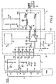
- the external resistances connected in series and denoted r 2 , r 3 , r 4 , r 5 , r 6 are shown , these resistors connected in series connecting the output of the charge pump delivering the voltage Vlcd. constituting the analog voltage of nominal value determined at the output of a pulse modulator device noted PWM, the resistors in series r 2 to r 6 thus delivering voltages V 2 , V 3 , V 4 , V 5 , V 6 , as shown in FIG. 2 and in FIG. 1, in the form of a pulse of given amplitude comprised between the value zero and a maximum value.
- the PWM pulse modulator device makes it possible to adjust the contrast applied to the liquid crystal display via the voltages V 2 to V 6 previously mentioned.
- the device which is the subject of the invention comprises an input circuit 1 receiving the analog voltage Vlcd of given nominal value, as well as of course the voltages V 5 , V 4 , V 3 , V 2 intended to accompany the analog voltage of nominal value in order to obtain the desired contrast at the abovementioned liquid crystal display.
- the input circuit 1 makes it possible to generate an analog image voltage, denoted Vjp, of reduced value in a determined ratio k.
- Vjp analog image voltage
- Vlcd of given nominal value
- V 2 , V 3 , V 4 , V 5 , V 6 is subject to the same reduction in the ratio k given previously cited.
- a set of reduced values is thus obtained, which are denoted Vj 6 , Vj 5 , Vj 4 , Vj 3 , Vj 2 , each corresponding to the voltage values V 6 , V 5 , V 4 , V 3 , V 2 respectively.
- the device which is the subject of the present invention comprises a control circuit 2 receiving the analog image voltage Vjp, that is to say Vj 2 to Vj 6 , this analog image voltage Vjp constituting in fact a set value, denoted V CONS , and an image signal Si of the analog control voltage V SEG0 , this image signal being formed by the aforementioned analog control voltage reduced in the same determined ratio k.
- the control circuit 2 comprises at least one differential amplifier 20, which in fact receives the set value V CONS and the image signal Si previously mentioned.
- the differential amplifier 20 is supplied by a first constant voltage, denoted V 21 , and by a second constant voltage, denoted V 22 , of determined amplitude.
- V 21 a first constant voltage
- V 22 a second constant voltage
- the first constant voltage V 21 is greater than the maximum value of the analog image voltage Si previously mentioned.
- the first constant voltage V 21 is a low voltage which serves as a power supply and which reduces consumption.
- the input levels of the differential amplifier 20 must be lower than that of the first supply voltage V 21 , hence the reduction by k.
- the differential amplifier 20 delivers a first switching control pulse, denoted V OUTPLUSP , this first pulse being synchronous with the reference signal V CONS and of amplitude less than the first constant voltage V 21 .
- the differential amplifier 20 also delivers a second switching control pulse, denoted V OUTMOINSP , synchronous with the reference signal V CONS but supplemented with respect to the first control pulse V OUTMOINSP .
- the device which is the subject of the invention comprises a circuit 3 for switching the analog control voltage V SEG0 .
- This circuit is supplied by the analog voltage of determined nominal value Vlcd and comprises at least a first switching branch, denoted SW 1 , formed by an inverter / amplifier, this first switching branch being controlled by the first switching control pulse V OUTPLUSP and delivering a pulse, denoted V -HI-OUT , of amplified auxiliary switching control, the latter being synchronous with the reference signal V CONS .
- the switching circuit 3 comprises a second switching branch, designated SW 2 , formed by an inverter / amplifier and controlled by the amplified auxiliary switching control pulse V -HI-OUT and by the second control pulse. switching V OUTMOINSP .
- the second switching branch SW 2 thus delivers the analog control voltage V SEG0 switched to the analog voltage of determined nominal value Vlcd.
- Figure 2 there is shown the output of the circuit 3 for switching the analog control voltage, constituting in fact the output of the device generating an analog control voltage object of the invention, connected to a capacity of the order of 170 pF to 200 pF representing the input capacity of the segments of the LCD display to be controlled.
- the input circuit 1 comprises at least one divider bridge Rj, denoted R 2 to R 6 in FIG. 2, only the divider bridges R 6 and R 5 , for reasons of simplification of the drawings, being shown in the above figure.
- Each divider bridge receives the analog voltage of nominal value Vj, that is to say V 6 , V 3 , V 2 , and delivers the analog voltage image of reduced value in the determined ratio k.
- Vj 6 , Vj 5 , Vj 4 , Vj 3 and Vj 2 the analog image voltage of reduced value is designated by Vj 6 , Vj 5 , Vj 4 , Vj 3 and Vj 2 , each of these voltages being in fact delivered by the divider bridge R 6 to R 2 corresponding.
- the input circuit 1 can include, without limitation, an analog gate Pj, in fact a set of elementary gates denoted P 1 to P 6 in FIG. 2, each analog gate Pj having a threshold value corresponding to the value of the analog image voltage of reduced value Vj 2 to Vj 6 , the corresponding analog gate delivering the analog image voltage Vjp of reduced value.
- an analog gate Pj in fact a set of elementary gates denoted P 1 to P 6 in FIG. 2, each analog gate Pj having a threshold value corresponding to the value of the analog image voltage of reduced value Vj 2 to Vj 6 , the corresponding analog gate delivering the analog image voltage Vjp of reduced value.
- control circuit 2 includes a divider bridge, denoted R CONS , this divider bridge being a bridge whose division ratio is equal to the ratio k of the determined value mentioned above.
- the aforementioned divider bridge receives the analog control voltage V SEG0 . and delivers the image signal Si of the above-mentioned analog control voltage.
- the differential amplifier 20 included in the control circuit 2 comprises a first input of a first stable reference voltage V 21 allowing the supply of the aforementioned differential amplifier.
- the first stable reference voltage V 21 is chosen at a first voltage level of determined value.
- the differential amplifier comprises a second input of a second stable reference voltage V 22 , which is chosen at a second voltage level value.
- the stable reference supply voltages V 21 and V 22 can advantageously be delivered by corresponding circuits 21 and 22, which, from a same stable reference voltage V 0 delivered by a "band gap" type circuit in Anglo-Saxon language, can deliver a first stable reference voltage at an intensity of the order of 200 ⁇ A for circuit 21, and a second stable reference voltage at an intensity of a few ⁇ A for the circuit 22.
- the reference voltage V 0 supplying the circuits 21 and 22 can be chosen to be equal to 1.25 V, for example from the aforementioned "band gap" type circuits.
- the differential amplifier 20 supplied under these conditions receives on a positive terminal Vp the image voltage Vjp delivered by the corresponding divider bridge Rj and of course by the corresponding logic gate Pj, and on its negative terminal denoted Vn the image signal Si delivered itself by the divider bridge R CONS previously mentioned in the description.
- the differential amplifier 20 delivers, on the one hand, the first control pulse switching and, secondly, the second pulse of switching control previously mentioned in the description.
- the above-mentioned circuit 3 may advantageously include a first inverter / amplifier forming the first switching branch, denoted SW 1 .
- the first amplifier inverter comprises a PMOS transistor denoted PM 1 and an NMOS transistor denoted NM 1 , these transistors being connected in cascade by their common drain / source point between the analog voltage of nominal value Vlcd and the reference voltage Vref, also designated by ground voltage.
- the gate electrode of the PMOS transistor PM 1 of the first branch receives a bias voltage equal to a fraction of the analog voltage of nominal value and the gate electrode of this transistor receives the first switching control pulse V OUTPLUSP previously mentioned in the description.
- the PMOS transistor PM 1 plays the role of a resistor, while the NMOS transistor NM 1 controlled by the first aforementioned control pulse can then play the role of an inverter switch, the common drain / source point between the aforementioned transistors delivering the amplified auxiliary switching control pulse V -HI-OUT previously mentioned in the description.
- the switching circuit 3 includes the second amplifier inverter forming the second switching branch SW 2 . It includes a PMOS transistor PM 2 and an NMOS transistor NM 2 connected in cascade by their common drain / source point between the analog voltage of determined nominal value Vlcd and the reference voltage Vref.
- the gate electrode of the PMOS transistor PM 2 receives the amplified auxiliary switching control pulse V -HI-OUT , that is to say the voltage delivered by the common drain / source point of the transistors PM 1 and NM 1 of the first branch SW 1 .
- the gate electrode of the NMOS transistor NM 2 of the second branch SW 2 receives the second switching control pulse delivered by the differential amplifier 20.
- the common drain / source point of the PMOS PM 2 transistors and NMOS NM 2 of the second branch SW 2 delivers the analog control voltage V SEG0 of stable value and with low consumption switched to the value of the analog voltage of determined nominal value Vlcd previously mentioned in the description.
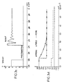
- FIG. 3b the evolution of the first control pulse V OUTPLUSP and of the second control pulse V OUTMOINSP is shown . It can be seen that the aforementioned control pulses are synchronous with the reference signal but substantially complemented, the first control pulse evolving between a low analog value substantially equal to 1 V and a high analog value less than the first constant voltage supplying the differential amplifier 20, this first constant voltage V 21 having been chosen at 2.7 V.
- the high analog voltage of the first control pulse is of the order of 2.3 V.
- the second control pulse evolves between a first high analog value substantially equal to 0.3 V and a second low analog voltage substantially equal to 0 V for the complemented parts with respect to the first control pulse.
- control pulses and in particular the difference between the signals and the respectively low and high analog values of the latter, differences substantially equal to 2.3 V, is then in a way amplified by the first switching branch circuits SW 1 and second switching branch SW 2 constituting the switching circuit 3 under the conditions below.
- the first control pulse V OUTPLUSP causes by switching of the transistor NM 1 of the first switching branch SW 1 the appearance of the amplified auxiliary control pulse V -HI-OUT by transition between the value 6.8 V and 0 V, this auxiliary control pulse being inverted with respect to the first control pulse. While the first control pulse is at the high analog value while the second control pulse is at the low analog value, the PM 2 transistor is then conductive, the junction point between the PMOS PM 2 transistor and NMOS NM 2 of the second switching branch SW 2 then being switched to the aforementioned nominal voltage analog value Vlcd.
- the voltage at test point C changes as shown in FIG. 3a with a time constant determined by the value of the load capacity of the segments of the LCD display.
- the image voltage Si changes accordingly, which makes it possible to reduce the difference at the input of the differential amplitude 20 and thus the switching at equilibrium of the first and second switching control pulses, as shown in FIG. 3b.
- the transistor PM 2 of the second switching branch SW 2 is turned off and the voltage at the test point C is then established at the load value corresponding to the analog voltage of nominal value Vlcd.
- the transient switching phenomena are represented in FIG. 3c following the switching of the PM 2 transistor previously mentioned. The segment is then charged to the nominal voltage value previously mentioned.
- the first switching control pulse V OUTPLUSP then passes in synchronism with the reference signal from a value of 1 V to the value of 0 V, whereas on the contrary the second pulse of the switching control V OUTMOINSP goes from the value 0.3 V to the maximum value 1.8 V. While the analog low level value of the first switching control pulse remains substantially equal to zero during the balancing of the voltages at the input of the differential amplifier 20, the high analog value of the second switching control pulse V OUTMOINSP decreases in a substantially regular manner until the voltages Vp and Vm are balanced at the input of the differential amplifier 20.
- the transistor PM 2 of the second switching branch SW 2 remains blocked, because it passes from a semi-blocked state close to the blocking value V T (7V) to a state blocked. It is the second control pulse V OUTMOINSP as represented in FIG. 3 which goes to 1.8 volts and therefore to a value greater than the blocking value V T (0.7 V) of the NMOS transistor NM 2 of the second switching branch. The transistor NM 2 is then conductive and the discharge of the output, as shown in FIG. 3f, is carried out.
- the initial state is then restored, the transistor NM 2 of the second switching branch SW 2 being blocked and the voltage V SEG0 having reached the new analog nominal voltage value Vlcd.
- the PM 2 transistor is used for charging and the NM 2 transistor for discharging the output.
- Figure 3g shows different transitions successively in discharge, in charge, transition amplitude of 1.8 V, then under load, transition amplitude of 3.6 V, then again in discharge, 5.4 V amplitude transition, k times the signal of instructions.
Landscapes
- Engineering & Computer Science (AREA)
- Chemical & Material Sciences (AREA)
- Crystallography & Structural Chemistry (AREA)
- Physics & Mathematics (AREA)
- Computer Hardware Design (AREA)
- General Physics & Mathematics (AREA)
- Theoretical Computer Science (AREA)
- Control Of Indicators Other Than Cathode Ray Tubes (AREA)
- Liquid Crystal Display Device Control (AREA)
Applications Claiming Priority (2)
| Application Number | Priority Date | Filing Date | Title |
|---|---|---|---|
| FR9914349A FR2801148B1 (fr) | 1999-11-16 | 1999-11-16 | Commande analogique controlee |
| FR9914349 | 1999-11-16 |
Publications (1)
| Publication Number | Publication Date |
|---|---|
| EP1102235A1 true EP1102235A1 (de) | 2001-05-23 |
Family
ID=9552142
Family Applications (1)
| Application Number | Title | Priority Date | Filing Date |
|---|---|---|---|
| EP00403152A Withdrawn EP1102235A1 (de) | 1999-11-16 | 2000-11-13 | Spannungsgenerator für Flüssigkristallanzeige mit Spannungsteiler, Differenzverstärker und Schaltkreis |
Country Status (3)
| Country | Link |
|---|---|
| US (1) | US6346903B1 (de) |
| EP (1) | EP1102235A1 (de) |
| FR (1) | FR2801148B1 (de) |
Cited By (1)
| Publication number | Priority date | Publication date | Assignee | Title |
|---|---|---|---|---|
| CN101334680B (zh) * | 2007-06-29 | 2011-04-20 | 群康科技(深圳)有限公司 | 公共电压产生电路及液晶显示装置 |
Families Citing this family (4)
| Publication number | Priority date | Publication date | Assignee | Title |
|---|---|---|---|---|
| DE60204850T2 (de) * | 2001-02-01 | 2006-05-11 | Koninklijke Philips Electronics N.V. | Programmierbares ladungspumpenbauelement |
| KR100527089B1 (ko) * | 2002-11-04 | 2005-11-09 | 비오이 하이디스 테크놀로지 주식회사 | 액정표시장치의 공통전압 조정회로 |
| CN101140735B (zh) * | 2006-09-04 | 2011-12-28 | 意法半导体研发(上海)有限公司 | 用集成可编程电阻阵列调节vcom电平的方法 |
| EP3461004B1 (de) * | 2017-09-20 | 2021-04-28 | Nxp B.V. | Verstärker und empfänger für drahtloses signal mit diesem verstärker |
Citations (6)
| Publication number | Priority date | Publication date | Assignee | Title |
|---|---|---|---|---|
| GB2010038A (en) * | 1977-12-07 | 1979-06-20 | Tokyo Shibaura Electric Co | Operational amplifier |
| EP0479304A2 (de) * | 1990-10-05 | 1992-04-08 | Kabushiki Kaisha Toshiba | Leistungsquellenapparat zum Steuern eines Flüssigkristallanzeigegeräts |
| EP0570001A2 (de) * | 1992-05-14 | 1993-11-18 | Kabushiki Kaisha Toshiba | Flüssigkristallanzeigegerät |
| US5561442A (en) * | 1993-04-01 | 1996-10-01 | Sharp Kabushiki Kaisha | Method and circuit for driving a display device |
| JPH1174742A (ja) * | 1997-08-27 | 1999-03-16 | Denso Corp | オペアンプ |
| EP0915361A1 (de) * | 1997-04-22 | 1999-05-12 | Matsushita Electric Industrial Co., Ltd. | Treiberschaltung für aktiv-matrix-flüssigkristallanzeige |
Family Cites Families (2)
| Publication number | Priority date | Publication date | Assignee | Title |
|---|---|---|---|---|
| DE4134539A1 (de) * | 1991-10-18 | 1993-04-22 | Gao Ges Automation Org | Aufzeichnungstraeger mit farbigen bildinformationen, insbesondere wert- oder ausweiskarte |
| US5739804A (en) * | 1994-03-16 | 1998-04-14 | Kabushiki Kaisha Toshiba | Display device |
-
1999
- 1999-11-16 FR FR9914349A patent/FR2801148B1/fr not_active Expired - Fee Related
-
2000
- 2000-11-13 US US09/709,654 patent/US6346903B1/en not_active Expired - Lifetime
- 2000-11-13 EP EP00403152A patent/EP1102235A1/de not_active Withdrawn
Patent Citations (6)
| Publication number | Priority date | Publication date | Assignee | Title |
|---|---|---|---|---|
| GB2010038A (en) * | 1977-12-07 | 1979-06-20 | Tokyo Shibaura Electric Co | Operational amplifier |
| EP0479304A2 (de) * | 1990-10-05 | 1992-04-08 | Kabushiki Kaisha Toshiba | Leistungsquellenapparat zum Steuern eines Flüssigkristallanzeigegeräts |
| EP0570001A2 (de) * | 1992-05-14 | 1993-11-18 | Kabushiki Kaisha Toshiba | Flüssigkristallanzeigegerät |
| US5561442A (en) * | 1993-04-01 | 1996-10-01 | Sharp Kabushiki Kaisha | Method and circuit for driving a display device |
| EP0915361A1 (de) * | 1997-04-22 | 1999-05-12 | Matsushita Electric Industrial Co., Ltd. | Treiberschaltung für aktiv-matrix-flüssigkristallanzeige |
| JPH1174742A (ja) * | 1997-08-27 | 1999-03-16 | Denso Corp | オペアンプ |
Cited By (1)
| Publication number | Priority date | Publication date | Assignee | Title |
|---|---|---|---|---|
| CN101334680B (zh) * | 2007-06-29 | 2011-04-20 | 群康科技(深圳)有限公司 | 公共电压产生电路及液晶显示装置 |
Also Published As
| Publication number | Publication date |
|---|---|
| FR2801148B1 (fr) | 2002-01-18 |
| FR2801148A1 (fr) | 2001-05-18 |
| US6346903B1 (en) | 2002-02-12 |
Similar Documents
| Publication | Publication Date | Title |
|---|---|---|
| EP3509219B1 (de) | Kompensierter komparator | |
| FR2793934A1 (fr) | Procede et systeme de pilotage de lignes de donnees et dispositif d'affichage a cristal liquide l'utilisant | |
| EP0838745A1 (de) | Spannungsregler mit automatischer Auswahl der höchsten Versorgungsspannung | |
| FR3032309A1 (fr) | Circuit de regulation de tension adapte aux fortes et faibles puissances | |
| EP1380913B1 (de) | Linearer Spannungsregler | |
| FR2756984A1 (fr) | Alimentation de secours destinee a suppleer provisoirement a une carence d'une source d'alimentation principale | |
| WO1999031650A1 (fr) | Dispositif de commande d'une cellule d'un ecran matriciel | |
| FR3070774A1 (fr) | Procede de compensation de chute de tension sur un cable usb type c, et circuit correspondant | |
| EP1102235A1 (de) | Spannungsgenerator für Flüssigkristallanzeige mit Spannungsteiler, Differenzverstärker und Schaltkreis | |
| EP2337205A1 (de) | Stromzuführung mit Mehrstufen-Partitionierung | |
| FR2702105A1 (fr) | Dispositif de régulation de la tension de mode commun en sortie d'un amplificateur équilibré. | |
| FR2763765A1 (fr) | Commutateur de courant et boucle a phase asservie utilisant ce commutateur | |
| EP1835373B1 (de) | Erzeugung einer Bezugsspannung | |
| EP1697920B1 (de) | Vorrichtung zum anzeigen von bildern auf einer oled aktivmatrix | |
| EP0453040A1 (de) | Leistungsverstärker, insbesondere für Rechtecksignale | |
| EP0554196A1 (de) | Telefonleitungsstrommodulator | |
| FR2805682A1 (fr) | Dispositif de comparaison a tres base consommation | |
| EP1258975B1 (de) | Regelungsschaltung für Hochspannungsgenerator | |
| FR2884371A1 (fr) | Dispositif de decalage de niveau de tension | |
| EP0838746B1 (de) | Spannungsregler | |
| FR2872305A1 (fr) | Procede de controle du fonctionnement d'un regulateur a faible chute de tension et circuit integre correspondant | |
| FR3103581A1 (fr) | Pompe de charge | |
| FR2758021A1 (fr) | Circuit elevateur de tension | |
| FR2777139A1 (fr) | Oscillateur a frequence controlee en courant, a reponse rapide | |
| EP4517473B1 (de) | Spannungsregler |
Legal Events
| Date | Code | Title | Description |
|---|---|---|---|
| PUAI | Public reference made under article 153(3) epc to a published international application that has entered the european phase |
Free format text: ORIGINAL CODE: 0009012 |
|
| AK | Designated contracting states |
Kind code of ref document: A1 Designated state(s): DE GB IT NL |
|
| AX | Request for extension of the european patent |
Free format text: AL;LT;LV;MK;RO;SI |
|
| 17P | Request for examination filed |
Effective date: 20010602 |
|
| AKX | Designation fees paid |
Free format text: DE GB IT NL |
|
| 17Q | First examination report despatched |
Effective date: 20071220 |
|
| STAA | Information on the status of an ep patent application or granted ep patent |
Free format text: STATUS: THE APPLICATION IS DEEMED TO BE WITHDRAWN |
|
| 18D | Application deemed to be withdrawn |
Effective date: 20110601 |