EP1103831A2 - Circuit opto-électronique à puce inversée - Google Patents
Circuit opto-électronique à puce inversée Download PDFInfo
- Publication number
- EP1103831A2 EP1103831A2 EP00122783A EP00122783A EP1103831A2 EP 1103831 A2 EP1103831 A2 EP 1103831A2 EP 00122783 A EP00122783 A EP 00122783A EP 00122783 A EP00122783 A EP 00122783A EP 1103831 A2 EP1103831 A2 EP 1103831A2
- Authority
- EP
- European Patent Office
- Prior art keywords
- chip
- integrated circuit
- substrate
- components
- circuit
- Prior art date
- Legal status (The legal status is an assumption and is not a legal conclusion. Google has not performed a legal analysis and makes no representation as to the accuracy of the status listed.)
- Withdrawn
Links
- 230000005693 optoelectronics Effects 0.000 title claims abstract description 28
- 239000000758 substrate Substances 0.000 claims abstract description 67
- 239000013307 optical fiber Substances 0.000 claims abstract description 6
- 238000004891 communication Methods 0.000 claims abstract description 3
- 238000000034 method Methods 0.000 claims description 17
- 230000005540 biological transmission Effects 0.000 claims description 6
- 239000003990 capacitor Substances 0.000 claims description 5
- 239000000872 buffer Substances 0.000 claims description 3
- 238000005476 soldering Methods 0.000 claims 1
- 230000003287 optical effect Effects 0.000 abstract description 18
- 229910000679 solder Inorganic materials 0.000 abstract description 12
- 238000013461 design Methods 0.000 abstract description 4
- 238000004519 manufacturing process Methods 0.000 description 9
- 230000008901 benefit Effects 0.000 description 5
- 230000008569 process Effects 0.000 description 5
- 238000013459 approach Methods 0.000 description 4
- 230000010354 integration Effects 0.000 description 4
- 239000000463 material Substances 0.000 description 4
- 238000010586 diagram Methods 0.000 description 3
- 230000003993 interaction Effects 0.000 description 3
- 229910052751 metal Inorganic materials 0.000 description 3
- 239000002184 metal Substances 0.000 description 3
- 230000003071 parasitic effect Effects 0.000 description 3
- MDPILPRLPQYEEN-UHFFFAOYSA-N aluminium arsenide Chemical compound [As]#[Al] MDPILPRLPQYEEN-UHFFFAOYSA-N 0.000 description 2
- 238000001465 metallisation Methods 0.000 description 2
- 230000004044 response Effects 0.000 description 2
- 239000004065 semiconductor Substances 0.000 description 2
- 235000012431 wafers Nutrition 0.000 description 2
- 229910001218 Gallium arsenide Inorganic materials 0.000 description 1
- GPXJNWSHGFTCBW-UHFFFAOYSA-N Indium phosphide Chemical compound [In]#P GPXJNWSHGFTCBW-UHFFFAOYSA-N 0.000 description 1
- PNEYBMLMFCGWSK-UHFFFAOYSA-N aluminium oxide Inorganic materials [O-2].[O-2].[O-2].[Al+3].[Al+3] PNEYBMLMFCGWSK-UHFFFAOYSA-N 0.000 description 1
- 230000003321 amplification Effects 0.000 description 1
- 238000006243 chemical reaction Methods 0.000 description 1
- 150000001875 compounds Chemical class 0.000 description 1
- 238000010276 construction Methods 0.000 description 1
- 230000008878 coupling Effects 0.000 description 1
- 238000010168 coupling process Methods 0.000 description 1
- 238000005859 coupling reaction Methods 0.000 description 1
- 238000001514 detection method Methods 0.000 description 1
- 239000000835 fiber Substances 0.000 description 1
- 230000005669 field effect Effects 0.000 description 1
- 239000012212 insulator Substances 0.000 description 1
- 238000003199 nucleic acid amplification method Methods 0.000 description 1
- 238000012545 processing Methods 0.000 description 1
- 239000010453 quartz Substances 0.000 description 1
- 229910052710 silicon Inorganic materials 0.000 description 1
- 239000010703 silicon Substances 0.000 description 1
- VYPSYNLAJGMNEJ-UHFFFAOYSA-N silicon dioxide Inorganic materials O=[Si]=O VYPSYNLAJGMNEJ-UHFFFAOYSA-N 0.000 description 1
- 239000010409 thin film Substances 0.000 description 1
- 230000026683 transduction Effects 0.000 description 1
- 238000010361 transduction Methods 0.000 description 1
Images



Classifications
-
- G—PHYSICS
- G02—OPTICS
- G02B—OPTICAL ELEMENTS, SYSTEMS OR APPARATUS
- G02B6/00—Light guides; Structural details of arrangements comprising light guides and other optical elements, e.g. couplings
- G02B6/24—Coupling light guides
- G02B6/42—Coupling light guides with opto-electronic elements
- G02B6/4201—Packages, e.g. shape, construction, internal or external details
- G02B6/4219—Mechanical fixtures for holding or positioning the elements relative to each other in the couplings; Alignment methods for the elements, e.g. measuring or observing methods especially used therefor
- G02B6/4228—Passive alignment, i.e. without a detection of the degree of coupling or the position of the elements
- G02B6/4232—Passive alignment, i.e. without a detection of the degree of coupling or the position of the elements using the surface tension of fluid solder to align the elements, e.g. solder bump techniques
-
- H—ELECTRICITY
- H10—SEMICONDUCTOR DEVICES; ELECTRIC SOLID-STATE DEVICES NOT OTHERWISE PROVIDED FOR
- H10F—INORGANIC SEMICONDUCTOR DEVICES SENSITIVE TO INFRARED RADIATION, LIGHT, ELECTROMAGNETIC RADIATION OF SHORTER WAVELENGTH OR CORPUSCULAR RADIATION
- H10F39/00—Integrated devices, or assemblies of multiple devices, comprising at least one element covered by group H10F30/00, e.g. radiation detectors comprising photodiode arrays
- H10F39/10—Integrated devices
- H10F39/107—Integrated devices having multiple elements covered by H10F30/00 in a repetitive configuration, e.g. radiation detectors comprising photodiode arrays
-
- G—PHYSICS
- G02—OPTICS
- G02B—OPTICAL ELEMENTS, SYSTEMS OR APPARATUS
- G02B6/00—Light guides; Structural details of arrangements comprising light guides and other optical elements, e.g. couplings
- G02B6/24—Coupling light guides
- G02B6/42—Coupling light guides with opto-electronic elements
- G02B6/4201—Packages, e.g. shape, construction, internal or external details
- G02B6/4219—Mechanical fixtures for holding or positioning the elements relative to each other in the couplings; Alignment methods for the elements, e.g. measuring or observing methods especially used therefor
- G02B6/4228—Passive alignment, i.e. without a detection of the degree of coupling or the position of the elements
- G02B6/423—Passive alignment, i.e. without a detection of the degree of coupling or the position of the elements using guiding surfaces for the alignment
-
- G—PHYSICS
- G02—OPTICS
- G02B—OPTICAL ELEMENTS, SYSTEMS OR APPARATUS
- G02B6/00—Light guides; Structural details of arrangements comprising light guides and other optical elements, e.g. couplings
- G02B6/24—Coupling light guides
- G02B6/42—Coupling light guides with opto-electronic elements
- G02B6/4201—Packages, e.g. shape, construction, internal or external details
- G02B6/4246—Bidirectionally operating package structures
Definitions
- the present invention relates generally to integrated optoelectronic circuit devices and integrated microwave devices and more particularly to a two-part optoelectronic circuit.
- Optoelectronics pertains to the interaction of electronic processes with optical processes. This interaction is typically associated with energy conversion between electrical signals and optical signals.
- Optoelectronic devices such as lasers, photodetectors, optical modulators, and optical switches, are examples of devices within which this interaction takes place.
- the hybrid integration connects discrete devices with electrical interconnects. Many individual devices are mounted separately on a carrier. Interconnections between the devices are typically accomplished through bond wires or metal paths formed on the carrier substrate.
- This approach has high flexibility since the devices are selected and interconnected according to the needs of a given application. However, this approach generally results in large circuit size and high parasitics relative to monolithic circuits. The advantage is that semiconductor materials and fabrication processes can be independently selected to enhance the performance of each device.
- the hybrid approach is well suited for constructing prototypes. Production can be costly if the circuit contains many devices and interconnections. Additionally, the many separate devices must be tested and mounted individually.
- Monolithic integration places all active and passive components on the same substrate. In addition to reducing the overall circuit size, this process reduces parasitic inductances and capacitances because it shortens the length of circuit interconnect structures.
- Monolithic circuits are typically formed with compound semiconductor families, for example, gallium aluminum arsenide (GaAlAs) and indium phosphide (InP), that inherently facilitate the realization of high resistivity substrates which reduce microwave losses and crosstalk in electrical interconnects.
- the monolithic integration approach is particularly suited for high volume applications. Since many circuit chips can be obtained from a single wafer and several wafers can be processed in a given fabrication run, the cost of a fabrication run is shared among the many units produced. However, each integrated circuit is designed for a specific purpose. Therefore, different applications must be served by designing and fabricating entirely new chips. The tooling cost associated with each new application is high and may not be justifiable when small volumes are needed.
- the present invention facilitates an application-specific rf-optoelectronic circuit by combining at least one generic chip, having common building-block components, with a defining substrate, having application-specific circuit parts and patterns.
- the same generic chip can be used in many different applications, and the defining substrate is specific to each application.
- the generic chip contains building block components that perform functions such as, but not limited to, optical detection and generation, optical modulation, electrical switching and latching, and electrical amplification.
- the generic chip can be used in any application due to the fact that paths external to the generic chip connect the building block circuit parts on the generic chip.
- the defining substrate consists of passive electronic and microwave components such as, but not limited to, capacitors, inductors, resistors and transmission line elements. These passive components provide electrical and optical interconnection between selected building block components on the generic chip and define the specific function of the combined chip/substrate circuit.
- the components on the defining substrate can determine the gain, frequency response, input/output impedances, logic function, and optical interference according to the needs of a specific application.
- the defining substrate determines the overall function, so the same generic chip can be used in combination with different versions of defining substrates to perform a variety of application-specific functions.
- a further object of the present invention to use at least one generic chip in combination with a defining substrate, wherein the defining substrate determines the overall function of the circuit. Still a further object of the present invention is to maintain inexpensive and relatively fast fabrication of the application specific defining substrate.
- the circuit 10 has two main segments.
- One segment is a generic chip 12 that contains building block circuit parts which will be described in greater detail hereinafter.
- the second segment is a defining substrate 14 that contains application-specific circuit sections.
- the two segments 12 and 14 are connected together electrically and physically, preferably by means of solder bumps 16, which have small, controllable, and well-characterized parasitics.
- the building block circuit parts 18 of the generic device are preferably active devices such as photodetectors, optoelectronic modulators, or light emitters.
- the building block circuit parts 18 can also be active devices such as amplifier stages, rf switches, logical gates and latches.
- Figure 1 there is shown, by way of example, a photodetector 20, a modulator 22, an input amplifier stage 24 and an output buffer 26.
- the various building block circuit parts 18 are electrically separate from each other and are preferably interconnected by a path that is external to the generic chip 12.
- the second segment of the present invention 10 is the defining substrate 14 that has application-specific circuit sections 28 that are preferably passive components.
- the circuit sections 28 may be passive microwave components such as transmission lines, resonators, capacitors, inductors, resistors, and tuning stubs.
- the circuit sections may also be passive optical components such as waveguides, reflectors, and grooves 30 for holding optical fibers 32.
- the generic chip 12 contains separate building block circuit parts that are dispersed throughout the chip 12 and arranged in a manner appropriate for their combination to form a complete optoelectronic circuit when combined with the defining substrate (not shown).
- FIG. 2 shows one of the numerous possible layouts for the generic chip 12 of the present invention.
- the chip 12 is arranged as an array of individual cells 34.
- one row of cells 34 contains an alternating sequence of photodetectors 20 and modulators 22 for surface-normal optical coupling.
- Each device has cathode connection points, anode connection points, and ground connection points (not shown).
- Another row of cells contains transimpedance amplifier blocks 40 and driver blocks 42.
- the feedback resistance of the amplifier 40 and the current capability or output impedance of the driver 42 are adjusted by means of external connection points, 41 and 43 respectively, on the defining substrate, thereby allowing the generic chip 12 to remain as generic as possible.
- Another row of cells 32 contains a buffer stage 44 and two PIN diode switches 46, 48, all having external connection points 50.
- Each external connection point 50 is shown as a solder-bump compatible pad.
- the pattern of cells 34 like the one described above, can be repeated many times. Also, other devices, such as waveguide-coupled optoelectronic devices, and other circuit blocks can be included on the generic chip 12 although not shown in the present example.
- the generic chip 12 can be fabricated by known methods for monolithically integrating optoelectronic devices such as photodetectors, modulators or lasers with electronic devices such as bipolar transistors and field-effect transistors. Another method for fabricating the generic chip 12 is disclosed in U.S. Patent Application Serial No. (PD970599) which is incorporated herein by reference. U.S. Patent Application Serial No. (PD970599) describes a method for fabricating a monolithic optoelectronic transmitter in which the optoelectronic device and a high-performance electronic device are formed from the same epitaxial layers.
- the application-specific defining substrate 14 is described with reference to Figures 3a, 3b, 4a and 4b.
- the substrate 14 is preferably formed from a material that is compatible with the construction of low-loss, high performance passive components. If the circuit carries high-frequency signals, representative substrate materials include alumina, semi-insulating GaAs, high-resistivity silicon and quartz. Passive components are built on the substrate material using conventional, known integrated circuit processing techniques. Representative passive components are transmission lines, (i.e. coplanar waveguides), capacitors, (with, for example, a metal-insulator-metal structure), inductors, (such as spirals), and resistors (made from a thin film of controlled resistivity).
- transmission lines i.e. coplanar waveguides
- capacitors with, for example, a metal-insulator-metal structure
- inductors such as spirals
- resistors made from a thin film of controlled resistivity
- the pattern of circuit components and external connection points on the defining substrate 14 mate with the overall pattern of building blocks on the generic chip 12. Therefore, the layout of the circuit portions on the defining substrate 14 is in three dimensions.
- Figure 3a is a schematic layout of a 2-to-1 switchable optoelectronic receiver 52.
- the receiver 52 accepts rf modulated optical signals 54 at optical inputs to two photodetectors 56 and 58.
- the optical signals 54 are amplified by amplifiers 60 and 62 and sent through PIN switches 64 and 66. Depending on the control voltages to those switches, either or both of the amplified photocurrent signals are sent to an electrical output 67.
- the photodetectors 56, 58, amplifiers 60, 62 and switches 64, 66 are building block components on the generic chip 12, shown in phantom in Figure 3b.
- the passive components, load resistors, R1, R2, and R3, feedback resistors RF1 and RF2, capacitors C1, C2, C3 and C4, inductors I1 and I2, and output 67 are circuit components on the defining substrate 14.
- the three dimensional paths between the circuit components on the defining substrate and the building blocks on the generic chip are defined on the defining substrate 14.
- the electrical paths and passive components define the characteristics for the specific building blocks on the generic chip, creating an application-specific integrated optoelectronic circuit.
- Figure 3b shows the physical layout of the defining substrate for the optoelectronic receiver 52 as it is aligned with the generic chip.
- the labels used to describe the components in Figure 3a are likewise used to describe the components in Figure 3b to show the correlation between the schematic and the defining substrate pattern.
- the generic chip 12 is shown in phantom.
- the paths defined by the substrate 14 are external to the generic chip.
- Figure 4a is a schematic diagram of an optoelectronic repeater.
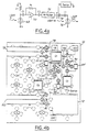
- Figure 4b shows the physical layout of the defining substrate for the repeater as it is assembled with the generic chip (shown in phantom in Figure 4b).
- the defining substrate contacts an input photodetector 68 on the generic chip 12 to a series connection of a transimpedance amplifier 70, also on the generic chip 12.
- the amplifier 70 is connected to an rf filter 72 on the defining substrate 14, and a driver 74 on the generic chip 12.
- An external resistor, R F on the defining substrate sets the gain of the amplifier 70.
- the driver 74 modulates an optoelectronic modulator 76 and has its output impedance set by an external component Z MATCH to match the impedance of the modulator 76.
- Both the optical input and output are coupled to the appropriate devices of the generic chip through optical fibers (not shown).
- the defining substrate has grooves 78, 80, preferably V-shaped, with beam-deflecting mirrors 79, 81, at their ends.
- the grooves 78, 80 are for holding and aligning the fibers (not shown).
- This example illustrates that not only electrical paths, but also optical paths can be defined by the substrate. It should be noted that in both examples, the defining substrates are mated with the exact same generic chip, illustrating the flexibility of the present invention.
- the defining substrate can be fabricated utilizing a method described in U.S. Patent No. 5,611,008 which is incorporated herein by reference.
- a low-loss substrate is provided having a dielectric layer over at least a portion of the substrate.
- Microwave transmission members and passive microwave components are fabricated directly on the dielectric layer.
- the interconnections between the generic chip and the defining substrate essentially define the circuit. Performance characteristics that are defined by the combination of the generic chip and the defining substrate are gain, frequency response, logic function, input/output transduction type, and input/output impedance. It is important that the electrical characteristics of the interconnects are accurately characterized and repeatable from one assembly to the next. Preferably, the interconnects are accomplished through a flip-chip assembly with solder or metal bump interconnections. These assembly methods are common practices and will not be discussed in detail herein.
- Figure 5 illustrates a cross-section of a typical solder-bumped connection.
- the defining substrate 14 has an insulator layer 82, a metalization layer 84, a solder resistant layer 86 (also known as a dam), and solder bump pads 88.
- the generic chip has a metalization layer 84, a solder dam 86 and solder bump pads 88.
- a solder bump 90 contacts the solder bump pads 88 on both the defining substrate 14 and the generic chip 12.
- the solder bump 90 is formed as part of the procedure for making the defining substrate 14.
- the assembly of the combined circuit then consists simply of aligning and placing the generic chip 12 over the substrate 14.
- the chip 12 and substrate 14 are momentarily heated to reflow the solder, thereby forming the connections. This is an extremely fast assembly process and produces a high yield.
- the present invention relates to an application-specific rf optoelectronic integrated circuit having a generic chip member and a defining substrate in communication with at least one generic chip member.
- the generic chip member contains passive building block components that are independent from each other and being connected by paths external to the generic chip member.
- the external connection paths are defined by a defining substrate member having passive components for providing optical and electrical interconnection between selected building block components on the generic chip member to define the specific function of the integrated circuit. It is possible to use the same design of the generic chip for several applications merely by altering the interconnect paths on a defining substrate.
Landscapes
- Physics & Mathematics (AREA)
- General Physics & Mathematics (AREA)
- Optics & Photonics (AREA)
- Optical Couplings Of Light Guides (AREA)
- Optical Communication System (AREA)
- Solid State Image Pick-Up Elements (AREA)
- Design And Manufacture Of Integrated Circuits (AREA)
- Semiconductor Lasers (AREA)
Applications Claiming Priority (2)
| Application Number | Priority Date | Filing Date | Title |
|---|---|---|---|
| US430851 | 1999-11-01 | ||
| US09/430,851 US6285043B1 (en) | 1999-11-01 | 1999-11-01 | Application-specific optoelectronic integrated circuit |
Publications (2)
| Publication Number | Publication Date |
|---|---|
| EP1103831A2 true EP1103831A2 (fr) | 2001-05-30 |
| EP1103831A3 EP1103831A3 (fr) | 2004-02-04 |
Family
ID=23709336
Family Applications (1)
| Application Number | Title | Priority Date | Filing Date |
|---|---|---|---|
| EP00122783A Withdrawn EP1103831A3 (fr) | 1999-11-01 | 2000-10-19 | Circuit opto-électronique à puce inversée |
Country Status (3)
| Country | Link |
|---|---|
| US (2) | US6285043B1 (fr) |
| EP (1) | EP1103831A3 (fr) |
| JP (1) | JP3429270B2 (fr) |
Cited By (2)
| Publication number | Priority date | Publication date | Assignee | Title |
|---|---|---|---|---|
| WO2003065091A3 (fr) * | 2002-01-29 | 2003-11-06 | Qinetiq Ltd | Procede de fabrication de circuit optique et dispositif associe |
| DE10146865B4 (de) * | 2001-09-22 | 2005-04-21 | Mergeoptics Gmbh | Anordnung für ein System zur Datenübertragung |
Families Citing this family (25)
| Publication number | Priority date | Publication date | Assignee | Title |
|---|---|---|---|---|
| DE19855828A1 (de) * | 1998-12-03 | 2000-06-08 | Heidenhain Gmbh Dr Johannes | Dreidimensionales Meßmodul |
| JP3230506B2 (ja) * | 1998-12-28 | 2001-11-19 | 日本電気株式会社 | 受光モジュール |
| US6421473B1 (en) * | 2000-09-28 | 2002-07-16 | Intel Corporation | Method and apparatus for switching an optical beam in an integrated circuit die |
| US6434289B1 (en) | 2000-09-28 | 2002-08-13 | Intel Corporation | Method and apparatus for confining an optical beam in an optical switch |
| US6449405B1 (en) | 2000-09-28 | 2002-09-10 | Intel Corporation | Method and apparatus for switching a plurality of optical beams in an optical switch |
| US6738538B2 (en) * | 2000-10-25 | 2004-05-18 | Patrick R. Antaki | Method to construct optical infrastructure on a wafer |
| US6883977B2 (en) * | 2000-12-14 | 2005-04-26 | Shipley Company, L.L.C. | Optical device package for flip-chip mounting |
| US6781727B2 (en) * | 2000-12-18 | 2004-08-24 | Infineon Technologies Ag | Configuration for operating an optical transmission or reception module at high data rates of up to 10 Gbit/s |
| US6600864B2 (en) * | 2000-12-20 | 2003-07-29 | Intel Corporation | Method and apparatus for switching an optical beam using an optical rib waveguide |
| US6850144B1 (en) | 2001-03-30 | 2005-02-01 | Intel Corporation | Coil for use on a substrate |
| US7031561B2 (en) * | 2001-06-22 | 2006-04-18 | Massachusetts Institute Of Technology | Monolithic integration of micro-optics circuits and RF circuits |
| US7078671B1 (en) * | 2001-08-06 | 2006-07-18 | Shipley Company, L.L.C. | Silicon optical microbench devices and wafer-level testing thereof |
| JP4102043B2 (ja) | 2001-09-20 | 2008-06-18 | 株式会社東芝 | 光通信用モジュール |
| US6936495B1 (en) | 2002-01-09 | 2005-08-30 | Bridge Semiconductor Corporation | Method of making an optoelectronic semiconductor package device |
| US6891276B1 (en) | 2002-01-09 | 2005-05-10 | Bridge Semiconductor Corporation | Semiconductor package device |
| JP2003294964A (ja) * | 2002-04-03 | 2003-10-15 | Sumitomo Electric Ind Ltd | 光通信モジュール |
| US6798964B2 (en) * | 2002-05-01 | 2004-09-28 | Intel Corporation | Method and apparatus for modulating an optical beam in an optical device |
| US7058247B2 (en) * | 2003-12-17 | 2006-06-06 | International Business Machines Corporation | Silicon carrier for optical interconnect modules |
| US7206471B2 (en) * | 2004-12-23 | 2007-04-17 | Lucent Technologies Inc. | Integrated circuit having an optical core |
| US7917042B2 (en) * | 2007-06-29 | 2011-03-29 | Alcatel-Lucent Usa Inc. | High speed optoelectronic receiver |
| FR2979998B1 (fr) | 2011-09-13 | 2013-10-04 | Commissariat Energie Atomique | Dispositif optoelectronique assurant la connexion electrique et optique d'un module optique |
| US20160274318A1 (en) | 2012-03-05 | 2016-09-22 | Nanoprecision Products, Inc. | Optical bench subassembly having integrated photonic device |
| CN106842440A (zh) * | 2012-03-05 | 2017-06-13 | 纳米精密产品股份有限公司 | 用于耦合光纤输入/输出的具有结构化反射表面的耦合装置 |
| US10895683B1 (en) * | 2019-10-14 | 2021-01-19 | Renesas Electronics Corporation | Semiconductor device |
| US12607812B2 (en) * | 2020-03-06 | 2026-04-21 | Sicily Merger Sub II, Inc. | Switch assembly |
Family Cites Families (9)
| Publication number | Priority date | Publication date | Assignee | Title |
|---|---|---|---|---|
| JP3250496B2 (ja) * | 1997-09-19 | 2002-01-28 | 日本電気株式会社 | 光素子実装基板 |
| US4904036A (en) * | 1988-03-03 | 1990-02-27 | American Telephone And Telegraph Company, At&T Bell Laboratories | Subassemblies for optoelectronic hybrid integrated circuits |
| US5138436A (en) * | 1990-11-16 | 1992-08-11 | Ball Corporation | Interconnect package having means for waveguide transmission of rf signals |
| US5237434A (en) * | 1991-11-05 | 1993-08-17 | Mcnc | Microelectronic module having optical and electrical interconnects |
| US5416872A (en) * | 1993-07-06 | 1995-05-16 | At&T Corp. | Arrangement for interconnecting an optical fiber an optoelectronic component |
| US5500910A (en) * | 1994-06-30 | 1996-03-19 | The Whitaker Corporation | Passively aligned holographic WDM |
| US5611008A (en) * | 1996-01-26 | 1997-03-11 | Hughes Aircraft Company | Substrate system for optoelectronic/microwave circuits |
| FI962816A7 (fi) * | 1996-07-11 | 1998-01-12 | Nokia Corp | Mikropiirimodulien kotelorakenne |
| KR100211985B1 (ko) * | 1996-12-11 | 1999-08-02 | 이계철 | 하이브리드 광집적회로용 마이크로 거울, 그의 제조방법, 마이크로 거울-광검출기 어셈블리 및 광수신용 하이브리드 광집적회로 어셈블리 |
-
1999
- 1999-11-01 US US09/430,851 patent/US6285043B1/en not_active Expired - Fee Related
-
2000
- 2000-10-19 EP EP00122783A patent/EP1103831A3/fr not_active Withdrawn
- 2000-11-01 JP JP2000334515A patent/JP3429270B2/ja not_active Expired - Fee Related
-
2001
- 2001-05-25 US US09/865,959 patent/US6495382B2/en not_active Expired - Fee Related
Cited By (3)
| Publication number | Priority date | Publication date | Assignee | Title |
|---|---|---|---|---|
| DE10146865B4 (de) * | 2001-09-22 | 2005-04-21 | Mergeoptics Gmbh | Anordnung für ein System zur Datenübertragung |
| US7428351B2 (en) | 2002-01-28 | 2008-09-23 | Qinetiq Limited | Optical circuit fabrication method and device |
| WO2003065091A3 (fr) * | 2002-01-29 | 2003-11-06 | Qinetiq Ltd | Procede de fabrication de circuit optique et dispositif associe |
Also Published As
| Publication number | Publication date |
|---|---|
| US6285043B1 (en) | 2001-09-04 |
| JP3429270B2 (ja) | 2003-07-22 |
| JP2001189445A (ja) | 2001-07-10 |
| EP1103831A3 (fr) | 2004-02-04 |
| US6495382B2 (en) | 2002-12-17 |
| US20010038100A1 (en) | 2001-11-08 |
Similar Documents
| Publication | Publication Date | Title |
|---|---|---|
| US6285043B1 (en) | Application-specific optoelectronic integrated circuit | |
| US5611008A (en) | Substrate system for optoelectronic/microwave circuits | |
| US6583445B1 (en) | Integrated electronic-optoelectronic devices and method of making the same | |
| US7479401B2 (en) | Front side illuminated photodiode with backside bump | |
| US8265432B2 (en) | Optical transceiver module with optical windows | |
| US20170261708A1 (en) | Compact optical transceiver by hybrid multichip integration | |
| US11177219B1 (en) | Photonic integrated circuit with integrated optical transceiver front-end circuitry for photonic devices and methods of fabricating the same | |
| CN107608040A (zh) | 用于通信的方法和系统 | |
| JPH11231173A (ja) | 高速動作可能な光デバイス | |
| US12562547B2 (en) | Integration method for modularized silicon-based heterogeneous photoelectric integrated architecture | |
| US6912333B2 (en) | Optical interconnection apparatus and interconnection module | |
| US8532449B2 (en) | Wafer integrated optical sub-modules | |
| US10326423B1 (en) | Impedance matching circuits for photonic devices | |
| US12341315B2 (en) | Optical semiconductor chip | |
| Nakahara et al. | Hybrid integration of smart pixels by using polyimide bonding: demonstration of a GaAs pin photodiode/CMOS receiver | |
| Jokerst et al. | Communication through stacked silicon circuitry using integrated thin film InP-based emitters and detectors | |
| CN113994470B (zh) | 共同封装的光学器件和收发器 | |
| US20240219630A1 (en) | Chip package and manufacturing method thereof | |
| US12104950B2 (en) | Optical receiver | |
| Maricot et al. | Monolithic integration of optoelectronic devices with reactive matching networks for microwave applications | |
| CN115440760B (zh) | 半导体结构及其制作方法 | |
| Nordquist et al. | Heterogeneous Integration of Silicon CMOS Electronics and Compound Semiconductor Electronics for Miniature RF Photonic Transceivers | |
| Ohyama et al. | Hybrid integrated differential photoreceiver comprising dual-PD and high-speed GaAs amplifier IC assembled on planar lightwave circuit platform | |
| Ohyama et al. | A differential photoreceiver hybrid integrating a dual-PD and a high-speed GaAs amplifier IC on a planar lightwave circuit platform | |
| Nordquist et al. | Heterogeneous Integration of Silicon Electronics and Compound Semiconductor Optoelectronics for Miniature RF Photonic Transceivers. |
Legal Events
| Date | Code | Title | Description |
|---|---|---|---|
| PUAI | Public reference made under article 153(3) epc to a published international application that has entered the european phase |
Free format text: ORIGINAL CODE: 0009012 |
|
| AK | Designated contracting states |
Kind code of ref document: A2 Designated state(s): AT BE CH CY DE DK ES FI FR GB GR IE IT LI LU MC NL PT SE |
|
| AX | Request for extension of the european patent |
Free format text: AL;LT;LV;MK;RO;SI |
|
| PUAL | Search report despatched |
Free format text: ORIGINAL CODE: 0009013 |
|
| AK | Designated contracting states |
Kind code of ref document: A3 Designated state(s): AT BE CH CY DE DK ES FI FR GB GR IE IT LI LU MC NL PT SE |
|
| AX | Request for extension of the european patent |
Extension state: AL LT LV MK RO SI |
|
| RIC1 | Information provided on ipc code assigned before grant |
Ipc: 7H 01L 25/16 B Ipc: 7G 02B 6/42 A |
|
| 17P | Request for examination filed |
Effective date: 20040702 |
|
| 17Q | First examination report despatched |
Effective date: 20040806 |
|
| AKX | Designation fees paid |
Designated state(s): DE FR GB IT |
|
| STAA | Information on the status of an ep patent application or granted ep patent |
Free format text: STATUS: THE APPLICATION IS DEEMED TO BE WITHDRAWN |
|
| 18D | Application deemed to be withdrawn |
Effective date: 20041217 |