EP1103885B1 - Ecran tactile transparent et affichage a cristaux liquides avec ecran tactile transparent - Google Patents
Ecran tactile transparent et affichage a cristaux liquides avec ecran tactile transparentInfo
- Publication number
- EP1103885B1 EP1103885B1 EP99922626A EP99922626A EP1103885B1 EP 1103885 B1 EP1103885 B1 EP 1103885B1 EP 99922626 A EP99922626 A EP 99922626A EP 99922626 A EP99922626 A EP 99922626A EP 1103885 B1 EP1103885 B1 EP 1103885B1
- Authority
- EP
- European Patent Office
- Prior art keywords
- retardation
- film
- touch panel
- retardation film
- liquid crystal
- Prior art date
- Legal status (The legal status is an assumption and is not a legal conclusion. Google has not performed a legal analysis and makes no representation as to the accuracy of the status listed.)
- Expired - Lifetime
Links
Images

Classifications
-
- G—PHYSICS
- G06—COMPUTING OR CALCULATING; COUNTING
- G06F—ELECTRIC DIGITAL DATA PROCESSING
- G06F3/00—Input arrangements for transferring data to be processed into a form capable of being handled by the computer; Output arrangements for transferring data from processing unit to output unit, e.g. interface arrangements
- G06F3/01—Input arrangements or combined input and output arrangements for interaction between user and computer
- G06F3/03—Arrangements for converting the position or the displacement of a member into a coded form
- G06F3/041—Digitisers, e.g. for touch screens or touch pads, characterised by the transducing means
- G06F3/045—Digitisers, e.g. for touch screens or touch pads, characterised by the transducing means using resistive elements, e.g. a single continuous surface or two parallel surfaces put in contact
-
- G—PHYSICS
- G02—OPTICS
- G02F—OPTICAL DEVICES OR ARRANGEMENTS FOR THE CONTROL OF LIGHT BY MODIFICATION OF THE OPTICAL PROPERTIES OF THE MEDIA OF THE ELEMENTS INVOLVED THEREIN; NON-LINEAR OPTICS; FREQUENCY-CHANGING OF LIGHT; OPTICAL LOGIC ELEMENTS; OPTICAL ANALOGUE/DIGITAL CONVERTERS
- G02F1/00—Devices or arrangements for the control of the intensity, colour, phase, polarisation or direction of light arriving from an independent light source, e.g. switching, gating or modulating; Non-linear optics
- G02F1/01—Devices or arrangements for the control of the intensity, colour, phase, polarisation or direction of light arriving from an independent light source, e.g. switching, gating or modulating; Non-linear optics for the control of the intensity, phase, polarisation or colour
- G02F1/13—Devices or arrangements for the control of the intensity, colour, phase, polarisation or direction of light arriving from an independent light source, e.g. switching, gating or modulating; Non-linear optics for the control of the intensity, phase, polarisation or colour based on liquid crystals, e.g. single liquid crystal display cells
- G02F1/133—Constructional arrangements; Operation of liquid crystal cells; Circuit arrangements
- G02F1/1333—Constructional arrangements; Manufacturing methods
- G02F1/13338—Input devices, e.g. touch panels
-
- G—PHYSICS
- G02—OPTICS
- G02F—OPTICAL DEVICES OR ARRANGEMENTS FOR THE CONTROL OF LIGHT BY MODIFICATION OF THE OPTICAL PROPERTIES OF THE MEDIA OF THE ELEMENTS INVOLVED THEREIN; NON-LINEAR OPTICS; FREQUENCY-CHANGING OF LIGHT; OPTICAL LOGIC ELEMENTS; OPTICAL ANALOGUE/DIGITAL CONVERTERS
- G02F1/00—Devices or arrangements for the control of the intensity, colour, phase, polarisation or direction of light arriving from an independent light source, e.g. switching, gating or modulating; Non-linear optics
- G02F1/01—Devices or arrangements for the control of the intensity, colour, phase, polarisation or direction of light arriving from an independent light source, e.g. switching, gating or modulating; Non-linear optics for the control of the intensity, phase, polarisation or colour
- G02F1/13—Devices or arrangements for the control of the intensity, colour, phase, polarisation or direction of light arriving from an independent light source, e.g. switching, gating or modulating; Non-linear optics for the control of the intensity, phase, polarisation or colour based on liquid crystals, e.g. single liquid crystal display cells
- G02F1/133—Constructional arrangements; Operation of liquid crystal cells; Circuit arrangements
- G02F1/1333—Constructional arrangements; Manufacturing methods
- G02F1/1335—Structural association of cells with optical devices, e.g. polarisers or reflectors
- G02F1/13363—Birefringent elements, e.g. for optical compensation
- G02F1/133634—Birefringent elements, e.g. for optical compensation the refractive index Nz perpendicular to the element surface being different from in-plane refractive indices Nx and Ny, e.g. biaxial or with normal optical axis
Definitions
- the present invention relates to a transparent touch panel capable of preventing the visual recognizing capability by the reflection of the external light from being lowered when the transparent touch panel is mounted to a liquid crystal cell, and to a liquid crystal display device equipped with the transparent touch panel.
- liquid crystal display elements attract attentions as an image display element.
- the liquid crystal display element is expected to be applied to, for example, a portable data assist notebook, an information terminal, a viewing finder for a video camera and a monitor for a car navigation system.
- desired is an input system in which a transparent touch panel is disposed on a display element for performing the input operation while observing the display screen.
- a touch panel of a resistance film type In the conventional touch panel of a resistance film type, a touch panel prepared by using polyethylene terephthalate (PET) film having a transparent conductive film formed thereon and a glass plate having a transparent conductive film formed thereon is superposed on a liquid crystal display element.
- PET polyethylene terephthalate
- JP-A-10-48625 proposes a liquid crystal display device. It is proposed that a touch panel is arranged between a polarizing plate on the display side and a liquid crystal cell, said liquid crystal cell having a liquid crystal material sealed between transparent electrode substrates. Also, a retardation corresponding to 1/4 wavelength of the visible light is imparted to the transparent conductive substrate included in the touch panel. Alternatively, a retardation film is bonded to the transparent conductive substrate so as to prevent the internally reflected light produced by incorporation of the touch panel.
- the PET film used in the past as the touch panel is a crystalline plastic film and, thus, is partially crystallized within the film. As a result, the molecules are nonuniformly oriented, leading to a large unevenness in the retardation. It follows that the PET film cannot be used for the purpose described above. Therefore, it is studied to use a film made of an amorphous plastic material such as polycarbonate, polyarylate, polysulfone, polyether sulfone or a modified polyolefin having a norbornene skeleton.
- an amorphous plastic material such as polycarbonate, polyarylate, polysulfone, polyether sulfone or a modified polyolefin having a norbornene skeleton.
- the touch panel using any of these films permits achieving a desired improvement in the characteristics when viewed in a direction perpendicular to the display surface.
- the contrast is improved and the reflected light is suppressed, compared with the case where the touch panel is combined above the liquid crystal display device, so as to provide a display screen that can be observed very easily.
- the graduation is inverted compared with the displayed image of the liquid crystal display device before integration of the touch panel.
- the monochromatic display is inverted or the color balance of the color display is collapsed so as to bring about practical problems such as deterioration in the quality of the displayed image and the poor viewing angle characteristics of the displayed image.
- EP-A-0 740 181 discloses the use of a retardation film made of amorpous plastic material.
- amorphous transparent plastic materials can be used in the present invention as a plastic material forming a transparent film made of an amorphous plastic material.
- Preferred materials include, for example, bisphenols having an alkylidene group such as bisphenol A as a bisphenol component as well as polycarbonate series plastic materials, polyester carbonate series plastic materials and polyarylate series plastic materials each having bisphenol having a substituted or unsubstituted cycloalkylidene group. It is also possible to use preferably polysulfone, polyether sulfone and norbornene series resins disclosed in JP-A-07-287122.
- the glass transition temperature of these plastic materials is generally desirable for the glass transition temperature of these plastic materials to be not lower than 80°C, preferably to be not lower than 120°C, more preferably to be not lower than 140°C, and most preferably to be not lower than 160°C.
- the film used in the present invention can be prepared by the known film forming methods such as a melt extruding method and a solvent casting method. It is desirable to employ the solvent casting method because it is possible to obtain a film having a smooth surface and small in unevenness in the thickness and in the retardation. In the case of employing the solvent casting method, it is possible to obtain a film having a surface roughness (Ra value) not larger than 100 nm and an unevenness in thickness which is not larger than 5% of the average film thickness.
- Ra value surface roughness
- nz represents the refractive index in a direction perpendicular to nx, which is the maximum refractive index within the film plane
- nz represents the refractive index in the thickness direction of the film.
- the dependence of the displayed image quality on the viewing angle is derived from the fact that the retardation of the film represented by the product between the birefringence (nx - ny) and the thickness d of the film is changed depending on the viewing angle.
- the dependence on the viewing angle can be diminished by meeting the relationship nz > ny in at least one retardation film.
- nx, ny and nz differs depending on the relative arrangement between the retardation film and the touch panel of the liquid crystal cell, making it necessary to determine appropriately by experience the preferred relationship.
- Nz which is represented by (nx - nz)/(nx - ny), .to fall within a range of between 0.9 and 0.1, preferably within a range of between 0.8 and 0.2, and more preferably within a range of between 0.7 and 0.3.
- nx, ny and nz By selecting the values of nx, ny and nz to fall within the range noted above, it is possible to permit the ratio of the retardation Rx(40) or Ry(40) measured in a direction inclined by 40° in a direction of nx or ny to the retardation (R(0)) measured in the direction perpendicular to the film surface, i.e., Rx(40)/R(0) or Ry(40)/R(0), to fall within a range of between 1.08 and 0.90, preferably between 1.05 and 0.95, and 1.03 and 0.96.
- the retardation R(0) is desirable for the retardation R(0) to be 1/4 wavelength relative to the wavelength of the visible light.
- the retardation R(0) falls within a range of between 90 nm and 200 nm, preferably not shorter than 110 nm and not longer than 160 nm. In this case, it is desirable for R(0) to be 1/4 wavelength for each wavelength of the visible light.
- the retardation film is desirable for the retardation film to be formed of an olefinic plastic material such as a norbornene series resin.
- the preferred relationship among nx, ny and nz of one retardation film having a relationship nz > ny differs depending on the optical characteristics of said one retardation film and the other retardation film and the relative arrangement between the liquid crystal cell and the touch panel, making it necessary to determine appropriately by experience the preferred relationship among nx, ny and nz of one retardation film having a relationship nz > ny.
- said one retardation film is formed of a retardation film prepared by uniaxially stretching a plastic material having positive birefringence properties such as polycarbonate, i.e., where one retardation film has the relationship nz > ny, with the other retardation film having the relationship nz ⁇ ny, it is desirable to select the values of nx, ny and nz to permit the Nz value represented by (nx - nz)/(nx - ny) to fall within a range of between -0.9 and 0.8, preferably between -0.7 and 0.4, and more preferably between -0.5 and 0.3.
- each of the two retardation films meets the relationship nz > ny, it is desirable for the Nz value to fall within a range of between 0.9 and 0.1, preferably between 0.8 and 0.2, and more preferably between 0.7 and 0.3.
- the resultant retardation value is zero.
- the retardation value is measured in a direction inclined from the direction perpendicular to the display surface, the retardation value is greatly increased to reach 30 nm or more in the case of using the conventional retardation film, giving rise to inconveniences in the displayed image such as inversion of the color tone and collapse of the color balance.
- a retardation film meeting the relationship nz > ny as at least one of the retardation films it is possible to suppress markedly the increase in the resultant retardation value by selecting an appropriate value.
- the particular retardation film can be manufactured by the known method by orienting the molecules in a predetermined direction.
- the retardation film used in the present invention can be easily obtained by stretching a film made of a material having negative birefringence properties such as polystyrene, as disclosed in JP-A-2-256023.
- the first retardation film is used integral with the polarizing plate.
- strain under stress is applied to the film constituting the touch film because of deformation of the polarizing plate under the environment of the use.
- the birefringence of the film is changed by the strain under stress so as to be deviated from a preferred range.
- an unevenness in the retardation is generated within the plane so as to markedly degrade the displayed image quality.
- the material in which the birefringence tends to be developed to some extent is adapted for the processing because the molecules are easily oriented by stress.
- a stretched film made of a plastic material such as polycarbonate, polyarylate, polysulfone or polyether sulfone or a known amorphous plastic material such as a modified polyolefin, or a norbornene series plastic material can be used as a preferred retardation film used in the present invention.
- a plastic material such as polycarbonate, polyarylate, polysulfone or polyether sulfone or a known amorphous plastic material such as a modified polyolefin, or a norbornene series plastic material
- particularly preferred plastic materials are polyarylate, polycarbonate and polyester carbonate having a bisphenol component having substituted or unsubstituted cycloalkylidene group or an alkylidene group having at least 5 carbon atoms.
- plastic materials used preferably in the present invention include, for example, polycarbonate, polyarylate and polyester carbonate having 1,1-bis (4-hydroxyphenyl)-cyclohexane, 1,1-bis (4-hydroxyphenyl)-3,3,5-trimethyl cyclohexane, 3,3-bis (4-hydroxyphenyl)-pentane, or 4,4-bis (4-hydroxyphenyl)-heptane as a bisphenol component.
- a touch panel 8 of the present invention comprises a first transparent conductive substrate 3 made complex with a retardation film and having a transparent conductive film 6 formed on one surface and a second transparent conductive substrate 4 having another transparent conductive film 6 formed on one surface.
- These first and second transparent conductive substrates 3 and 4 are arranged such that the transparent conductive films 6 are allowed to face each other. It is possible for the first transparent conductive substrate 3 to be prepared by forming a transparent conductive film on a retardation film.
- the second transparent conductive substrate 4 is prepared by forming a transparent conductive film on, generally, a glass substrate, which does not exhibits a birefringence, in view of the construction that the second transparent conductive substrate 4 is incorporated in a polarizing plate.
- the second transparent conductive substrate 4 can be prepared by attaching an additional retardation film referred to hereinlater to the glass substrate or by forming a transparent conductive film directly on a retardation film.
- a spacer, an electrode, an insulating film, etc. are formed on each of the two transparent conductive substrates.
- the touch panel of the particular construction is arranged between a polarizing plate 1 on the display side of a liquid crystal display device and a liquid crystal cell 7 such that the angle between the absorption axis of the polarizing plate and the nx direction of the retardation film is substantially 45° and the retardation film is in contact with the polarizing plate 1.
- the retardation film is bonded to the polarizing plate 1 with an adhesive having a suitable refractive index so as to suppress the light reflection.
- a retardation film or a compensating film for increasing the viewing angle are arranged in some cases between the polarizing plate 1 on the display side and the liquid crystal cell 7 in order to improve the display quality.
- the touch panel of the present invention is made integral with such a liquid crystal display device, it is necessary to determine the relative arrangement so as not to impair the optical function. Also, it is possible to arrange a polarizing plate between the touch panel 8 and the liquid crystal cell 7.
- a retardation film is arranged inside the polarizing plate 1 in the present invention, with the result that the transmitted light is colored by the retardation.
- an additional retardation film 5 on the lower side of the touch panel, as shown in FIG. 2 directed to a second embodiment of the present invention. It is particularly desirable for the retardation film 5 to be formed of a material equal to the material of the retardation film incorporated in the touch panel 8. It is also desirable for the retardations of these two retardation films to be substantially equal to each other. It is desirable for the second retardation film 5 for color compensation to be arranged on the liquid crystal display cell 7 below the touch panel 8.
- the second retardation film 5 it is possible for the second retardation film 5 to be bonded to the lower transparent conductive substrate 4 included in the touch panel 8. Needless to say, it is also desirable for the touch panel 8 to be bonded to the second retardation film 5 with an adhesive having a suitable refractive index so as to suppress the light reflection.
- the retardation film 5 for color compensation is arranged such that the nx direction of the retardation film 5 is substantially perpendicular to the nx direction of the retardation film included in the touch panel 8.
- the retardation film 5 may be arranged such that the nx direction of the retardation film 5 is equal to the nx direction of the retardation film included in the touch panel 8.
- the polarizing plate 1 on the side of the display surface is arranged 90° deviant from the angle of the absorption axis of the original polarizing plate.
- the Nz value is desirable for the Nz value to fall within a range of between -0.9 and 0.8, preferably between -0.7 and 0.4, and more preferably between -0.5 and 0.3.
- the transparent conductive substrate 3 on the upper side corresponding to the side of the display surface it is desirable for the transparent conductive substrate 3 on the upper side corresponding to the side of the display surface to be formed of a retardation film of the present invention.
- the transparent conductive film 6 on the retardation film of the present invention it is desirable to form a coating layer in a thickness of 0.1 to 10 ⁇ m, preferably in a thickness of 1 to 5 ⁇ m, on that surface of the retardation film on which the transparent conductive film is formed in order to improve the adhesive force or mechanical strength between the transparent conductive film 6 and the retardation film.
- the preferred coating layer is formed of, for example, an organic coating material such as a melamine resin, an acrylic resin, an urethane resin, an alkyd resin, and a fluorine-containing resin. It is also possible to use an organic-silicone complex material for forming the coating layer.
- the complex material is prepared by mixing, for example, a partially hydrolyzed material of alkyl tri-alkoxy silane or tetra-alkoxy silane with polyester polyol or etherized methylol melamine.
- the filler addition permits preventing generation of undesirable Newton's rings caused by interference of light between the transparent electrodes and also permits preventing blocking between the transparent conductive substrates.
- the preferred fillers used in the present invention include organic fillers such as polymethacrylic acid esters, polyacrylic acid esters, polyolefins, polystyrene, divinyl benzene, benzoguanamine and organic silicones and inorganic fillers such as silica, alumina, and titanium oxide.
- the filler addition imparts in some cases a garish impression to the displayed image, making it necessary to keep the clarity of the transmitted image at 80% or more by optimizing the filler shape, and the coating conditions of the coating agent.
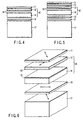
- a polarizing plate 11, a first retardation film 12, a touch panel 18, a second retardation film 15 and a liquid crystal cell 17 are arranged in the order mentioned starting with the display surface, as shown in FIG. 3.
- the polarizing plate 11 on the display side is arranged such that the polarizing axis of the polarizing plate 11 forms an angle of substantially 45° with the nx direction of the first retardation film 12.
- the resistance film type touch panel 18 used in the present invention comprises two transparent conductive substrates 13 and 14 each having a transparent conductive film 16 formed on at least one surface. These two transparent conductive substrates 13 and 14 are arranged to permit the transparent conductive films 16 to face each other.
- the resistance film type touch panel 18 is formed by arranging the first transparent conductive substrate 13 and the second transparent conductive substrate 14 in a manner to permit the transparent conductive films 16 to face each other.
- a spacer, an electrode, an insulating resin film, etc. are formed to permit the two transparent conductive substrates 13 and 14 to perform the function of the touch panel 18.
- the first transparent conductive substrate 13 can be prepared by forming the transparent conductive layer 16 on an optically isotropic film. Also, it is possible for the first transparent conductive substrate 13 to be made complex with the first retardation film 12.
- the particular construction permits decreasing the thickness of the film on the input side of the touch panel, i.e., on the side of the display surface, making it possible to maintain a small pushing force required for the touch input so as to facilitate the input.
- the second transparent conductive substrate 14 is formed of an optically isotropic material and can be prepared in general by forming the transparent conductive film 16 on a glass substrate.
- the second transparent conductive substrate 14 can be attached to the second retardation film 15.
- the transparent conductive film 16 can be formed directly on the second retardation film 15 for preparing the second transparent conductive substrate 14.
- the second retardation film 15 is arranged on the liquid crystal cell 17 below the touch panel 18, though it is possible to attach the second retardation panel 15 to the second transparent conductive substrate 14 on the lower side, which is included in the touch panel 18.
- the second retardation film 15 is arranged such that the nx direction of the second retardation film 15 is substantially parallel or perpendicular to the nx direction of the first retardation film 12.
- the liquid crystal cell 17 positioned adjacent to the second retardation film 15 it is possible for the liquid crystal cell 17 positioned adjacent to the second retardation film 15 to have a polarizing plate 21 on the electrode substrate constituting the liquid crystal cell 17, as shown in FIG. 5.
- the polarizing plate 11 arranged on the side of the display surface also performs the function of the polarizing plate on the side of the display surface of the liquid crystal display device. Therefore, it is necessary to arrange the polarizing plate 11 with attentions paid to the angle of the polarizing axis of the polarizing plate 11 relative to the liquid crystal display device.
- the retardation films 12 and 15 are arranged such that the nx directions of these retardation films 12 and 15 are perpendicular to each other, it is desirable to arrange the polarizing axis of the polarizing plate 11 on the side of the display surface in a direction equal to the direction of the polarizing axis of the polarizing plate arranged in advance on the side of the display surface of the liquid crystal display device.
- the retardation films 12 and 15 are arranged such that the nx directions are substantially equal to each other, it is desirable to arrange the polarizing plate 11 on the side of the display surface such that the polarizing axis of the polarizing plate 11 is substantially perpendicular to the polarizing axis of the polarizing plate arranged in advance on the side of the display surface of the liquid crystal display device.
- the known liquid crystal display device such as the twisted nematic (TN) type and the super twisted nematic (STN) type in the liquid crystal display device of the present invention.
- TN twisted nematic
- STN super twisted nematic
- a retardation film for color compensation is arranged in many cases between the polarizing plate 11 on the side of the display surface and the electrode substrate included in the liquid crystal cell 17.
- the retardation film for color compensation it is desirable for the retardation film for color compensation to be arranged between the second retardation film 15 and the liquid crystal cell 17 included in the liquid crystal display device of the present invention.
- liquid crystal display device of the present invention it is possible to arrange known other elements performing the function of improving the quality of the display image between the polarizing plate 11 on the side of the display surface and the liquid crystal display device in order to improve the viewing angle, the brightness, etc. of the liquid crystal display device in addition to the touch panel 18 and the retardation films 12, 15 included in the liquid crystal display device of the present invention.
- the first retardation film 12 meets the condition of nz ⁇ ny, and the second retardation film meets the condition of nz > ny in the arrangement shown in FIG. 4.
- the first retardation film 12 can be obtained by uniaxially drawing a plastic film that can be suitably used as the retardation film by a known method.
- the first retardation film 12 having the transparent conductive layer 16 formed thereon is particularly desirable to use as the first transparent conductive substrate 13 of the touch panel 18 because the particular construction permits facilitating the input of the touch panel.
- a heating step is employed in the transparent conductive processing and in the process of preparing the touch panel, making it necessary for the film substrate used to exhibit resistance to heat.
- the retardation value is changed by the heating during the processing. It follows that it is desirable to use a film having a higher resistance to heat as the retardation film among the preferred materials described previously. To be more specific, it is desirable to use a film having a glass transition temperature of at least 160°C, more preferably at least 180°C.
- the specific materials meeting the particular requirement include, for example, polyarylate, polysulfone, polyether sulfone, and polycarbonate containing at least 30 mol percent of 1,1-bis (4-hydroxyphenyl)-3,3,5-trimethyl cyclohexane as the bisphenol component.
- a sample was disposed horizontally on a stage by using a polarized microspectrophotmeter manufactured by Oak Seisakusho K.K. so as to measure the retardation (R(0)). Then, the sample was inclined by 40° in the direction of the optical axis (nx direction) so as to measure similarly the retardation (Rx(40)). The values of nx, ny, nz were calculated by using the measured values and an average refractive index (n).
- the retardation of a film cut in strips each having a width of 1 cm in the direction of the optical axis was measured by using a micropolarizing apparatus. Further, the retardation was measured by applying a load of 50g, 100g, and 150g to one end of the strip with the other end fixed, and the amount of change in the birefringence per unit stress was calculated in view of the cross sectional area of the strip of the film.
- the clarity of the transmitted image was measured in accordance with the method specified in JIS (Japanese Industrial Standards) K7105-1981.
- the light ray transmittance was measured by using a light having a wavelength of 550 nm in accordance with the method defined in ASTM E275-67.
- the haze was measured in accordance with the method specified in JIS K105-1981.
- a film made of polycarbonate comprising 1,1-bis (4-hydroxyphenyl)-3,3,5-trimethyl cyclohexane, bisphenol A (molar ratio of 4 : 6) and phosgene was coated with an epoxy acrylic ultraviolet curable coating solution having divinylbenzene series fillers having an average particle diameter of 2 ⁇ m dispersed therein, followed by curing the coating so as to obtain a hard coat layer having a thickness of about 2 ⁇ m.
- An ITO film was formed on the hard coat layer by a sputtering method so as to prepare a retardation film having a transparent conductive layer having a surface resistivity of 400 ⁇ / ⁇ .
- the clarity of the transmitted image of the substrate measured by using a slit of 0.25 mm was found to be 85%, the light ray transmittance measured by using a light having a wavelength of 550 nm was 87%, and the haze was found to be 0.8%.
- a silver electrode was printed in an edge portion of the retardation film equipped with the transparent conductive film, and a transparent conductive glass plate having spacers formed at a pitch of 5 mm and a silver electrode printed thereon, which was prepared separately, was bonded to the retardation film such that the conductive films were allowed to face each other.
- the bonding was performed by coating an insulating adhesive in the peripheral portion of each of the retardation film and the glass plate, thereby preparing a transparent touch panel.
- An additional retardation film for compensation prepared by the process equal to the process of preparing the retardation film used in the touch panel was bonded to that surface of the transparent touch panel thus prepared which is opposite to the conductive film of the transparent conductive glass plate included in the touch panel.
- These touch panel and the retardation film for compensation were arranged such that the optical axes of the retardation film of the touch panel and the retardation film for compensation (nx direction of the retardation film) were +45° and -45°, respectively ("+" representing the clockwise direction as viewed from the display side).
- the retardations were measured in a vertical direction and a direction 40° deviant from the vertical direction by using the touch panel having the retardation films made integral.
- the retardation was found to be 1 nm in the vertical direction and the measured value R'(40) in a direction 40° deviant from the vertical direction was found to be 4 nm. Therefore, the dependence of the retardation on the viewing angle was small.
- the touch panel thus prepared was incorporated in a TFT color TN liquid crystal device equipped with a back light.
- the resultant device was compared with a TFT color TN liquid crystal device in which the touch panel was not incorporated in respect of the viewing angle characteristics of the displayed image. No difference was recognized between the two.
- the retardations of the touch panel were measured in a vertical direction and in a direction 40° deviant from the vertical direction.
- the retardation measured in the vertical direction was found to be 2 nm.
- the measured value R'(40) measured in a direction 40° deviant from the vertical direction was as large as 32 nm.
- the liquid crystal display device having the touch panel incorporated therein was small in the viewing angle at which the color balance was collapsed, compared with the device in which the touch panel was not incorporated.
- the retardations of the touch panel were measured in a vertical direction and in a direction 40° deviant from the vertical direction.
- the retardation in the vertical direction was found to be 2 nm and the measured value R'(40) in a direction 40° deviant from the vertical direction was found to be 5 nm.
- Touch panels were prepared as in Example 1 by using films differing from each other in the values of nx, ny, and nz, and the viewing angle characteristics of the touch panels were measured, with the results as shown in Table 1.
- the resin used in Examples 3-7 and Comparative Example 2 was equal to that used in Example 1. Therefore, the photoelasticity coefficient was 62 ⁇ 10 -8 cm 2 /N.
- the retardations of the touch panel were measured in a vertical direction and in a direction 40° deviant from the vertical direction.
- the retardation in the vertical direction was found to be 2 nm and the retardation value R'(40) in a direction 40° deviant from the vertical direction was found to be 5 nm.
- the touch panel obtained in each of Examples 1 and 2 was made integral with a liquid crystal display device and left to stand for 250 hours under a hot and humid environment of 60°C and 90% RH.
- the unevenness in the initial retardation was found to be not larger than 5 nm in each of these panels.
- the unevenness in the retardation was increased in the touch panel for Example 2 such that the unevenness in the retardation in a plane was increased to 20 nm.
- the unevenness in the retardation was 10 nm in the touch panel for Example 1, supporting that the retardation was relatively stable under the hot and humid environment.
- the retardation of a film cut in strips each having a width of 1 cm in the direction of the optical axis was measured by using a micropolarizing apparatus. Further, the retardation was measured by applying a load of 50g, 100g, and 150g to one end of the strip with the other end fixed, and the amount of change in the birefringence per unit stress was calculated in view of the cross sectional area of the strip of the film.
- a film made of polycarbonate comprising 1,1-bis (4-hydroxyphenyl)-3,3,5-trimethyl cyclohexane, bisphenol A (molar ratio of 7 : 3) and phosgene was coated with an epoxy acrylic ultraviolet curable coating solution having divinylbenzene series fillers having an average particle diameter of 2 ⁇ m dispersed therein, followed by curing the coating so as to obtain a hard coat layer having a thickness of about 2 ⁇ m.
- An ITO film was formed on the hard coat layer by a sputtering method so as to prepare a retardation film having a transparent conductive layer having a surface resistivity of 400 ⁇ / ⁇ . The film thus prepared was used as the first retardation film shown in FIG. 4.
- a transparent touch panel was assembled by using a glass substrate having a transparent conductive layer having a surface resistivity of 200 ⁇ / ⁇ formed on the surface as a second transparent conductive substrate.
- the second retardation film was bonded with an adhesive to the surface of a transparent electrode substrate, which is made of glass, of a TFT type liquid crystal display device equipped with a back light and having the polarizing plate on the side of the display surface removed therefrom, with the nx direction aligned with the direction of 45° relative to the polarizing axis of the polarized film arranged in advance.
- a polarizing plate having an antireflection coating applied to the surface was bonded with an adhesive to the first retardation film of a touch panel such that the nx direction of the first retardation film made an angle of 45° with the polarizing axis of the polarizing plate.
- first retardation film and the second retardation film were superposed one upon the other in a manner to cross each other at right angles with spacers interposed therebetween so as to assemble a liquid crystal display device equipped with the touch panel.
- FIG. 6 shows the relative arrangement of the constituents of the liquid crystal display device equipped with the touch panel.
- the surface reflectance of the liquid crystal display device thus assembled was not higher than 1%. Where the displayed image was observed with the display surface inclined in a horizontal direction, the graduation inversion was not recognized even if the display surface was inclined by at least 60°.
- Example 10 A liquid crystal display device equipped with a touch panel was assembled as in Example 9.
- used was a film having a thickness of 75 ⁇ m and prepared by uniaxially drawing AIF75 (trade name of a polyarylate film having a glass transition temperature of 215°C and manufactured by Kanegafuchi Chemical Industries K.K.).
- Also used was a second retardation film having a thickness of 75 ⁇ m and made of polycarbonate containing bisphenol A.
- the surface reflectance of the liquid crystal display device was not higher than 1%. Also, where the displayed image was observed by inclining the surface in the horizontal direction, the graduation inversion was not recognized even if the surface was inclined by 60° or more.
- the liquid crystal display device prepared in each of Examples 9 and 10 was left to stand for 500 hours under an atmosphere having a relative humidity of 90% and temperature of 60°C. A change in color tone was not recognized in the displayed image in the liquid crystal display device for Example 9. However, a change in the color tone was partially recognized in the displayed image in the liquid crystal display device prepared in
- the present invention provides a liquid crystal display device integral with a touch panel having a high contrast and exhibiting good display quality over a wide viewing angle.
Landscapes
- Physics & Mathematics (AREA)
- Engineering & Computer Science (AREA)
- Theoretical Computer Science (AREA)
- General Engineering & Computer Science (AREA)
- Nonlinear Science (AREA)
- General Physics & Mathematics (AREA)
- Optics & Photonics (AREA)
- Crystallography & Structural Chemistry (AREA)
- Chemical & Material Sciences (AREA)
- Human Computer Interaction (AREA)
- Mathematical Physics (AREA)
- Liquid Crystal (AREA)
- Polarising Elements (AREA)
Claims (16)
- Ecran tactile transparent, comprenant :une paire de substrats conducteurs transparents (3, 4 ; 13, 14), chacun ayant un film conducteur transparent (6; 16) formé sur au moins une surface et disposé d'une telle sorte que les films conducteurs transparents (6; 16) des substrats conducteurs transparents (3, 4 ; 13, 14) peuvent se situer en regard les uns des autres, ladite paire de substrats conducteurs transparents (3, 4 ; 13, 14) étant mise en contact réciproque sur une dépression du substrat conducteur transparent sur le côté supérieur, de façon à réaliser la détection de position ; etun film retard (3 ; 12) réalisé à partir d'un matériau plastique amorphe, répondant à la relation nz > ny et ayant un retard R(0) qui est représenté par (nx - ny) x d, tombant dans une plage entre 90 nm et 200 nm, où d représente l'épaisseur dudit film retard, nx représente l'indice de réfraction maximum dans le plan du film de retard, ny représente l'indice de réfraction dans une direction perpendiculaire à nx, et nz représente l'indice de réfraction dans une direction d'épaisseur du film retard,dans lequel le coefficient de photoélasticité du film retard se situe dans une plage entre 5 × 10⁻¹ cm2/N et 65 × 10-8 cm2/N.
- Ecran tactile transparent selon la revendication 1, dans lequel ledit un film conducteur transparent (6 ; 16) est formé solidairement sur ledit film retard (3 ; 12).
- Dispositif d'affichage à cristaux liquides équipé d'un écran tactile défini dans la revendication 1 ou 2, dans lequel une couche de revêtement est formée sur au moins la surface dudit film retard (3 ; 12) sur laquelle est formé ledit film conducteur transparent (6 ; 16).
- Dispositif selon la revendication 3, dans lequel on ajoute une matière de charge à ladite couche de revêtement.
- Dispositif d'affichage à cristaux liquides équipé de l'écran tactile défini dans la revendication 1 ou 2, dans lequel la température de transition vitreuse dudit film retard est de 80°C ou au-delà.
- Dispositif d'affichage à cristaux liquides équipé d'un écran tactile, comprenant :une plaque de polarisation (1 ; 11) disposée sur le côté de la surface d'affichage ;une cellule à cristaux liquides (17) ; etl'écran tactile transparent (8 ; 18) défini dans la revendication 1 ou 2, ledit écran tactile transparent étant disposé entre la plaque de polarisation et la cellule de cristaux liquides.
- Dispositif selon la revendication 6, dans lequel un traitement antireflet est appliqué sur ladite plaque de polarisation (1 ; 11).
- Dispositif d'affichage à cristaux liquides équipé d'un écran tactile, comprenant une plaque de polarisation, un premier film retard (3 ; 12), un écran tactile (8 ; 18), un second film retard (5 ; 15) et une cellule de cristaux liquides (17), qui sont disposés dans l'ordre mentionné,
dans lequel ledit écran tactile est un écran tactile transparent du type à film à résistance,
la valeur de retard représentée par (nx - ny) x d se situe dans une plage entre 90 nm et 200 nm, où nx représente l'indice de réfraction (indice de réfraction maximum) dans la direction de l'axe de phase retardée dans les plans des premier et second films retard, ny représente l'indice de réfraction dans une direction perpendiculaire à l'axe de phase retardée, nz représente l'indice de réfraction dans la direction d'épaisseur des premier et second films retard, et d représente l'épaisseur des premier et second films retard, et
au moins l'un des premier et second films retard répond à la relation nz > ny, dans laquelle le premier film retard (3 ; 12) est réalisé à partir d'une résine ayant un coefficient de photoélasticité se situant dans une plage entre 5 x 10⁻⁸ cm2/N et 65 x 10-8 cm2/N. - Dispositif selon la revendication 8, dans lequel le premier film retard (3 ; 12) répond à la relation nz ≤ ny et le second film retard (5 ; 15) répond à la relation nz > ny.
- Dispositif selon la revendication 8 ou 9, dans lequel les premier et second films retard (3 ; 12 ; 5 ; 15) sont disposés de telle sorte que les directions nx de ces films retard sont sensiblement perpendiculaires entre elles.
- Dispositif selon la revendication 8, 9 ou 10, dans lequel les premier et second films retard sont réalisés dans le même matériau.
- Dispositif selon la revendication 8, 9, 10, ou 11, dans lequel une couche de revêtement est formée dans au moins la surface dudit premier film retard (3 ; 12) sur laquelle est formé le film conducteur transparent.
- Dispositif selon la revendication 12, dans lequel une matière de charge est ajoutée à ladite couche de revêtement.
- Dispositif selon l'une quelconque des revendications 8 à 13, dans lequel un traitement antireflet est appliqué sur ladite plaque de polarisation.
- Dispositif selon l'une quelconque des revendications 8 à 14, dans lequel une plaque de polarisation est disposée entre le second film retard (5 ; 15) et la cellule de cristaux liquides (17).
- Dispositif selon l'une quelconque des revendications 8 à 15, dans lequel la température de transition vitreuse desdits premier et second films retard est de 80°C ou au-delà.
Applications Claiming Priority (5)
| Application Number | Priority Date | Filing Date | Title |
|---|---|---|---|
| JP17152298 | 1998-06-18 | ||
| JP17152298 | 1998-06-18 | ||
| JP22034098 | 1998-08-04 | ||
| JP22034098 | 1998-08-04 | ||
| PCT/JP1999/002919 WO1999066391A1 (fr) | 1998-06-18 | 1999-06-01 | Ecran tactile transparent et affichage a cristaux liquides avec ecran tactile transparent |
Publications (3)
| Publication Number | Publication Date |
|---|---|
| EP1103885A1 EP1103885A1 (fr) | 2001-05-30 |
| EP1103885A4 EP1103885A4 (fr) | 2001-08-29 |
| EP1103885B1 true EP1103885B1 (fr) | 2006-08-16 |
Family
ID=26494223
Family Applications (1)
| Application Number | Title | Priority Date | Filing Date |
|---|---|---|---|
| EP99922626A Expired - Lifetime EP1103885B1 (fr) | 1998-06-18 | 1999-06-01 | Ecran tactile transparent et affichage a cristaux liquides avec ecran tactile transparent |
Country Status (4)
| Country | Link |
|---|---|
| US (1) | US6411344B2 (fr) |
| EP (1) | EP1103885B1 (fr) |
| DE (1) | DE69932826T2 (fr) |
| WO (1) | WO1999066391A1 (fr) |
Cited By (1)
| Publication number | Priority date | Publication date | Assignee | Title |
|---|---|---|---|---|
| TWI408591B (zh) * | 2009-10-06 | 2013-09-11 | Wintek Corp | 觸控顯示面板 |
Families Citing this family (70)
| Publication number | Priority date | Publication date | Assignee | Title |
|---|---|---|---|---|
| JP2000207128A (ja) * | 1999-01-18 | 2000-07-28 | Matsushita Electric Ind Co Ltd | 透明タッチパネルおよびそれを用いた電子機器 |
| US7030860B1 (en) * | 1999-10-08 | 2006-04-18 | Synaptics Incorporated | Flexible transparent touch sensing system for electronic devices |
| JP2001290135A (ja) * | 2000-01-31 | 2001-10-19 | Nitto Denko Corp | タッチ式液晶表示装置及び入力検出方法 |
| JP2002041231A (ja) * | 2000-05-17 | 2002-02-08 | Hitachi Ltd | 画面入力型表示装置 |
| US6787240B2 (en) * | 2000-06-23 | 2004-09-07 | Donnelly Corporation | Enhanced light transmission conductive coated transparent substrate |
| US6771327B2 (en) * | 2000-09-18 | 2004-08-03 | Citizen Watch Co., Ltd. | Liquid crystal display device with an input panel |
| JP2002107541A (ja) * | 2000-10-02 | 2002-04-10 | Nitto Denko Corp | 光学シート、偏光板及び液晶表示装置 |
| KR100474750B1 (ko) | 2000-10-13 | 2005-03-10 | 가부시키가이샤 덴소 | 터치 패널, 표시장치, 및 터치 패널의 제조방법 |
| JP4566385B2 (ja) * | 2000-10-30 | 2010-10-20 | 日東電工株式会社 | 偏光板 |
| JP4566384B2 (ja) | 2000-10-30 | 2010-10-20 | 日東電工株式会社 | 偏光板 |
| JP2002148434A (ja) | 2000-11-08 | 2002-05-22 | Nitto Denko Corp | 偏光板 |
| JP2003050674A (ja) * | 2001-08-08 | 2003-02-21 | Nagano Fujitsu Component Kk | タッチパネル及びタッチパネルを備えた入力装置 |
| CN1301510C (zh) * | 2001-10-05 | 2007-02-21 | 普利司通股份有限公司 | 透明导电性薄膜、其制造方法以及触摸面板 |
| JP2003271311A (ja) * | 2002-03-18 | 2003-09-26 | Alps Electric Co Ltd | 座標入力装置およびこれを用いた液晶表示装置 |
| EP1496376B1 (fr) * | 2002-03-25 | 2011-06-15 | Zeon Corporation | Film optique et son procede de production |
| US6777869B2 (en) | 2002-04-10 | 2004-08-17 | Si Diamond Technology, Inc. | Transparent emissive display |
| EP1387210A1 (fr) * | 2002-08-02 | 2004-02-04 | Eastman Kodak Company | Couche compensatrice et dispositif à cristaux liquides comportant une telle couche |
| US7583326B2 (en) | 2002-08-20 | 2009-09-01 | Samsung Electronics Co., Ltd. | Light guide plate and liquid crystal display having the same |
| WO2004019119A1 (fr) * | 2002-08-20 | 2004-03-04 | Samsung Electronics Co., Ltd. | Connecteur optique plat et affichage a cristaux liquides le comportant |
| US7936338B2 (en) | 2002-10-01 | 2011-05-03 | Sony Corporation | Display unit and its manufacturing method |
| CN1316294C (zh) * | 2002-12-10 | 2007-05-16 | 统宝光电股份有限公司 | 结合触控面板的平面显示器 |
| US7833588B2 (en) | 2002-12-20 | 2010-11-16 | Teijin Limited | Transparent conductive laminate, touch panel and touch panel-equipped liquid crystal display |
| CN100397531C (zh) * | 2003-02-03 | 2008-06-25 | 普利司通股份有限公司 | 透明导电性膜、透明导电板和触摸面板 |
| US6909486B2 (en) * | 2003-02-18 | 2005-06-21 | Ran-Hong Raymond Wang | Liquid crystal display viewable under all lighting conditions |
| JP4507505B2 (ja) * | 2003-04-09 | 2010-07-21 | ソニー株式会社 | 液晶表示装置 |
| US7211304B2 (en) * | 2004-06-03 | 2007-05-01 | Nitto Denko Corporation | Multilayer optical compensator, liquid crystal display, and process |
| US7479309B2 (en) * | 2003-07-31 | 2009-01-20 | Nitto Denko Corporation | Multi-layered compensation film using specified Tg material as a birefringent layer |
| US8400430B2 (en) * | 2003-11-21 | 2013-03-19 | American Panel Corporation | Display device with integral touch panel surface |
| CN100374916C (zh) * | 2003-12-24 | 2008-03-12 | 胜华科技股份有限公司 | 具光学胶耦合的五线式塑料触控显示器 |
| US20080088601A1 (en) * | 2004-05-19 | 2008-04-17 | Tpk Touch Solutions Inc. | Circuit layout on a touch panel |
| US7288296B2 (en) * | 2004-06-03 | 2007-10-30 | Nitto Denko Corporation | Multilayer optical compensator, liquid crystal display, and process |
| US20060001655A1 (en) * | 2004-07-01 | 2006-01-05 | Koji Tanabe | Light-transmitting touch panel and detection device |
| DE102006023993A1 (de) * | 2005-05-23 | 2007-03-08 | Wang, Ran-Hong, Tustin | Polarisationssteuerung für Flüssigkristallanzeigen |
| US7633583B2 (en) * | 2005-05-23 | 2009-12-15 | Ran-Hong Raymond Wang | Controlling polarization for liquid crystal displays |
| KR20070059293A (ko) * | 2005-12-06 | 2007-06-12 | 삼성전자주식회사 | 액정 표시 장치, 이를 위한 표시판 및 그 제조 방법 |
| US8144115B2 (en) | 2006-03-17 | 2012-03-27 | Konicek Jeffrey C | Flat panel display screen operable for touch position determination system and methods |
| US7859526B2 (en) * | 2006-05-01 | 2010-12-28 | Konicek Jeffrey C | Active matrix emissive display and optical scanner system, methods and applications |
| EP1898252B1 (fr) * | 2006-09-05 | 2014-04-30 | Tosoh Corporation | Empilement de films de compensation optique et film étiré à retard optique |
| US20080088595A1 (en) * | 2006-10-12 | 2008-04-17 | Hua Liu | Interconnected two-substrate layer touchpad capacitive sensing device |
| US8072429B2 (en) * | 2006-12-22 | 2011-12-06 | Cypress Semiconductor Corporation | Multi-axial touch-sensor device with multi-touch resolution |
| JP2008204321A (ja) * | 2007-02-22 | 2008-09-04 | Matsushita Electric Ind Co Ltd | 入力装置 |
| EP2179311B1 (fr) * | 2007-08-14 | 2015-09-16 | LG Chem, Ltd. | Film optique et son procédé de fabrication |
| TW200933238A (en) * | 2008-01-28 | 2009-08-01 | Delta Electronics Inc | Touch panel |
| JP4831778B2 (ja) * | 2008-03-05 | 2011-12-07 | 日東電工株式会社 | タッチパネル |
| CN101952794A (zh) * | 2008-03-14 | 2011-01-19 | 夏普株式会社 | 区域传感器和带区域传感器的显示装置 |
| TWI402728B (zh) * | 2009-02-24 | 2013-07-21 | Wintek Corp | 觸控面板及觸控式顯示面板 |
| TWI416383B (zh) * | 2009-03-16 | 2013-11-21 | Wintek Corp | 觸控面板與液晶顯示面板 |
| US8174510B2 (en) | 2009-03-29 | 2012-05-08 | Cypress Semiconductor Corporation | Capacitive touch screen |
| US9753597B2 (en) | 2009-07-24 | 2017-09-05 | Cypress Semiconductor Corporation | Mutual capacitance sensing array |
| US20110018829A1 (en) * | 2009-07-24 | 2011-01-27 | Cypress Semiconductor Corporation | Mutual capacitance sensing array |
| KR20110110593A (ko) * | 2010-04-01 | 2011-10-07 | 삼성모바일디스플레이주식회사 | 평판 표시 장치 |
| US7876288B1 (en) | 2010-08-11 | 2011-01-25 | Chumby Industries, Inc. | Touchscreen with a light modulator |
| KR101706946B1 (ko) * | 2010-06-14 | 2017-02-15 | 엘지전자 주식회사 | 터치 패널 디스플레이 장치 |
| TW201335669A (zh) * | 2012-02-20 | 2013-09-01 | Innocom Tech Shenzhen Co Ltd | 觸控顯示裝置及其製造方法 |
| TW201337349A (zh) * | 2012-03-12 | 2013-09-16 | Innocom Tech Shenzhen Co Ltd | 光學構件及顯示系統 |
| US8946985B2 (en) | 2012-05-07 | 2015-02-03 | Samsung Display Co., Ltd. | Flexible touch screen panel and flexible display device with the same |
| TWI486835B (zh) | 2012-05-08 | 2015-06-01 | Htc Corp | 觸控顯示裝置 |
| KR101919107B1 (ko) * | 2012-05-08 | 2018-11-16 | 삼성디스플레이 주식회사 | 표시 장치 |
| WO2014075804A1 (fr) * | 2012-11-15 | 2014-05-22 | SÜDDEKOR GmbH | Matière de surface pour le revêtement de stratifiés en résine de mélamine |
| EP2952940B1 (fr) * | 2013-02-01 | 2019-05-22 | Murata Manufacturing Co., Ltd. | Panneau d'affichage muni d'un capteur de pression, et dispositif électronique doté d'une fonction d'entrée de pression |
| JP2014219667A (ja) * | 2013-04-04 | 2014-11-20 | 日東電工株式会社 | 導電性フィルムおよび画像表示装置 |
| KR101401050B1 (ko) * | 2013-08-09 | 2014-06-27 | 동우 화인켐 주식회사 | 터치 감지 전극 및 이를 포함하는 터치 스크린 패널 |
| KR101443689B1 (ko) * | 2013-08-23 | 2014-09-23 | 동우 화인켐 주식회사 | 편광판 일체형 터치 감지 전극 |
| KR101444132B1 (ko) * | 2013-11-20 | 2014-11-04 | 동우 화인켐 주식회사 | 복합 편광판 일체형 터치 감지 전극 및 이를 구비한 터치 스크린 패널 |
| US20170147098A1 (en) * | 2014-04-03 | 2017-05-25 | Sekisui Chemical Co., Ltd. | Interlayer filling material for touch panel, and laminated body |
| JP2016114906A (ja) * | 2014-12-18 | 2016-06-23 | 日東電工株式会社 | 偏光板、及び画像表示装置 |
| KR20180068948A (ko) * | 2015-10-07 | 2018-06-22 | 세키스이가가쿠 고교가부시키가이샤 | 터치 패널용 층간 충전 재료 및 터치 패널 적층체 |
| JP7044468B2 (ja) * | 2016-02-05 | 2022-03-30 | 三菱ケミカル株式会社 | 光学積層体および該光学積層体を用いた画像表示装置 |
| US10795197B2 (en) * | 2018-08-24 | 2020-10-06 | Sharp Kabushiki Kaisha | Liquid crystal panel |
| CN111200001A (zh) * | 2020-01-10 | 2020-05-26 | 京东方科技集团股份有限公司 | 一种显示面板和显示装置 |
Family Cites Families (24)
| Publication number | Priority date | Publication date | Assignee | Title |
|---|---|---|---|---|
| JPH0215238A (ja) * | 1988-07-04 | 1990-01-18 | Stanley Electric Co Ltd | 異方性補償ホメオトロピック液晶表示装置 |
| JP2857889B2 (ja) * | 1988-11-04 | 1999-02-17 | 富士写真フイルム株式会社 | 液晶表示装置 |
| JP2612196B2 (ja) * | 1988-12-14 | 1997-05-21 | 富士写真フイルム株式会社 | 位相差フイルム及びその製造方法 |
| JPH02285303A (ja) * | 1989-04-26 | 1990-11-22 | Nitto Denko Corp | 複屈折性フィルム及びその製造方法並びに位相差板及び液晶パネル |
| US4985285A (en) * | 1989-04-26 | 1991-01-15 | Fujimori Kogyo Co., Ltd. | Liquid crystal display panel incorporating an optical phase shifting substrate |
| JP2809712B2 (ja) * | 1989-06-22 | 1998-10-15 | 株式会社クラレ | 位相差板 |
| JP3094113B2 (ja) * | 1990-05-25 | 2000-10-03 | 住友化学工業株式会社 | 位相差板およびその製造方法 |
| JP2818983B2 (ja) * | 1990-10-24 | 1998-10-30 | 日東電工株式会社 | 複屈折性フィルムの製造方法 |
| WO1992022835A1 (fr) * | 1991-06-17 | 1992-12-23 | Seiko Epson Corporation | Couche mince elementaire a difference de phase, plaque a difference de phase et affichage a cristaux liquide |
| JPH05127822A (ja) * | 1991-10-30 | 1993-05-25 | Daicel Chem Ind Ltd | タツチパネル |
| JPH06337421A (ja) * | 1993-05-31 | 1994-12-06 | Toshiba Corp | 反射型液晶表示素子 |
| JP3019741B2 (ja) * | 1994-02-24 | 2000-03-13 | ジェイエスアール株式会社 | 位相板 |
| EP0740181B1 (fr) * | 1994-10-26 | 2004-10-13 | Seiko Epson Corporation | Dispositif a cristaux liquides et appareil electronique |
| DE69630829T2 (de) * | 1995-02-02 | 2004-09-23 | Teijin Ltd. | Transparentes leitfähiges Flächenmaterial |
| JPH08281856A (ja) * | 1995-04-12 | 1996-10-29 | Nippon Paper Ind Co Ltd | 透明導電性フィルム又はシート |
| JPH09237159A (ja) * | 1995-12-13 | 1997-09-09 | Gunze Ltd | 抵抗膜型透明タッチパネル |
| JPH09203890A (ja) * | 1996-01-25 | 1997-08-05 | Sharp Corp | 入力機能付き液晶表示素子および反射型入力機能付き液晶表示素子、並びにそれらの製造方法 |
| EP0789295B1 (fr) * | 1996-02-09 | 2003-05-02 | Seiko Instruments Inc. | Unité d'affichage avec un commutateur tactile transparent et un affichage à cristaux liquides, et procédé de fabrication |
| US5833878A (en) * | 1996-02-14 | 1998-11-10 | Jsr Corporation | Liquid crystal display panel |
| JP3198046B2 (ja) * | 1996-03-14 | 2001-08-13 | 株式会社リコー | 入力タッチパネル付き液晶表示装置 |
| JPH1048625A (ja) * | 1996-08-02 | 1998-02-20 | Sumitomo Chem Co Ltd | 液晶ディスプレイ用タッチパネル |
| JP3854392B2 (ja) * | 1996-11-11 | 2006-12-06 | 同和鉱業株式会社 | 光学的フィルター |
| JPH10260403A (ja) * | 1997-01-20 | 1998-09-29 | Seiko Epson Corp | 液晶装置及び電子機器 |
| JPH11109335A (ja) * | 1997-09-30 | 1999-04-23 | Sharp Corp | 液晶表示装置 |
-
1999
- 1999-06-01 DE DE69932826T patent/DE69932826T2/de not_active Expired - Fee Related
- 1999-06-01 EP EP99922626A patent/EP1103885B1/fr not_active Expired - Lifetime
- 1999-06-01 WO PCT/JP1999/002919 patent/WO1999066391A1/fr not_active Ceased
-
2000
- 2000-12-15 US US09/741,286 patent/US6411344B2/en not_active Expired - Lifetime
Cited By (1)
| Publication number | Priority date | Publication date | Assignee | Title |
|---|---|---|---|---|
| TWI408591B (zh) * | 2009-10-06 | 2013-09-11 | Wintek Corp | 觸控顯示面板 |
Also Published As
| Publication number | Publication date |
|---|---|
| WO1999066391A1 (fr) | 1999-12-23 |
| US6411344B2 (en) | 2002-06-25 |
| US20010008433A1 (en) | 2001-07-19 |
| DE69932826T2 (de) | 2006-12-14 |
| EP1103885A1 (fr) | 2001-05-30 |
| EP1103885A4 (fr) | 2001-08-29 |
| DE69932826D1 (en) | 2006-09-28 |
Similar Documents
| Publication | Publication Date | Title |
|---|---|---|
| EP1103885B1 (fr) | Ecran tactile transparent et affichage a cristaux liquides avec ecran tactile transparent | |
| EP1574882B1 (fr) | Lamine conducteur transparent, ecran tactile et unite d'affichage a cristaux liquides dotee d'un ecran tactile | |
| EP1020755B1 (fr) | Dispositif d'affichage a cristaux liquides a ecran tactile | |
| JP4177557B2 (ja) | 液晶表示装置に使用するための抵抗膜方式のタッチパネルおよびこれを備えた液晶表示装置 | |
| EP1045261B1 (fr) | Film a differences de phase et dispositif optique dans lequel il est utilise | |
| US7012663B2 (en) | Liquid crystal display element, and use of phase difference film used the same for | |
| US7130007B2 (en) | Optical film, polarizing optical film, and image viewing display | |
| US6937310B2 (en) | Compensation films for LCDs | |
| US7223451B2 (en) | Polycarbonate-based oriented film and retardation film | |
| EP1826608A1 (fr) | Affichage à cristaux liquides | |
| JP2000112663A (ja) | 透明タッチパネルおよび透明タッチパネル付液晶セル | |
| JP2000111896A (ja) | タッチパネル付き液晶表示装置及びタッチパネル | |
| JP3663783B2 (ja) | 液晶表示装置 | |
| JPH03120037A (ja) | 積層体の干渉縞発生防止方法及び干渉縞の発生を防止した積層体 | |
| JP2000206531A (ja) | タッチパネル付き液晶表示装置及びタッチパネル | |
| JP2001201632A (ja) | タッチパネル付き液晶表示装置及びタッチパネル | |
| JP3511867B2 (ja) | 液晶表示装置 | |
| CN115485593A (zh) | 偏光板及带光学功能层的偏光板 | |
| JPH09318816A (ja) | 光学フィルム、その製造方法、積層偏光板及び液晶表示装置 | |
| JPWO1999066391A1 (ja) | 透明タッチパネル及び透明タッチパネル付き液晶表示装置 | |
| JP2000056301A (ja) | 光学装置 | |
| KR20060055389A (ko) | 노멀리 화이트 tn 모드의 lcd 장치 | |
| JPH11249812A (ja) | 透明タッチパネル付液晶セル | |
| JP2002055780A (ja) | タッチパネル及びタッチパネル付表示装置 | |
| JP2004341561A (ja) | 液晶表示装置 |
Legal Events
| Date | Code | Title | Description |
|---|---|---|---|
| PUAI | Public reference made under article 153(3) epc to a published international application that has entered the european phase |
Free format text: ORIGINAL CODE: 0009012 |
|
| 17P | Request for examination filed |
Effective date: 20010103 |
|
| AK | Designated contracting states |
Kind code of ref document: A1 Designated state(s): DE FR GB |
|
| A4 | Supplementary search report drawn up and despatched |
Effective date: 20010718 |
|
| AK | Designated contracting states |
Kind code of ref document: A4 Designated state(s): DE FR GB |
|
| RIC1 | Information provided on ipc code assigned before grant |
Free format text: 7G 06F 3/033 A, 7G 02F 1/133 B, 7G 02F 1/1335 B, 7G 06K 11/12 B, 7G 02F 1/13 B |
|
| 17Q | First examination report despatched |
Effective date: 20050310 |
|
| GRAP | Despatch of communication of intention to grant a patent |
Free format text: ORIGINAL CODE: EPIDOSNIGR1 |
|
| RIC1 | Information provided on ipc code assigned before grant |
Ipc: G02F 1/13 20060101ALI20060130BHEP Ipc: G02F 1/1335 20060101ALI20060130BHEP Ipc: G02F 1/133 20060101ALI20060130BHEP Ipc: G06F 3/033 20060101AFI20060130BHEP |
|
| GRAS | Grant fee paid |
Free format text: ORIGINAL CODE: EPIDOSNIGR3 |
|
| GRAA | (expected) grant |
Free format text: ORIGINAL CODE: 0009210 |
|
| AK | Designated contracting states |
Kind code of ref document: B1 Designated state(s): DE FR GB |
|
| REG | Reference to a national code |
Ref country code: GB Ref legal event code: FG4D |
|
| REF | Corresponds to: |
Ref document number: 69932826 Country of ref document: DE Date of ref document: 20060928 Kind code of ref document: P |
|
| EN | Fr: translation not filed | ||
| PLBE | No opposition filed within time limit |
Free format text: ORIGINAL CODE: 0009261 |
|
| STAA | Information on the status of an ep patent application or granted ep patent |
Free format text: STATUS: NO OPPOSITION FILED WITHIN TIME LIMIT |
|
| 26N | No opposition filed |
Effective date: 20070518 |
|
| GBPC | Gb: european patent ceased through non-payment of renewal fee |
Effective date: 20070601 |
|
| PG25 | Lapsed in a contracting state [announced via postgrant information from national office to epo] |
Ref country code: FR Free format text: LAPSE BECAUSE OF FAILURE TO SUBMIT A TRANSLATION OF THE DESCRIPTION OR TO PAY THE FEE WITHIN THE PRESCRIBED TIME-LIMIT Effective date: 20070511 |
|
| PG25 | Lapsed in a contracting state [announced via postgrant information from national office to epo] |
Ref country code: GB Free format text: LAPSE BECAUSE OF NON-PAYMENT OF DUE FEES Effective date: 20070601 |
|
| PGFP | Annual fee paid to national office [announced via postgrant information from national office to epo] |
Ref country code: DE Payment date: 20080605 Year of fee payment: 10 |
|
| PG25 | Lapsed in a contracting state [announced via postgrant information from national office to epo] |
Ref country code: FR Free format text: LAPSE BECAUSE OF FAILURE TO SUBMIT A TRANSLATION OF THE DESCRIPTION OR TO PAY THE FEE WITHIN THE PRESCRIBED TIME-LIMIT Effective date: 20060816 |
|
| PG25 | Lapsed in a contracting state [announced via postgrant information from national office to epo] |
Ref country code: DE Free format text: LAPSE BECAUSE OF NON-PAYMENT OF DUE FEES Effective date: 20100101 |