EP1104013A2 - Fortgeschrittene Metall-Halbleiterscheibenplanarisierung mit Hilfe von Elektropolieren - Google Patents
Fortgeschrittene Metall-Halbleiterscheibenplanarisierung mit Hilfe von Elektropolieren Download PDFInfo
- Publication number
- EP1104013A2 EP1104013A2 EP00310560A EP00310560A EP1104013A2 EP 1104013 A2 EP1104013 A2 EP 1104013A2 EP 00310560 A EP00310560 A EP 00310560A EP 00310560 A EP00310560 A EP 00310560A EP 1104013 A2 EP1104013 A2 EP 1104013A2
- Authority
- EP
- European Patent Office
- Prior art keywords
- substrate
- polishing
- anode
- electrolyte solution
- spots
- Prior art date
- Legal status (The legal status is an assumption and is not a legal conclusion. Google has not performed a legal analysis and makes no representation as to the accuracy of the status listed.)
- Withdrawn
Links
Images


Classifications
-
- H—ELECTRICITY
- H10—SEMICONDUCTOR DEVICES; ELECTRIC SOLID-STATE DEVICES NOT OTHERWISE PROVIDED FOR
- H10P—GENERIC PROCESSES OR APPARATUS FOR THE MANUFACTURE OR TREATMENT OF DEVICES COVERED BY CLASS H10
- H10P52/00—Grinding, lapping or polishing of wafers, substrates or parts of devices
- H10P52/40—Chemomechanical polishing [CMP]
- H10P52/403—Chemomechanical polishing [CMP] of conductive or resistive materials
-
- H—ELECTRICITY
- H10—SEMICONDUCTOR DEVICES; ELECTRIC SOLID-STATE DEVICES NOT OTHERWISE PROVIDED FOR
- H10P—GENERIC PROCESSES OR APPARATUS FOR THE MANUFACTURE OR TREATMENT OF DEVICES COVERED BY CLASS H10
- H10P95/00—Generic processes or apparatus for manufacture or treatments not covered by the other groups of this subclass
- H10P95/04—Planarisation of conductive or resistive materials
Definitions
- This invention relates generally to planarization of metal substrates and more particularly to advanced electrolytic polishing of metal films on semiconductor wafers.
- Integrated circuits are typically formed on substrates, particularly silicon wafers, by the sequential deposition of conductive,, semiconductive or insulative layers. After a layer is deposited, the layer is etched to create circuitry features. As a series of layers are sequentially deposited and etched, the outer or uppermost surface of the substrate, i.e., the exposed surface of the substrate, becomes increasingly non-planar. This non-planar outer surface presents a problem for the integrated circuit manufacturer. Therefore, there is a need to periodically planarize the substrate surface to provide a relatively flat surface. In some fabrication processes, planarization of the outer layer should not expose underlying layers.
- CMP Chemical mechanical polishing
- This planarization method typically requires that the substrate be mounted on a carrier or polishing head. The exposed surface of the substrate is placed against a rotating polishing pad.
- the polishing pad may be either a "standard” pad or a fixed-abrasive pad.
- a fixed-abrasive pad has abrasive particles held in a containment media, whereas a standard pad has a durable surface, without embedded abrasive particles.
- the carrier head provides a controllable load, i.e., pressure, on the substrate to push it against the polishing pad.
- a polishing slurry, including at least one chemically-reactive agent, and abrasive particles if a standard pad is used, is supplied to the surface of the polishing pad.
- An effective CMP process not only provides a high polishing rate, but also provides a substrate surface which is finished and flat.
- the polishing rate, finish and flatness are determined by the pad and slurry combination, the relative speed between the substrate and pad, and the force pressing the substrate against the pad.
- a dense array of metal features is typically formed in an interlayer dielectric, such as silicon oxide layer, by a damascene technique wherein trenches are initially formed.
- a barrier layer such as a Ta-containing layer e.g. Ta, TaN, is then deposited lining the trenches and on the upper surface of the silicon oxide interlayer dielectric.
- Copper or a copper alloy is then deposited, as by electroplating, electroless plating, physical vapor deposition (PVD) at a temperature of about 50°C to about 150°C or chemical vapor deposition (CVD) at a temperature under about 200°C, typically at a thickness of about 8000 ⁇ to about 18,000 ⁇ .
- PVD physical vapor deposition
- CVD chemical vapor deposition
- undesirable erosion and dishing typically occur, decreasing the degree of surface uniformity or planarity and challenging the depth of focus limitations of conventional photolithographic techniques, particular with i respect to achieving submicron dimensions, such as about 0.25 micron.
- Erosion is defined as the height differential between the oxide in the open field and the height of the oxide within the dense array.
- Dishing is defined as a difference in height between the oxide and Cu within the dense array.
- Dishing and erosion formation are the most important parameters in evaluating metal CMP processes. Current processes using CMP generate at best 600-800 ⁇ dishing and 400
- AEP advanced electrolytic polish
- the advanced electrolytic polish (AEP) method polishes the metal surface of a layered substrate in a controlled way so that higher spots are removed more quickly than lower spots in the surface topography.
- AEP uses a reverse electroplating method along with surface modifying methods, either alone or in combination, to remove material from a substrate in order to planarize the substrate.
- a first surface modifying method is to include surface modifying additives in the electrolyte solution used for AEP.
- a second surface modifying method is pulsed electrolysis with application of alternating positive and negative potentials, in which the potential across the electrodes in AEP is periodically reversed causing high points on the substrate surface to be removed before low points on the substrate surface. Additives and pulsed electrolysis can be combined in an AEP process.
- the polish in the present embodiment of the invention stops when a barrier layer (e.g.tantalum, tantalum nitride, titanium or titanium nitride) is substantially removed.
- a barrier layer e.g.tantalum, tantalum nitride, titanium or titanium nitride
- Alteration of the electrolyte chemistry of the present invention would alter the depth and the layers removed in the polish.
- Additives to the electrolyte solution, and the application of pulsed voltage during electrolytic polish further improve the planarity of the substrate polished surface.
- substrates act as anodic electrodes and another metal plate is used as a cathodic electrode.
- the substrate and the cathode are configured in either an electroplating tank or in an adapted chemical mechanical polishing device.
- a voltage differential is applied to the anode and cathode under a predetermined anodic dissolution current density. This causes a reaction that provides a planarized surface on the metal wafers.
- Current electrolytic polishing methods generally leave at least 500A difference between high and low spots in the wafer surface topography. With the present advanced electrolytic polish, additives are included in the electrolyte solution which adsorb onto the wafer surface urging a higher removal rate at higher spots and a lower removal rate at lower spots.
- another embodiment of the present invention is a pulsed-electrolytic process in which positive and negative potentials are applied to the anodic and cathodic electrodes alternately, further encouraging surface planarization.
- a further embodiment of the invention involves using the additive method and the pulsed method in combination.
- AEP can be used either as a first step followed by a short mechanical polishing step (buffing) to remove the thin barrier layer (250 ⁇ ); or as a second step between an initial CMP polish with about 2000 ⁇ copper layer remaining and a third step mechanical polish.
- the present invention may also be added as a last step of copper electroplating process and so may be used in the manufacture of all kinds of patterned metal wafers.
- the AEP technique With the AEP technique, the "insufficient planarization" problem that occurs in normal CMP processes is substantially eliminated, the first CMP step is much easier, and dishing and erosion caused by the over-polishing step are avoided.
- AEP eliminates erosion because there is no mechanical action during the AEP process. This is particularly important in processing wafers having high density surface patterns where there is a high potential for erosion. Dishing is greatly decreased with the chemical additives and the pulsed current.
- the AEP method provides a planarized surface without erosion and with very little dishing.
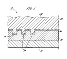
- Figure 1 shows a cross-sectional view of a conductive substrate 10 having deposited layers such as those layers formed during the manufacture of semiconductors.
- An interlayer dielectric 20, e.g. silicon oxide, is formed overlying a metal wafer 15.
- a plurality of indentations, also referred to as openings 25, are formed in a designated area at the left of the interlayer dielectric 20 in which a dense array of conductive lines are to be formed bordering an open field shown on the right of the interlayer dielectric 20.
- a conductive layer 35 e.g. copper, is then deposited over the barrier layer 30.
- the successive layers forms an uneven topography 36 over the substrate which requires planarization before further processing. Also, successive process steps require that portions of the conductive layer be removed. Planarization and selective removal of the conductive layer are accomplished in a polishing step.
- FIG. 2 shows a side cross-sectional view of an electrolyzer in a first embodiment of the present invention of advanced electrolytic polishing (AEP).
- AEP advanced electrolytic polishing
- the conductive substrate 10 of Figure 1 is immersed in a tank 50 containing a solution 55 of electrolytes.
- the conductive substrate 10 is connected to a conductive clamp 60 to form a first electrode, an anode.
- a second electrode 65, a cathode matching the metal substrate is also immersed in the tank 50.
- a voltage differential is applied to the anode and cathode under a predetermined anodic dissolution current density.
- the current density is typically 1 - 30 mA/cm 2 .
- This causes a reaction that provides a planarized surface on conductive substrates.
- the reaction when the barrier layer is substantially exposed, leaving a planarized surface on the substrate having conductive areas and substantially exposed barrier layer.
- Current electrolytic polishing methods generally leave at least 500 ⁇ difference between high and low spots in the wa
- Additives are included in the electrolyte solution which adsorb onto the substrate surface urging a higher removal rate at higher spots and a lower removal rate at lower spots.
- the additives are generally less than 1% of the electrolyte solution by weight.
- the additives are surface modifiers.
- the adsorbed additives act as electric discharge points that modify the surface of the substrate so that high spots are polished first and then low spots are polished.
- Other additives and concentrations are possible within the scope of the present invention.
- a pulsed-electrolytic process is applied, using a pulse apparatus 70, in which positive and negative potentials are applied between the anodic and cathodic electrodes alternately, further encouraging surface planarization.
- the pulse apparatus may be an alternator, or a potentiostat with pulsing capability.
- a current density typically in the range of 1 - 30 mA/cm 2 , for example, is applied typically for a few milliseconds.
- the pulse-polish modifies the surface of the substrate. Material from high spots on the surface is redeposited to low spots on the surface. This is a useful surface modification in those cases where planarization is not sufficient.
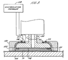
- Figure 3 shows a simplified, part cross-sectional, part schematic, side view of an even further embodiment of the present invention of AEP.
- a polish head 100 rests on a polish pad 105 with the metal substrate 10 of Figure 1 in between the head 100 and the pad 105.
- An anodic connection 110 and a cathodic connection 115 are provided.
- the anodic connection contacts the substrate 10 such that the substrate becomes an anode.
- the anodic 110 and cathodic 115 connections form rings around the head inside the retaining ring 120.
- a membrane 118 between the polish head and the substrate 10 provides pressure to maintain the contact between the anodic connection 110 and the substrate 10 and between the substrate 10 and polish pad 105.
- First 116 and second 117 brushes provide electrical connection from connections 110, 115 to an electrolysis controller 119.
- the electrolysis controller 119 may include a pulse apparatus 70 such as that shown in Figure 2.
- a metal portion of the retaining ring 120 acts as a cathode 122.
- the placement of anodes 110, 115 and the cathode 122 are merely exemplary. Other configurations are possible within the scope of the present invention.
- the pad 105 is wetted with electrolyte solution 121.
- a slurry arm 225 (shown in Figure 4) having tubes for slurry, in this case for electrolyte solution, extends over the polishing pad 105.
- a voltage differential is applied to the anode substrate 10 and the cathode 122. This causes a reaction that provides a planarized surface on the conductive substrate.
- the head 100 spins in order to carry polishing product away from the wafer 10, however, mechanical polishing does not take place.
- Additives are added to the electrolyte solution with the same effect as described above. No abrasion of the wafer is necessary in order to accomplish the polishing.
- the pulse polish technique may also be used in this configuration.
- Figure 4 shows a chemical mechanical polishing apparatus 200 having a plurality of polishing stations 205, 210, 215.
- One of the polish heads on the apparatus 200 has modifications as shown in Figure 3 in order to accomplish the present invention.
- the head 220 of polishing station 205 has an anodic connection 110, and a cathode 122 as seen in Figure 3.
- Slurry arm 225 delivers electrolyte solution to the polishing pad 105.
- one or more of the polishing stations could be modified with the electrochemical cell shown in Figure 2 in order to accomplish the present invention.
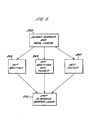
- FIG. 5 is a flow chart of a first embodiment of a polishing step using AEP according to principles of the present invention.
- AEP is applied to planarize the wafer.
- the planarization may be accomplished by AEP using additives, block 255, AEP using pulsed current, block 260, or AEP using both additives and pulsed current, block 265.
- CMP is applied to the wafer to remove the barrier layer, block 270.
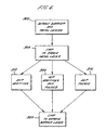
- FIG. 6 is a flow chart of a second embodiment of a polishing step using AEP according to principles of the present invention.
- CMP is applied, block 305, until a thin film of metal of a predetermined thickness remains, for example 2000 ⁇ .
- AEP is applied to remove the remaining metal and to planarize the surface of the wafer.
- the AEP process may be AEP using i additives, block 310, AEP using pulsed current, block 315, or AEP using both additives and pulsed current, block 320.
- CMP is then applied to the wafer to remove the barrier layer, block 325.
Landscapes
- Mechanical Treatment Of Semiconductor (AREA)
- Finish Polishing, Edge Sharpening, And Grinding By Specific Grinding Devices (AREA)
- Weting (AREA)
- Electroplating Methods And Accessories (AREA)
- Electrical Discharge Machining, Electrochemical Machining, And Combined Machining (AREA)
Applications Claiming Priority (2)
| Application Number | Priority Date | Filing Date | Title |
|---|---|---|---|
| US450858 | 1982-12-17 | ||
| US09/450,858 US6299741B1 (en) | 1999-11-29 | 1999-11-29 | Advanced electrolytic polish (AEP) assisted metal wafer planarization method and apparatus |
Publications (2)
| Publication Number | Publication Date |
|---|---|
| EP1104013A2 true EP1104013A2 (de) | 2001-05-30 |
| EP1104013A3 EP1104013A3 (de) | 2004-04-14 |
Family
ID=23789786
Family Applications (1)
| Application Number | Title | Priority Date | Filing Date |
|---|---|---|---|
| EP00310560A Withdrawn EP1104013A3 (de) | 1999-11-29 | 2000-11-29 | Fortgeschrittene Metall-Halbleiterscheibenplanarisierung mit Hilfe von Elektropolieren |
Country Status (3)
| Country | Link |
|---|---|
| US (2) | US6299741B1 (de) |
| EP (1) | EP1104013A3 (de) |
| JP (1) | JP2001203179A (de) |
Cited By (7)
| Publication number | Priority date | Publication date | Assignee | Title |
|---|---|---|---|---|
| WO2002041369A3 (en) * | 2000-11-20 | 2004-01-08 | Rodel Inc | Electropolishing and chemical mechanical planarization |
| WO2003030223A3 (en) * | 2001-09-11 | 2004-04-22 | Ebara Corp | Substrate processing apparatus and method |
| US6802955B2 (en) | 2002-01-11 | 2004-10-12 | Speedfam-Ipec Corporation | Method and apparatus for the electrochemical deposition and planarization of a material on a workpiece surface |
| WO2004095571A1 (en) * | 2003-04-22 | 2004-11-04 | Ebara Corporation | Substrate processing method and substrate processing apparatus |
| EP1167585A3 (de) * | 2000-06-29 | 2008-07-30 | Ebara Corporation | Verfahren und Apparat zur Herstellung von Verbindungsleitungen, Polierflüssigkeit und Polierverfahren |
| US7527723B2 (en) | 2004-01-16 | 2009-05-05 | Ebara Corporation | Electrolytic processing apparatus and electrolytic processing method |
| CN102453444A (zh) * | 2010-10-26 | 2012-05-16 | 比亚迪股份有限公司 | 一种用于非晶合金的抛光液以及一种非晶合金的抛光方法 |
Families Citing this family (76)
| Publication number | Priority date | Publication date | Assignee | Title |
|---|---|---|---|---|
| US6497800B1 (en) * | 2000-03-17 | 2002-12-24 | Nutool Inc. | Device providing electrical contact to the surface of a semiconductor workpiece during metal plating |
| US6299741B1 (en) | 1999-11-29 | 2001-10-09 | Applied Materials, Inc. | Advanced electrolytic polish (AEP) assisted metal wafer planarization method and apparatus |
| US6379223B1 (en) | 1999-11-29 | 2002-04-30 | Applied Materials, Inc. | Method and apparatus for electrochemical-mechanical planarization |
| JP4644954B2 (ja) * | 2000-03-09 | 2011-03-09 | ソニー株式会社 | 研磨装置 |
| US6852208B2 (en) | 2000-03-17 | 2005-02-08 | Nutool, Inc. | Method and apparatus for full surface electrotreating of a wafer |
| US20060118425A1 (en) * | 2000-04-19 | 2006-06-08 | Basol Bulent M | Process to minimize and/or eliminate conductive material coating over the top surface of a patterned substrate |
| US6478936B1 (en) * | 2000-05-11 | 2002-11-12 | Nutool Inc. | Anode assembly for plating and planarizing a conductive layer |
| US6695962B2 (en) | 2001-05-01 | 2004-02-24 | Nutool Inc. | Anode designs for planar metal deposits with enhanced electrolyte solution blending and process of supplying electrolyte solution using such designs |
| US7195696B2 (en) * | 2000-05-11 | 2007-03-27 | Novellus Systems, Inc. | Electrode assembly for electrochemical processing of workpiece |
| KR20010107766A (ko) * | 2000-05-26 | 2001-12-07 | 마에다 시게루 | 기판처리장치 및 기판도금장치 |
| JP2001338926A (ja) * | 2000-05-29 | 2001-12-07 | Sony Corp | 半導体装置の製造方法 |
| US6653242B1 (en) | 2000-06-30 | 2003-11-25 | Applied Materials, Inc. | Solution to metal re-deposition during substrate planarization |
| JP2002046024A (ja) * | 2000-08-04 | 2002-02-12 | Sony Corp | 電解研磨装置、電解研磨方法および被研磨ウエハ |
| US7078308B2 (en) | 2002-08-29 | 2006-07-18 | Micron Technology, Inc. | Method and apparatus for removing adjacent conductive and nonconductive materials of a microelectronic substrate |
| US7134934B2 (en) * | 2000-08-30 | 2006-11-14 | Micron Technology, Inc. | Methods and apparatus for electrically detecting characteristics of a microelectronic substrate and/or polishing medium |
| US7192335B2 (en) | 2002-08-29 | 2007-03-20 | Micron Technology, Inc. | Method and apparatus for chemically, mechanically, and/or electrolytically removing material from microelectronic substrates |
| US7153195B2 (en) | 2000-08-30 | 2006-12-26 | Micron Technology, Inc. | Methods and apparatus for selectively removing conductive material from a microelectronic substrate |
| US7094131B2 (en) | 2000-08-30 | 2006-08-22 | Micron Technology, Inc. | Microelectronic substrate having conductive material with blunt cornered apertures, and associated methods for removing conductive material |
| US7074113B1 (en) | 2000-08-30 | 2006-07-11 | Micron Technology, Inc. | Methods and apparatus for removing conductive material from a microelectronic substrate |
| US7160176B2 (en) * | 2000-08-30 | 2007-01-09 | Micron Technology, Inc. | Methods and apparatus for electrically and/or chemically-mechanically removing conductive material from a microelectronic substrate |
| US7112121B2 (en) | 2000-08-30 | 2006-09-26 | Micron Technology, Inc. | Methods and apparatus for electrical, mechanical and/or chemical removal of conductive material from a microelectronic substrate |
| US7153410B2 (en) | 2000-08-30 | 2006-12-26 | Micron Technology, Inc. | Methods and apparatus for electrochemical-mechanical processing of microelectronic workpieces |
| US7129160B2 (en) | 2002-08-29 | 2006-10-31 | Micron Technology, Inc. | Method for simultaneously removing multiple conductive materials from microelectronic substrates |
| US7220166B2 (en) * | 2000-08-30 | 2007-05-22 | Micron Technology, Inc. | Methods and apparatus for electromechanically and/or electrochemically-mechanically removing conductive material from a microelectronic substrate |
| US6867448B1 (en) | 2000-08-31 | 2005-03-15 | Micron Technology, Inc. | Electro-mechanically polished structure |
| US6464855B1 (en) * | 2000-10-04 | 2002-10-15 | Speedfam-Ipec Corporation | Method and apparatus for electrochemical planarization of a workpiece |
| US6773337B1 (en) | 2000-11-07 | 2004-08-10 | Planar Labs Corporation | Method and apparatus to recondition an ion exchange polish pad |
| US6905526B1 (en) | 2000-11-07 | 2005-06-14 | Planar Labs Corporation | Fabrication of an ion exchange polish pad |
| US6722950B1 (en) | 2000-11-07 | 2004-04-20 | Planar Labs Corporation | Method and apparatus for electrodialytic chemical mechanical polishing and deposition |
| US6802946B2 (en) | 2000-12-21 | 2004-10-12 | Nutool Inc. | Apparatus for controlling thickness uniformity of electroplated and electroetched layers |
| JP2002254248A (ja) * | 2001-02-28 | 2002-09-10 | Sony Corp | 電解加工装置 |
| US7128825B2 (en) | 2001-03-14 | 2006-10-31 | Applied Materials, Inc. | Method and composition for polishing a substrate |
| US6899804B2 (en) | 2001-04-10 | 2005-05-31 | Applied Materials, Inc. | Electrolyte composition and treatment for electrolytic chemical mechanical polishing |
| US20070290166A1 (en) * | 2001-03-14 | 2007-12-20 | Liu Feng Q | Method and composition for polishing a substrate |
| US7582564B2 (en) | 2001-03-14 | 2009-09-01 | Applied Materials, Inc. | Process and composition for conductive material removal by electrochemical mechanical polishing |
| US7323416B2 (en) * | 2001-03-14 | 2008-01-29 | Applied Materials, Inc. | Method and composition for polishing a substrate |
| US6932896B2 (en) * | 2001-03-30 | 2005-08-23 | Nutool, Inc. | Method and apparatus for avoiding particle accumulation in electrodeposition |
| US6951599B2 (en) * | 2002-01-22 | 2005-10-04 | Applied Materials, Inc. | Electropolishing of metallic interconnects |
| US20030201185A1 (en) * | 2002-04-29 | 2003-10-30 | Applied Materials, Inc. | In-situ pre-clean for electroplating process |
| US7189313B2 (en) * | 2002-05-09 | 2007-03-13 | Applied Materials, Inc. | Substrate support with fluid retention band |
| US20030209523A1 (en) * | 2002-05-09 | 2003-11-13 | Applied Materials, Inc. | Planarization by chemical polishing for ULSI applications |
| JP2003342800A (ja) * | 2002-05-21 | 2003-12-03 | Sony Corp | 研磨方法および研磨装置、並びに半導体装置の製造方法 |
| US6703272B2 (en) * | 2002-06-21 | 2004-03-09 | Micron Technology, Inc. | Methods of forming spaced conductive regions, and methods of forming capacitor constructions |
| US20040072445A1 (en) * | 2002-07-11 | 2004-04-15 | Applied Materials, Inc. | Effective method to improve surface finish in electrochemically assisted CMP |
| US20050040049A1 (en) * | 2002-09-20 | 2005-02-24 | Rimma Volodarsky | Anode assembly for plating and planarizing a conductive layer |
| WO2004041467A1 (ja) * | 2002-11-08 | 2004-05-21 | Ebara Corporation | 電解加工装置及び電解加工方法 |
| US6796887B2 (en) | 2002-11-13 | 2004-09-28 | Speedfam-Ipec Corporation | Wear ring assembly |
| EP1594656B1 (de) | 2003-02-18 | 2007-09-12 | Parker-Hannifin Corporation | Polierartikel für elektro-chemisches-mechanisches polieren |
| US20040235297A1 (en) * | 2003-05-23 | 2004-11-25 | Bih-Tiao Lin | Reverse electroplating for damascene conductive region formation |
| JP2004356117A (ja) * | 2003-05-26 | 2004-12-16 | Ebara Corp | 基板処理方法及びその装置 |
| US7390429B2 (en) | 2003-06-06 | 2008-06-24 | Applied Materials, Inc. | Method and composition for electrochemical mechanical polishing processing |
| US20040259479A1 (en) * | 2003-06-23 | 2004-12-23 | Cabot Microelectronics Corporation | Polishing pad for electrochemical-mechanical polishing |
| US20050016861A1 (en) * | 2003-07-24 | 2005-01-27 | Thomas Laursen | Method for planarizing a work piece |
| US7112122B2 (en) * | 2003-09-17 | 2006-09-26 | Micron Technology, Inc. | Methods and apparatus for removing conductive material from a microelectronic substrate |
| US20050167266A1 (en) * | 2004-02-02 | 2005-08-04 | Cabot Microelectronics Corporation | ECMP system |
| US7153777B2 (en) | 2004-02-20 | 2006-12-26 | Micron Technology, Inc. | Methods and apparatuses for electrochemical-mechanical polishing |
| US20050263407A1 (en) * | 2004-05-28 | 2005-12-01 | Cabot Microelectronics Corporation | Electrochemical-mechanical polishing composition and method for using the same |
| US7566391B2 (en) * | 2004-09-01 | 2009-07-28 | Micron Technology, Inc. | Methods and systems for removing materials from microfeature workpieces with organic and/or non-aqueous electrolytic media |
| US20060249395A1 (en) * | 2005-05-05 | 2006-11-09 | Applied Material, Inc. | Process and composition for electrochemical mechanical polishing |
| US7998335B2 (en) * | 2005-06-13 | 2011-08-16 | Cabot Microelectronics Corporation | Controlled electrochemical polishing method |
| JP2007023338A (ja) * | 2005-07-15 | 2007-02-01 | Shinko Electric Ind Co Ltd | 金属板パターン及び回路基板の形成方法 |
| WO2007035880A2 (en) * | 2005-09-21 | 2007-03-29 | Applied Materials, Inc. | Method and apparatus for forming device features in an integrated electroless deposition system |
| US7560380B2 (en) * | 2006-10-27 | 2009-07-14 | Intel Corporation | Chemical dissolution of barrier and adhesion layers |
| MY168162A (en) * | 2009-12-22 | 2018-10-11 | Mimos Berhad | Method for fabricating nanofluidic channels |
| US9604339B2 (en) | 2012-10-29 | 2017-03-28 | Wayne O. Duescher | Vacuum-grooved membrane wafer polishing workholder |
| US9233452B2 (en) | 2012-10-29 | 2016-01-12 | Wayne O. Duescher | Vacuum-grooved membrane abrasive polishing wafer workholder |
| US8998677B2 (en) | 2012-10-29 | 2015-04-07 | Wayne O. Duescher | Bellows driven floatation-type abrading workholder |
| US8845394B2 (en) | 2012-10-29 | 2014-09-30 | Wayne O. Duescher | Bellows driven air floatation abrading workholder |
| US9039488B2 (en) | 2012-10-29 | 2015-05-26 | Wayne O. Duescher | Pin driven flexible chamber abrading workholder |
| US9199354B2 (en) | 2012-10-29 | 2015-12-01 | Wayne O. Duescher | Flexible diaphragm post-type floating and rigid abrading workholder |
| US9011207B2 (en) | 2012-10-29 | 2015-04-21 | Wayne O. Duescher | Flexible diaphragm combination floating and rigid abrading workholder |
| US8998678B2 (en) | 2012-10-29 | 2015-04-07 | Wayne O. Duescher | Spider arm driven flexible chamber abrading workholder |
| CN104862772B (zh) * | 2014-02-26 | 2018-09-04 | 盛美半导体设备(上海)有限公司 | 电化学抛光装置及方法 |
| US10926378B2 (en) | 2017-07-08 | 2021-02-23 | Wayne O. Duescher | Abrasive coated disk islands using magnetic font sheet |
| US11691241B1 (en) * | 2019-08-05 | 2023-07-04 | Keltech Engineering, Inc. | Abrasive lapping head with floating and rigid workpiece carrier |
| CN116728167B (zh) * | 2023-04-20 | 2025-08-15 | 厦门大学 | 一种导电多孔硬质材料无线电化学机械抛光的方法及装置 |
Family Cites Families (85)
| Publication number | Priority date | Publication date | Assignee | Title |
|---|---|---|---|---|
| US3162588A (en) * | 1961-04-17 | 1964-12-22 | Hammond Machinery Builders Inc | Belt type electrolytic grinding machine |
| US3448023A (en) * | 1966-01-20 | 1969-06-03 | Hammond Machinery Builders Inc | Belt type electro-chemical (or electrolytic) grinding machine |
| CH629542A5 (de) | 1976-09-01 | 1982-04-30 | Inoue Japax Res | Verfahren und vorrichtung zur galvanischen materialablagerung. |
| JPS5337543A (en) | 1976-09-20 | 1978-04-06 | Nippon Electric Co | Bump plating method |
| US4396467A (en) | 1980-10-27 | 1983-08-02 | General Electric Company | Periodic reverse current pulsing to form uniformly sized feed through conductors |
| US4466864A (en) | 1983-12-16 | 1984-08-21 | At&T Technologies, Inc. | Methods of and apparatus for electroplating preselected surface regions of electrical articles |
| JPS6232980A (ja) * | 1985-07-31 | 1987-02-12 | ア−ネスト・フ−フナ−グル | 波乗りスキ− |
| US4869971A (en) | 1986-05-22 | 1989-09-26 | Nee Chin Cheng | Multilayer pulsed-current electrodeposition process |
| US4789437A (en) | 1986-07-11 | 1988-12-06 | University Of Hong Kong | Pulse electroplating process |
| JPS63288620A (ja) | 1987-05-22 | 1988-11-25 | Kobe Steel Ltd | アルミニウムの電解複合超鏡面加工方法 |
| CH678156A5 (de) | 1989-03-20 | 1991-08-15 | Exnii Metallorezh Stankov | |
| US5256565A (en) * | 1989-05-08 | 1993-10-26 | The United States Of America As Represented By The United States Department Of Energy | Electrochemical planarization |
| US5039381A (en) | 1989-05-25 | 1991-08-13 | Mullarkey Edward J | Method of electroplating a precious metal on a semiconductor device, integrated circuit or the like |
| JP2745725B2 (ja) | 1989-10-04 | 1998-04-28 | 旭硝子株式会社 | 電解研摩・研削方法及びその装置 |
| US5081421A (en) | 1990-05-01 | 1992-01-14 | At&T Bell Laboratories | In situ monitoring technique and apparatus for chemical/mechanical planarization endpoint detection |
| US5114548A (en) | 1990-08-09 | 1992-05-19 | Extrude Hone Corporation | Orbital electrochemical machining |
| US5096550A (en) | 1990-10-15 | 1992-03-17 | The United States Of America As Represented By The United States Department Of Energy | Method and apparatus for spatially uniform electropolishing and electrolytic etching |
| US5141602A (en) | 1991-06-18 | 1992-08-25 | International Business Machines Corporation | High-productivity method and apparatus for making customized interconnections |
| US5217586A (en) | 1992-01-09 | 1993-06-08 | International Business Machines Corporation | Electrochemical tool for uniform metal removal during electropolishing |
| JP2875680B2 (ja) | 1992-03-17 | 1999-03-31 | 株式会社東芝 | 基材表面の微小孔又は微細凹みの充填又は被覆方法 |
| US5340370A (en) | 1993-11-03 | 1994-08-23 | Intel Corporation | Slurries for chemical mechanical polishing |
| US5567300A (en) * | 1994-09-02 | 1996-10-22 | Ibm Corporation | Electrochemical metal removal technique for planarization of surfaces |
| JP2845163B2 (ja) | 1994-10-27 | 1999-01-13 | 日本電気株式会社 | プラズマ処理方法及びその装置 |
| US5522965A (en) | 1994-12-12 | 1996-06-04 | Texas Instruments Incorporated | Compact system and method for chemical-mechanical polishing utilizing energy coupled to the polishing pad/water interface |
| US5683538A (en) | 1994-12-23 | 1997-11-04 | International Business Machines Corporation | Control of etch selectivity |
| JP3431115B2 (ja) | 1995-03-28 | 2003-07-28 | アプライド マテリアルズ インコーポレイテッド | ケミカルメカニカルポリシングの操作をインシチュウでモニタするための装置及び方法 |
| US5637185A (en) | 1995-03-30 | 1997-06-10 | Rensselaer Polytechnic Institute | Systems for performing chemical mechanical planarization and process for conducting same |
| US5738574A (en) | 1995-10-27 | 1998-04-14 | Applied Materials, Inc. | Continuous processing system for chemical mechanical polishing |
| JP4204649B2 (ja) * | 1996-02-05 | 2009-01-07 | 株式会社半導体エネルギー研究所 | 半導体装置の作製方法 |
| US5637031A (en) | 1996-06-07 | 1997-06-10 | Industrial Technology Research Institute | Electrochemical simulator for chemical-mechanical polishing (CMP) |
| US5664990A (en) | 1996-07-29 | 1997-09-09 | Integrated Process Equipment Corp. | Slurry recycling in CMP apparatus |
| US5846398A (en) | 1996-08-23 | 1998-12-08 | Sematech, Inc. | CMP slurry measurement and control technique |
| US5911619A (en) | 1997-03-26 | 1999-06-15 | International Business Machines Corporation | Apparatus for electrochemical mechanical planarization |
| US5807165A (en) | 1997-03-26 | 1998-09-15 | International Business Machines Corporation | Method of electrochemical mechanical planarization |
| IL132165A (en) | 1997-04-04 | 2003-12-10 | Univ Southern California | Article, method, and apparatus for electrochemical fabrication |
| KR100571892B1 (ko) | 1997-04-30 | 2006-04-18 | 미네소타 마이닝 앤드 매뉴팩춰링 캄파니 | 반도체 웨이퍼 상부 표면의 평탄화 방법 |
| US5972192A (en) | 1997-07-23 | 1999-10-26 | Advanced Micro Devices, Inc. | Pulse electroplating copper or copper alloys |
| US6010964A (en) | 1997-08-20 | 2000-01-04 | Micron Technology, Inc. | Wafer surface treatment methods and systems using electrocapillarity |
| JPH1158205A (ja) * | 1997-08-25 | 1999-03-02 | Unique Technol Internatl Pte Ltd | 電解研磨併用ポリシング・テクスチャー加工装置および加工方法ならびにそれに使用する電解研磨併用ポリシング・テクスチャーテープ |
| US6261478B1 (en) * | 1997-09-08 | 2001-07-17 | Sony Corporation | Optical device and electroytic solution |
| AT410043B (de) * | 1997-09-30 | 2003-01-27 | Sez Ag | Verfahren zum planarisieren von halbleitersubstraten |
| US5952083A (en) * | 1997-10-21 | 1999-09-14 | Advanced Technology Interconnect, Inc. | Aluminum alloys for electronic components |
| WO1999026758A1 (en) | 1997-11-25 | 1999-06-03 | John Hopkins University | Electrochemical-control of abrasive polishing and machining rates |
| CN1222641C (zh) | 1998-02-12 | 2005-10-12 | Acm研究公司 | 电镀设备及方法 |
| US6004880A (en) | 1998-02-20 | 1999-12-21 | Lsi Logic Corporation | Method of single step damascene process for deposition and global planarization |
| JP3191759B2 (ja) * | 1998-02-20 | 2001-07-23 | 日本電気株式会社 | 半導体装置の製造方法 |
| AU3553599A (en) | 1998-04-13 | 1999-11-01 | Acm Research, Inc. | Method and apparatus for enhancing adhesion between barrier layer and metal layer formed by plating |
| DE69929967T2 (de) | 1998-04-21 | 2007-05-24 | Applied Materials, Inc., Santa Clara | Elektroplattierungssystem und verfahren zur elektroplattierung auf substraten |
| US6143155A (en) | 1998-06-11 | 2000-11-07 | Speedfam Ipec Corp. | Method for simultaneous non-contact electrochemical plating and planarizing of semiconductor wafers using a bipiolar electrode assembly |
| US6121152A (en) * | 1998-06-11 | 2000-09-19 | Integrated Process Equipment Corporation | Method and apparatus for planarization of metallized semiconductor wafers using a bipolar electrode assembly |
| JP4274601B2 (ja) | 1998-07-08 | 2009-06-10 | 昌之 都田 | 基体の移載装置及びその操作方法 |
| US6447668B1 (en) | 1998-07-09 | 2002-09-10 | Acm Research, Inc. | Methods and apparatus for end-point detection |
| US6395152B1 (en) * | 1998-07-09 | 2002-05-28 | Acm Research, Inc. | Methods and apparatus for electropolishing metal interconnections on semiconductor devices |
| US6248222B1 (en) | 1998-09-08 | 2001-06-19 | Acm Research, Inc. | Methods and apparatus for holding and positioning semiconductor workpieces during electropolishing and/or electroplating of the workpieces |
| US6056864A (en) * | 1998-10-13 | 2000-05-02 | Advanced Micro Devices, Inc. | Electropolishing copper film to enhance CMP throughput |
| US6203684B1 (en) | 1998-10-14 | 2001-03-20 | Faraday Technology Marketing Group, Llc | Pulse reverse electrodeposition for metallization and planarization of a semiconductor substrates |
| US6315883B1 (en) * | 1998-10-26 | 2001-11-13 | Novellus Systems, Inc. | Electroplanarization of large and small damascene features using diffusion barriers and electropolishing |
| US6176992B1 (en) * | 1998-11-03 | 2001-01-23 | Nutool, Inc. | Method and apparatus for electro-chemical mechanical deposition |
| JP2000141215A (ja) * | 1998-11-05 | 2000-05-23 | Sony Corp | 平坦化研磨装置及び平坦化研磨方法 |
| US6726823B1 (en) | 1998-11-28 | 2004-04-27 | Acm Research, Inc. | Methods and apparatus for holding and positioning semiconductor workpieces during electropolishing and/or electroplating of the workpieces |
| CN100382235C (zh) | 1998-11-28 | 2008-04-16 | Acm研究公司 | 电镀和/或电抛光晶片的电镀和/或电抛光台以及方法 |
| US6258220B1 (en) | 1998-11-30 | 2001-07-10 | Applied Materials, Inc. | Electro-chemical deposition system |
| US6409904B1 (en) * | 1998-12-01 | 2002-06-25 | Nutool, Inc. | Method and apparatus for depositing and controlling the texture of a thin film |
| US6328872B1 (en) | 1999-04-03 | 2001-12-11 | Nutool, Inc. | Method and apparatus for plating and polishing a semiconductor substrate |
| US6251235B1 (en) * | 1999-03-30 | 2001-06-26 | Nutool, Inc. | Apparatus for forming an electrical contact with a semiconductor substrate |
| US6497800B1 (en) * | 2000-03-17 | 2002-12-24 | Nutool Inc. | Device providing electrical contact to the surface of a semiconductor workpiece during metal plating |
| US6066030A (en) | 1999-03-04 | 2000-05-23 | International Business Machines Corporation | Electroetch and chemical mechanical polishing equipment |
| JP3186734B2 (ja) * | 1999-04-19 | 2001-07-11 | 聯華電子股▲ふん▼有限公司 | 電解導体層を利用し化学機械研磨の均一度を増進する方法 |
| US6261157B1 (en) * | 1999-05-25 | 2001-07-17 | Applied Materials, Inc. | Selective damascene chemical mechanical polishing |
| US6234870B1 (en) * | 1999-08-24 | 2001-05-22 | International Business Machines Corporation | Serial intelligent electro-chemical-mechanical wafer processor |
| JP3291482B2 (ja) * | 1999-08-31 | 2002-06-10 | 三井金属鉱業株式会社 | 整面電解銅箔、その製造方法および用途 |
| JP4513145B2 (ja) * | 1999-09-07 | 2010-07-28 | ソニー株式会社 | 半導体装置の製造方法および研磨方法 |
| US6355153B1 (en) * | 1999-09-17 | 2002-03-12 | Nutool, Inc. | Chip interconnect and packaging deposition methods and structures |
| US6379223B1 (en) * | 1999-11-29 | 2002-04-30 | Applied Materials, Inc. | Method and apparatus for electrochemical-mechanical planarization |
| US6299741B1 (en) | 1999-11-29 | 2001-10-09 | Applied Materials, Inc. | Advanced electrolytic polish (AEP) assisted metal wafer planarization method and apparatus |
| US6630059B1 (en) * | 2000-01-14 | 2003-10-07 | Nutool, Inc. | Workpeice proximity plating apparatus |
| US6354916B1 (en) * | 2000-02-11 | 2002-03-12 | Nu Tool Inc. | Modified plating solution for plating and planarization and process utilizing same |
| US6797623B2 (en) * | 2000-03-09 | 2004-09-28 | Sony Corporation | Methods of producing and polishing semiconductor device and polishing apparatus |
| US6482307B2 (en) * | 2000-05-12 | 2002-11-19 | Nutool, Inc. | Method of and apparatus for making electrical contact to wafer surface for full-face electroplating or electropolishing |
| US6440495B1 (en) | 2000-08-03 | 2002-08-27 | Applied Materials, Inc. | Chemical vapor deposition of ruthenium films for metal electrode applications |
| US7119008B2 (en) | 2000-09-18 | 2006-10-10 | Acm Research, Inc. | Integrating metal layers with ultra low-K dielectrics |
| JP2002093761A (ja) * | 2000-09-19 | 2002-03-29 | Sony Corp | 研磨方法、研磨装置、メッキ方法およびメッキ装置 |
| JP2002110592A (ja) * | 2000-09-27 | 2002-04-12 | Sony Corp | 研磨方法および研磨装置 |
| JP2002254248A (ja) * | 2001-02-28 | 2002-09-10 | Sony Corp | 電解加工装置 |
| JP3807295B2 (ja) * | 2001-11-30 | 2006-08-09 | ソニー株式会社 | 研磨方法 |
-
1999
- 1999-11-29 US US09/450,858 patent/US6299741B1/en not_active Expired - Fee Related
-
2000
- 2000-11-29 JP JP2000363214A patent/JP2001203179A/ja active Pending
- 2000-11-29 EP EP00310560A patent/EP1104013A3/de not_active Withdrawn
-
2001
- 2001-09-07 US US09/949,275 patent/US7077725B2/en not_active Expired - Fee Related
Cited By (9)
| Publication number | Priority date | Publication date | Assignee | Title |
|---|---|---|---|---|
| EP1167585A3 (de) * | 2000-06-29 | 2008-07-30 | Ebara Corporation | Verfahren und Apparat zur Herstellung von Verbindungsleitungen, Polierflüssigkeit und Polierverfahren |
| WO2002041369A3 (en) * | 2000-11-20 | 2004-01-08 | Rodel Inc | Electropolishing and chemical mechanical planarization |
| WO2003030223A3 (en) * | 2001-09-11 | 2004-04-22 | Ebara Corp | Substrate processing apparatus and method |
| US7208076B2 (en) | 2001-09-11 | 2007-04-24 | Ebara Corporation | Substrate processing apparatus and method |
| US6802955B2 (en) | 2002-01-11 | 2004-10-12 | Speedfam-Ipec Corporation | Method and apparatus for the electrochemical deposition and planarization of a material on a workpiece surface |
| WO2004095571A1 (en) * | 2003-04-22 | 2004-11-04 | Ebara Corporation | Substrate processing method and substrate processing apparatus |
| US7527723B2 (en) | 2004-01-16 | 2009-05-05 | Ebara Corporation | Electrolytic processing apparatus and electrolytic processing method |
| CN102453444A (zh) * | 2010-10-26 | 2012-05-16 | 比亚迪股份有限公司 | 一种用于非晶合金的抛光液以及一种非晶合金的抛光方法 |
| CN102453444B (zh) * | 2010-10-26 | 2013-12-04 | 比亚迪股份有限公司 | 一种用于非晶合金的抛光液以及一种非晶合金的抛光方法 |
Also Published As
| Publication number | Publication date |
|---|---|
| EP1104013A3 (de) | 2004-04-14 |
| US6299741B1 (en) | 2001-10-09 |
| US20040050817A1 (en) | 2004-03-18 |
| US7077725B2 (en) | 2006-07-18 |
| JP2001203179A (ja) | 2001-07-27 |
Similar Documents
| Publication | Publication Date | Title |
|---|---|---|
| US6299741B1 (en) | Advanced electrolytic polish (AEP) assisted metal wafer planarization method and apparatus | |
| US6464855B1 (en) | Method and apparatus for electrochemical planarization of a workpiece | |
| US6811680B2 (en) | Planarization of substrates using electrochemical mechanical polishing | |
| US7449098B1 (en) | Method for planar electroplating | |
| US6402925B2 (en) | Method and apparatus for electrochemical mechanical deposition | |
| EP1560949B1 (de) | Integriertes metallabscheidungs- und planarisierungsverfahren und vorrichtung dafür | |
| US20040214510A1 (en) | Conductive polishing pad with anode and cathode | |
| KR20060013686A (ko) | 전도성 물질을 폴리싱하기 위한 폴리싱 조성물 및 방법 | |
| WO2002041369A2 (en) | Electropolishing and chemical mechanical planarization | |
| WO2007095421A2 (en) | Method for electrochemically polishing a conductive material on a substrate | |
| US20040159557A1 (en) | Electrolytic polishing liquid, electrolytic polishing method and method for fabricating semiconductor device | |
| US7361582B2 (en) | Method of forming a damascene structure with integrated planar dielectric layers | |
| US7204743B2 (en) | Integrated circuit interconnect fabrication systems | |
| US7686935B2 (en) | Pad-assisted electropolishing | |
| US20060118425A1 (en) | Process to minimize and/or eliminate conductive material coating over the top surface of a patterned substrate | |
| US6875322B1 (en) | Electrochemical assisted CMP | |
| WO2006102539A2 (en) | Method and system for electroprocessing conductive layers | |
| US20070181441A1 (en) | Method and apparatus for electropolishing | |
| US20090266707A1 (en) | Pad-assisted electropolishing | |
| US20070151866A1 (en) | Substrate polishing with surface pretreatment | |
| KR20050009990A (ko) | 연마 방법, 연마 장치 및 반도체 장치의 제조 방법 | |
| WO2001081043A1 (en) | Process to minimize and/or eliminate conductive material coating over the top surface of a patterned substrate and layer structure made thereby | |
| JP2003347243A (ja) | 研磨方法、研磨装置及び半導体装置の製造方法 | |
| JP2004156065A (ja) | 電解研磨装置および電解研磨液のリサイクル方法 | |
| JP2003326419A (ja) | めっき方法、めっき装置、及び研磨方法、研磨装置、並びに半導体装置の製造方法 |
Legal Events
| Date | Code | Title | Description |
|---|---|---|---|
| PUAI | Public reference made under article 153(3) epc to a published international application that has entered the european phase |
Free format text: ORIGINAL CODE: 0009012 |
|
| AK | Designated contracting states |
Kind code of ref document: A2 Designated state(s): AT BE CH CY DE DK ES FI FR GB GR IE IT LI LU MC NL PT SE TR |
|
| AX | Request for extension of the european patent |
Free format text: AL;LT;LV;MK;RO;SI |
|
| RIC1 | Information provided on ipc code assigned before grant |
Ipc: 7C 25F 3/16 B Ipc: 7B 24B 37/04 B Ipc: 7H 01L 21/321 A |
|
| PUAL | Search report despatched |
Free format text: ORIGINAL CODE: 0009013 |
|
| AK | Designated contracting states |
Kind code of ref document: A3 Designated state(s): AT BE CH CY DE DK ES FI FR GB GR IE IT LI LU MC NL PT SE TR |
|
| AX | Request for extension of the european patent |
Extension state: AL LT LV MK RO SI |
|
| AKX | Designation fees paid | ||
| REG | Reference to a national code |
Ref country code: DE Ref legal event code: 8566 |
|
| STAA | Information on the status of an ep patent application or granted ep patent |
Free format text: STATUS: THE APPLICATION IS DEEMED TO BE WITHDRAWN |
|
| 18D | Application deemed to be withdrawn |
Effective date: 20041015 |