EP1105875B1 - Generation de tension de canal mot sur puce pour memoire vive dynamique incorporee a un procede logique - Google Patents
Generation de tension de canal mot sur puce pour memoire vive dynamique incorporee a un procede logique Download PDFInfo
- Publication number
- EP1105875B1 EP1105875B1 EP99942197A EP99942197A EP1105875B1 EP 1105875 B1 EP1105875 B1 EP 1105875B1 EP 99942197 A EP99942197 A EP 99942197A EP 99942197 A EP99942197 A EP 99942197A EP 1105875 B1 EP1105875 B1 EP 1105875B1
- Authority
- EP
- European Patent Office
- Prior art keywords
- voltage
- word line
- transistor
- coupled
- positive
- Prior art date
- Legal status (The legal status is an assumption and is not a legal conclusion. Google has not performed a legal analysis and makes no representation as to the accuracy of the status listed.)
- Expired - Lifetime
Links
- 238000000034 method Methods 0.000 title claims abstract description 31
- 230000008569 process Effects 0.000 title claims abstract description 24
- 238000010168 coupling process Methods 0.000 claims abstract description 58
- 238000005859 coupling reaction Methods 0.000 claims abstract description 58
- 230000008878 coupling Effects 0.000 claims abstract description 56
- 239000003990 capacitor Substances 0.000 claims description 43
- 238000003860 storage Methods 0.000 claims description 27
- 230000003213 activating effect Effects 0.000 claims description 5
- 230000004044 response Effects 0.000 claims description 5
- 238000010586 diagram Methods 0.000 description 33
- 230000007423 decrease Effects 0.000 description 25
- 239000000758 substrate Substances 0.000 description 18
- 230000002277 temperature effect Effects 0.000 description 11
- 230000014759 maintenance of location Effects 0.000 description 8
- 230000002441 reversible effect Effects 0.000 description 5
- 230000015556 catabolic process Effects 0.000 description 4
- 229910021420 polycrystalline silicon Inorganic materials 0.000 description 4
- 230000015572 biosynthetic process Effects 0.000 description 3
- 229920005591 polysilicon Polymers 0.000 description 3
- 230000001105 regulatory effect Effects 0.000 description 3
- XUIMIQQOPSSXEZ-UHFFFAOYSA-N Silicon Chemical compound [Si] XUIMIQQOPSSXEZ-UHFFFAOYSA-N 0.000 description 2
- 238000005468 ion implantation Methods 0.000 description 2
- 238000004519 manufacturing process Methods 0.000 description 2
- 230000001902 propagating effect Effects 0.000 description 2
- 229910052710 silicon Inorganic materials 0.000 description 2
- 239000010703 silicon Substances 0.000 description 2
- 125000006850 spacer group Chemical group 0.000 description 2
- 230000004913 activation Effects 0.000 description 1
- 230000002411 adverse Effects 0.000 description 1
- 238000010276 construction Methods 0.000 description 1
- 230000001276 controlling effect Effects 0.000 description 1
- 230000003111 delayed effect Effects 0.000 description 1
- 230000009977 dual effect Effects 0.000 description 1
- 238000005530 etching Methods 0.000 description 1
- 239000007943 implant Substances 0.000 description 1
- 238000002955 isolation Methods 0.000 description 1
- 239000002184 metal Substances 0.000 description 1
- 238000012986 modification Methods 0.000 description 1
- 230000004048 modification Effects 0.000 description 1
- 229910021421 monocrystalline silicon Inorganic materials 0.000 description 1
- 238000000059 patterning Methods 0.000 description 1
- 239000004065 semiconductor Substances 0.000 description 1
- 230000035945 sensitivity Effects 0.000 description 1
- 229910021332 silicide Inorganic materials 0.000 description 1
- FVBUAEGBCNSCDD-UHFFFAOYSA-N silicide(4-) Chemical compound [Si-4] FVBUAEGBCNSCDD-UHFFFAOYSA-N 0.000 description 1
Images





Classifications
-
- G—PHYSICS
- G11—INFORMATION STORAGE
- G11C—STATIC STORES
- G11C5/00—Details of stores covered by group G11C11/00
- G11C5/14—Power supply arrangements, e.g. power down, chip selection or deselection, layout of wirings or power grids, or multiple supply levels
- G11C5/147—Voltage reference generators, voltage or current regulators; Internally lowered supply levels; Compensation for voltage drops
-
- G—PHYSICS
- G11—INFORMATION STORAGE
- G11C—STATIC STORES
- G11C11/00—Digital stores characterised by the use of particular electric or magnetic storage elements; Storage elements therefor
- G11C11/21—Digital stores characterised by the use of particular electric or magnetic storage elements; Storage elements therefor using electric elements
- G11C11/34—Digital stores characterised by the use of particular electric or magnetic storage elements; Storage elements therefor using electric elements using semiconductor devices
- G11C11/40—Digital stores characterised by the use of particular electric or magnetic storage elements; Storage elements therefor using electric elements using semiconductor devices using transistors
- G11C11/401—Digital stores characterised by the use of particular electric or magnetic storage elements; Storage elements therefor using electric elements using semiconductor devices using transistors forming cells needing refreshing or charge regeneration, i.e. dynamic cells
- G11C11/4063—Auxiliary circuits, e.g. for addressing, decoding, driving, writing, sensing or timing
- G11C11/407—Auxiliary circuits, e.g. for addressing, decoding, driving, writing, sensing or timing for memory cells of the field-effect type
- G11C11/4074—Power supply or voltage generation circuits, e.g. bias voltage generators, substrate voltage generators, back-up power, power control circuits
-
- G—PHYSICS
- G11—INFORMATION STORAGE
- G11C—STATIC STORES
- G11C11/00—Digital stores characterised by the use of particular electric or magnetic storage elements; Storage elements therefor
- G11C11/21—Digital stores characterised by the use of particular electric or magnetic storage elements; Storage elements therefor using electric elements
- G11C11/34—Digital stores characterised by the use of particular electric or magnetic storage elements; Storage elements therefor using electric elements using semiconductor devices
- G11C11/40—Digital stores characterised by the use of particular electric or magnetic storage elements; Storage elements therefor using electric elements using semiconductor devices using transistors
- G11C11/401—Digital stores characterised by the use of particular electric or magnetic storage elements; Storage elements therefor using electric elements using semiconductor devices using transistors forming cells needing refreshing or charge regeneration, i.e. dynamic cells
- G11C11/4063—Auxiliary circuits, e.g. for addressing, decoding, driving, writing, sensing or timing
- G11C11/407—Auxiliary circuits, e.g. for addressing, decoding, driving, writing, sensing or timing for memory cells of the field-effect type
- G11C11/408—Address circuits
- G11C11/4085—Word line control circuits, e.g. word line drivers, - boosters, - pull-up, - pull-down, - precharge
-
- G—PHYSICS
- G11—INFORMATION STORAGE
- G11C—STATIC STORES
- G11C8/00—Arrangements for selecting an address in a digital store
- G11C8/08—Word line control circuits, e.g. drivers, boosters, pull-up circuits, pull-down circuits, precharging circuits, for word lines
-
- G—PHYSICS
- G11—INFORMATION STORAGE
- G11C—STATIC STORES
- G11C2207/00—Indexing scheme relating to arrangements for writing information into, or reading information out from, a digital store
- G11C2207/10—Aspects relating to interfaces of memory device to external buses
- G11C2207/104—Embedded memory devices, e.g. memories with a processing device on the same die or ASIC memory designs
-
- H—ELECTRICITY
- H10—SEMICONDUCTOR DEVICES; ELECTRIC SOLID-STATE DEVICES NOT OTHERWISE PROVIDED FOR
- H10B—ELECTRONIC MEMORY DEVICES
- H10B12/00—Dynamic random access memory [DRAM] devices
- H10B12/01—Manufacture or treatment
- H10B12/02—Manufacture or treatment for one transistor one-capacitor [1T-1C] memory cells
- H10B12/03—Making the capacitor or connections thereto
-
- H—ELECTRICITY
- H10—SEMICONDUCTOR DEVICES; ELECTRIC SOLID-STATE DEVICES NOT OTHERWISE PROVIDED FOR
- H10B—ELECTRONIC MEMORY DEVICES
- H10B12/00—Dynamic random access memory [DRAM] devices
- H10B12/01—Manufacture or treatment
- H10B12/02—Manufacture or treatment for one transistor one-capacitor [1T-1C] memory cells
- H10B12/05—Making the transistor
-
- H—ELECTRICITY
- H10—SEMICONDUCTOR DEVICES; ELECTRIC SOLID-STATE DEVICES NOT OTHERWISE PROVIDED FOR
- H10D—INORGANIC ELECTRIC SEMICONDUCTOR DEVICES
- H10D1/00—Resistors, capacitors or inductors
- H10D1/01—Manufacture or treatment
- H10D1/041—Manufacture or treatment of capacitors having no potential barriers
- H10D1/042—Manufacture or treatment of capacitors having no potential barriers using deposition processes to form electrode extensions
-
- H—ELECTRICITY
- H10—SEMICONDUCTOR DEVICES; ELECTRIC SOLID-STATE DEVICES NOT OTHERWISE PROVIDED FOR
- H10D—INORGANIC ELECTRIC SEMICONDUCTOR DEVICES
- H10D1/00—Resistors, capacitors or inductors
- H10D1/60—Capacitors
- H10D1/68—Capacitors having no potential barriers
- H10D1/692—Electrodes
- H10D1/711—Electrodes having non-planar surfaces, e.g. formed by texturisation
- H10D1/716—Electrodes having non-planar surfaces, e.g. formed by texturisation having vertical extensions
Definitions
- the present invention relates to Dynamic Random Accessible Memory (DRAM). More particularly, this invention relates to DRAM fabricated using a conventional logic process. This invention further relates to the on-chip generation of precision voltages for the operation of DRAM embedded or fabricated using a conventional logic process.
- DRAM Dynamic Random Accessible Memory
- Fig. 1A is a schematic diagram of a conventional DRAM cell 100 that is fabricated using a conventional logic process.
- Fig. 1B is a cross sectional view of DRAM cell 100.
- a conventional logic process is defined as a semiconductor fabrication process that uses only one layer of polysilicon and provides for either a single-well or twin-well structure.
- DRAM cell 100 consists of a p-channel MOS access transistor 1 having a gate terminal 9 connected to word line 3, a drain terminal 17 connected to bit line 5, and a source terminal 18 connected to the gate 11 of a p-channel MOS transistor 2.
- P-channel transistor 2 is configured to operate as a charge storage capacitor.
- the source and drain 19 of transistor 2 are commonly connected.
- the source, drain and channel of transistor 2 are connected to receive a fixed plate bias voltage V pp .
- the V pp voltage is a positive boosted voltage that is higher than the positive supply voltage V dd by more than a transistor threshold voltage V t .
- the electrode of the charge storage capacitor is defined as the node coupled to the access transistor, and the counter-electrode of the charge storage capacitor is defined as the node coupled to receive a fixed plate bias voltage.
- the gate 11 of transistor 2 forms the electrode of the charge storage capacitor, and the channel region of transistor 2 forms the counter-electrode of the charge storage capacitor.
- the cell is fabricated in an n-well region 14 which is located in a p-type substrate 8.
- n-well 14 is biased at the V pp voltage (at n-type contact region 21).
- V pp voltage at n-type contact region 21
- the bias voltage of n-well 14 is selected such that the sub-threshold leakage is reduced without significantly increasing the junction leakage.
- bit line 5 is brought to the appropriate level (i.e., V dd or V SS ) and word line 3 is activated to turn on access transistor 1.
- the electrode of the storage capacitor is charged.
- word line 3 is required to be driven to a negative boosted voltage V bb that is lower than the supply voltage V SS minus the absolute value of the threshold voltage (V tp ) of access transistor 1.
- access transistor 1 is turned off by driving word line 3 to the V dd supply voltage.
- the counter electrode is biased at the positive boosted voltage V pp .
- the plate voltage V pp is limited by the oxide breakdown voltage of the transistor 2 forming the charge storage capacitor.
- Fig. 2 is a schematic diagram of a word line control circuit 200 including a word line driver circuit 201 and a word line boost generator 202 described by Gillingham et al..
- Word line control circuit 200 includes p-channel transistors 211-217, inverters 221-229, NAND gates 231-232 and NOR gate 241, which are connected as illustrated.
- Word line driver 201 includes p-channel pull up transistor 211, which enables an associated word line to be pulled up to the V dd supply voltage.
- P-channel pull down transistors 212-217 are provided so that the word line can be boosted down to a negative voltage (i.e., -1.5V) substantially below the negative supply voltage V SS .
- the p-channel pull down transistors 212-217 have a drive capability much smaller (approximately half) than an NMOS transistor of similar size.
- the word line turn on of Gillingham et al. is relatively slow (>10ns).
- word line driver 201 only drives the word line to the V dd supply voltage. As a result, the sub-threshold leakage of the access transistor in the memory cells may not be adequately suppressed.
- DRAM cells similar to DRAM cell 100 have also been formed using n-channel transistors fabricated in a p-type well region.
- the associated word line is driven to a voltage higher than the supply voltage V dd plus the absolute value of the threshold voltage (V tn ) of the access transistor.
- the n-channel access transistor is turned off by driving the word line to V SS supply voltage (0 Volts).
- the counter electrode is biased at a plate voltage V bb that is lower than the V SS supply voltage.
- a prior art scheme using n-channel DRAM cells includes the one described by Hashimoto et al. in "An Embedded DRAM Module using a Dual Sense Amplifier Architecture in a Logic Process", 1997 IEEE International Solid-State Circuits Conference, pp. 64-65 and 431.
- a p-type substrate is used, such that the memory cells are directly in contact with the substrate and are not isolated by any well structure. In the described design, substrate bias is not permitted.
- application of a negative voltage to the word line is not applicable to ASICs that restrict substrate biasing to be zero. Consequently, the architecture achieves a negative gate-to-source voltage (V gs ) by limiting bit line swing. The negative V gs voltage reduces sub-threshold leakage in the memory cells.
- Hashimoto et al. fails to describe the structure of the word line driver.
- the present invention provides a memory system that includes a dynamic random access memory (DRAM) cell, a word line, and a CMOS word line driver fabricated using a conventional logic process.
- the word line driver is controlled to selectively provide a positive boosted voltage and a negative boosted voltage to the word line, thereby controlling access to the DRAM cell.
- a positive boosted voltage generator is provided to generate the positive boosted voltage, such that the positive boosted voltage is greater than the V dd supply voltage but less than the V dd supply voltage plus the absolute value of a transistor threshold voltage V t .
- a memory system that operates in response to a positive supply voltage and a ground supply voltage, the memory system comprising:
- a negative boostec voltage such that the negative boosted voltage is less than the Vss supply voltage, but greater than the Vss supply voltage minus the absolute value of a transistor threshold voltage Vt.
- a coupling circuit is provided between the word line driver and one of the positive or negative boosted voltage generators.
- the coupling circuit couples the word line driver to the negative boosted word line generator.
- the coupling circuit couples the word line driver to the negative boosted voltage, thereby turning on the p-channel access transistor of the DRAM cell.
- the coupling circuit couples the word line driver to the V SS supply voltage, thereby minimizing leakage currents associated with the negative boosted voltage.
- the coupling circuit can be configured to provide the V SS supply voltage to the word line driver when the word line is first activated. When the voltage on the word line falls below the V dd supply voltage, the coupling circuit provides the negative boosted voltage to the word line driver.
- the coupling circuit couples the word line driver to the positive boosted word line generator.
- the coupling circuit couples the word line driver to the positive boosted voltage, thereby turning on the n-channel access transistor of the DRAM cell.
- the coupling circuit couples the word line driver to the V dd supply voltage, thereby minimizing leakage currents associated with the positive boosted voltage.
- the coupling circuit can be configured to provide the V dd supply voltage to the word line driver when the word line is first activated. When the voltage on the word line rises above the V SS supply voltage, the coupling circuit provides the positive boosted voltage to the word line driver.
- the positive boosted voltage generator includes a charge pump control circuit that limits the positive boosted voltage to a voltage less than V dd plus V t .
- the negative boosted voltage generator includes a charge pump control circuit that limits the negative boosted voltage to a voltage greater than V SS minus V t .
- the positive and negative boosted voltages are limited in this manner because, for normal logic applications using sub 0.25 micron processes, the gate oxide breakdown voltage is usually less than a threshold voltage V t above the positive supply voltage V dd .
- the positive boosted voltage generator includes a charge pump control circuit that limits the positive boosted voltage to a voltage that is greater than the V dd supply voltage by less than one transistor threshold voltage.
- this charge pump control circuit includes a first p-channel transistor having a source coupled to the V dd supply voltage and a drain coupled to a first reference current source.
- the gate of the first p-channel transistor is coupled to the gate of a second p-channel transistor.
- the first and second p-channel transistors have first and second channel widths, respectively, wherein the second channel width is greater than the first channel width.
- a second reference current source is coupled to the drain of the second p-channel transistor.
- the drain of the second p-channel transistor provides an inhibit control signal for the charge pump control circuit.
- a third p-channel transistor has a gate and a drain connected to a source of the second p-channel transistor, and a source coupled to receive the positive boosted voltage.
- the ratio of the first and second channel widths is selected such that the inhibit control signal is asserted when positive boosted voltage is less than one transistor threshold voltage greater than the V dd supply voltage.
- the first reference current source has a negative temperature coefficient to compensate for temperature effects of the second p-channel transistor.
- the second reference current source can be provided with a positive temperature coefficient to compensate for temperature effects of the third p-channel transistor.
- the negative boosted voltage generator includes a charge pump control circuit that limits the negative boosted voltage to a voltage that is less than the V SS supply voltage by less than one transistor threshold voltage V t .
- this charge pump control circuit includes a first n-channel transistor having a source coupled to the V SS supply voltage and a drain coupled to a first reference current source. The gate of the first n-channel transistor is coupled to the gate of a second n-channel transistor. The first and second n-channel transistors have first and second channel widths, respectively, wherein the second channel width is greater than the first channel width.
- a second reference current source is coupled to the drain of the second n-channel transistor. The drain of the second n-channel transistor provides an inhibit control signal for the charge pump control circuit.
- a p-channel transistor has a source coupled to the source of the second n-channel transistor, and a drain and gate coupled to receive the negative boosted voltage.
- the ratio of the first and second channel widths is selected such that the inhibit control signal is asserted when negative boosted voltage is greater than the V SS supply voltage minus the absolute value of a transistor threshold voltage V t .
- the first reference current source has a negative temperature coefficient to compensate for temperature effects of the second n-channel transistor.
- the second reference current source can be provided with a positive temperature coefficient to compensate for temperature effects of the p-channel transistor.
- the positive supply voltage is designated as supply voltage V dd .
- the positive supply voltage V dd can have a nominal value such as 3.3 Volts, 2.5 Volts, 1.8 Volts, etc., depending on the fabrication process.
- the ground supply voltage having a nominal value of 0 Volts, is designated as supply voltage V SS .
- a DRAM memory cell used in the described embodiments consists of a p-channel access transistor 301 and a p-channel storage transistor 302 that is configured as a storage capacitor.
- the gate of the access transistor 301 is connected to word line 303 and the drain of access transistor 301 is connected to bit line 305.
- the source of access transistor 301 is coupled to the source region of transistor 302. In the described embodiment, only the source region of transistor 302 is actually formed (i.e., there is no drain region of transistor 302). In another embodiment, both the source and drain regions are formed, and these regions are commonly connected to the source of access transistor 301.
- the channel of transistor 302 forms the electrode of the storage capacitor, and the gate of transistor 302 forms the counter-electrode of the storage capacitor.
- the channel of storage transistor 302 i.e., the electrode of the storage capacitor
- the gate of transistor 302 i.e., the counter-electrode of the storage capacitor
- the bias voltage V bb1 is limited by the break-down voltage (V bd ) of the gate oxide of capacitor 302 and the highest voltage (V 1 ) stored on the electrode.
- bias voltage V bb1 is set to a voltage that is greater than V 1 minus V bd .
- V 1 is equal to the positive supply voltage V dd
- bias voltage V bb1 is set to -0.3 Volts.
- the bias voltage V bb1 is selected to have a magnitude less than one diode voltage drop. That is, the bias voltage V bb1 is selected to have a magnitude less than about 0.7 Volts.
- the negative bias voltage V bb1 linearizes the operation of storage capacitor 302 by increasing the capacitance of capacitor 302 when the electrode is charged to the V dd supply voltage. Without the negative plate bias V bb1 , the capacitance of capacitor 302 tends to decrease rapidly as the voltage across the capacitor becomes smaller than the threshold voltage of the MOS structure.
- DRAM memory cell 300 is contained in an n-doped well 304 of a p-type monocrystalline silicon substrate 306. Multiple memory cells can share the same n-well 304.
- N-well 304 is biased to a boosted positive voltage (V pp1 ) that is greater than the V dd supply voltage by a voltage that is approximately equal to the absolute value of the threshold voltage (V tp ) of p-channel access transistor 301.
- the boosted positive voltage V pp1 is selected to be lower than the oxide break down voltage of p-channel access transistor 301.
- N-well 304 is biased by a connection to n-type contact region 315.
- Applying the V pp1 voltage to n-well 304 decreases the sub-threshold leakage of access transistor 301, and minimizes the possibility of forward biasing the junction between the electrode of capacitor 302 and n-well 304 due to supply noise.
- applying the V pp1 voltage to n-well 304 also increases the junction leakage at the electrode of storage capacitor 302, especially at higher voltages.
- bit line 305 is coupled to the V dd supply voltage to write a logic zero data value, or to the V SS supply voltage to write a logic one data value.
- word line 303 is coupled to receive a word line voltage V SSB , which has a potential of about -0.3 Volts.
- the V SSB voltage level is chosen to be -0.2 Volts to -0.6 Volts, as compared to -1.0 Volts or more negative in a traditional DRAM implementation. Generation of the V SSB voltage is described in more detail below.
- V CCB internally generated positive boosted voltage
- the V CCB voltage level is chosen to be 0.2 Volts to 0.6 Volts greater than the V dd supply voltage. This is different from the conventional memory cells described above, in which the word line is coupled to the V dd supply voltage during the data retention state. Generation of the positive boosted voltage V CCB is described in more detail below.
- Fig. 3C shows the layout of memory cell 300 in accordance with one embodiment of the present invention.
- the connection to bit line 305 is shared between two neighboring cells, and the upper plate 313 of capacitor 302 connects two rows of adjacent cells parallel to the wordline.
- the capacitors of adjacent cells are electrically isolated through field oxide (FOX) region 314, e.g., at the minimum spacing allowed by the design rules.
- FOX field oxide
- Fig. 3D shows an enlarged cross-section view of p-channel access transistor 301 and p-channel capacitor 302 in accordance with another embodiment of the present invention.
- the normal p-type heavy source/drain implant and the source/drain salicidation are excluded from the p-type connecting region 312. This arrangement reduces junction leakage current as well as gate-induced drain leakage (GIDL) that can degrade the charge retention time of the storage node.
- GIDL gate-induced drain leakage
- the formation of a p-channel transistor usually follows the sequence of (i) patterning and etching the polysilicon gate, (ii) using ion implantation to lightly dope the source/drain regions right at the gate edges, thereby forming p-LDD regions, (iii) forming insulating sidewall spacers, (iv) forming salicide (self-aligned silicide) on the exposed silicon surfaces, and (v) using ion implantation to heavily dope the source/drain regions on the exposed silicon surfaces, thereby forming p-S/D regions.
- the two-step formation of the p-LDD and p-S/D regions provide for high conduction current and good leakage current control at the same time.
- the p-S/D region is usually much more heavily doped to have low resistivity than the p-LDD region.
- the junction breakdown voltage is lower and leakage current of the p-S/D region is much higher than that of the p-LDD region.
- the source/drain salicide reduces the source/drain resistivity further but also degrades the junction leakage further. Therefore, it is important to exclude as much heavy p-type doping and salicide formation in the storage node (i.e., region 312) as possible.
- region 312 is laid out with minimum polysilicon gate spacing which is comparable to twice the size of the insulating sidewall spacers 325. With this layout arrangement, p-S/D doping and salicide are effectively excluded from region 312 without need for additional processing steps.
- the DRAM cell of Figs. 3A-3D may similarly be implemented using an n-channel access transistor and capacitor, provided that these elements are fabricated in a p-doped well located in either an n-doped substrate or in a deep n-doped well of a p-doped substrate.
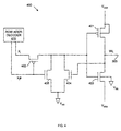
- Fig. 4 is a schematic diagram of a word line driver 400 used to drive word line 303 in accordance with one embodiment of the present invention.
- the output voltages supplied by word line driver 400 are provided to word line 303 (Fig. 3A).
- Word line driver 400 consists of P-channel transistors 401-402 and N-channel transistors 403-405.
- transistor 401 is turned on, thereby pulling word line 303 up to the positive boosted word line voltage V CCB .
- the V CCB word line voltage is high enough to turn off access transistor 301.
- pull-down transistor 403 is turned on, thereby pulling down word line 303 to the V SSB voltage.
- the generation of the V SSB word line voltage is described in more detail below.
- the gate of word line pull-up transistor 401 and the gate of word line pull-down transistor 403 are commonly connected to a pass gate formed by p-channel transistor 402.
- Transistor 402 when turned on, couples transistors 401 and 402 to receive an output signal X i provided by a row address decoder 410.
- the gate of transistor 402 is coupled to receive another output signal X j # from row address decoder 410.
- row address decoder 410 When the memory cells connected to word line 303 are selected for access, row address decoder 410 first drives the X i signal high, and then drives the X j # signal low.
- the low state of the X j # signal turns on pass transistor 402, which provides the logic high X i signal to the gates of the pull up and pull down transistors 401 and 403. Under these conditions, pull down transistor 403 is turned on, thereby coupling word line 303 to receive the V SSB word line voltage.
- row address decoder 410 controls a first subset of word lines that includes word line 303 and a plurality of other word lines. If word line 303 is not selected for access (but another word line in the first subset of word lines is selected for access), then row address decoder 410 provides logic low values for both the X i and X j # signals. Under these conditions, the gates of pull up and pull down transistors 401 and 403 are maintained at logic low states by n-channel transistor 404. Note that the gate of transistor 404 is connected to word line 303, which is maintained at a logic high value when word line 303 is not being accessed.
- transistor 404 is turned on when word line 303 is not being accessed; thereby coupling the gates of transistors 401 and 403 to the V SS supply voltage.
- the V SS supply voltage turns on pull up transistor 401 and turns off pull down transistor 403, thereby maintaining a logic high voltage (i.e., V CCB ) on word line 303.
- row address decoder 410 drives the X j # signal high, thereby turning on n-channel transistor 405.
- transistor 405 couples the gates of pull up and pull down transistors 401 and 403 to the V SS supply voltage.
- pull up transistor 401 is turned on and pull down transistor 403 is turned off.
- transistor 401 couples word line 303 to receive the V CCB voltage, thereby turning off access transistor 301 of memory cell 300.
- Pull down transistor 403 is selected to be an n-channel transistor to speed up the turn on of word line 303.
- the bulk of all n-channel transistors formed are connected to receive the V SS supply voltage.
- Fig. 3B which illustrates p-type substrate 306 coupled to receive the V SS supply voltage.
- the minimum value of the V SSB control voltage is limited to one diode voltage drop below the V SS supply voltage (i.e., one diode voltage drop below ground).
- each row of memory cells has an associated word line driver. There are usually numerous rows of memory cells (e.g., more than 100) in an embedded memory.
- the reverse junction leakage between the substrate and the sources of the n-channel pull down transistors can be quite substantial.
- the reverse junction leakage increases exponentially as the V SSB control voltage becomes more negative.
- the word line drivers are divided into groups of 32, with each group being coupled to a common V SSB coupling circuit 500.
- Fig. 5 is a block diagram illustrating a word line driver system 500 that includes a first plurality of word line drivers 400, a second plurality of V SSB coupling circuits 600, a V CCB voltage generator 700 and a V BBS voltage generator 800.
- Each V SSB coupling circuit 500 is coupled to a corresponding group of 32 word line drivers 400.
- the corresponding V SSB coupling circuit 500 is controlled to couple the V BBS voltage generator 800 to the corresponding group of 32 word line drivers.
- the V SSB coupling circuit routes the negative boosted voltage V BBS generated by the V BBS voltage generator 800 as the V SSB voltage.
- V BBS voltage generator 800 generates a V BBS voltage having a value less than one threshold voltage (V tp ) below the V SS supply voltage.
- V tp threshold voltage
- the corresponding V SSB coupling circuit 500 is controlled to couple the V SS voltage supply to the corresponding group of 32 word line drivers. That is, the V SSB coupling circuit 500 routes the V SS supply voltage as the V SSB voltage.
- the reverse junction leakage is substantially reduced. Moreover, by limiting the V BBS voltage to a voltage less than one threshold voltage below the V SS supply voltage, the reverse junction leakage is further reduced.
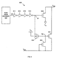
- V SSB coupling circuit 600 includes p-channel transistors 601-603, n-channel transistor 604 and inverters 611-614.
- P-channel transistor 601 is connected between the V SSB and V BBS voltage supply lines. The gate of transistor 601 is coupled to node N2.
- Transistor 602 is connected between node N2 and the V BBS voltage supply line.
- P-channel transistor 603 is connected as a capacitor, with its source and drain commonly connected to node N1, and its gate connected to node N2.
- N-channel transistor 604 is connected between the V SSB voltage supply line and the V SS voltage supply terminal.
- Inverters 611-614 are connected in series, with inverter 611 receiving the X j # signal from row address decoder 410, and inverter 614 providing the delayed X j # signal to node N1.
- Fig. 7 is a waveform diagram illustrating various signals generated during the operation of V SSB coupling circuit 600.
- the X i signal Prior to activating word line 303, the X i signal is low and the X j # signal is high. Under these conditions, the chain of inverters 611-614 provides a logic high signal to node N1, thereby turning on n-channel transistor 604. As a result, the V SSB supply line is maintained at the V SS supply voltage (0 Volts). Also, prior to activating word line 303, the sub-threshold leakage of transistor 602 pulls node N2 to a voltage less than one threshold voltage drop (V t ) above V BBS , thereby preventing transistor 601 from turning on.
- V t threshold voltage drop
- the X i signal is driven high and then the X j # signal is driven low to activate word line 303.
- pull down transistor 403 (Fig. 4) of word line driver 400 turns on, thereby coupling word line 303 to the V SSB supply line.
- the low state of the X j # is propagating through the chain of inverters 611-614 and has not reached node N1.
- n-channel transistor 604 remains on, coupling the V SSB supply line to receive the V SS supply voltage.
- the high state of node N1 pulls the source and drain of capacitor-coupled transistor 603 to a high state.
- Transistor 602 is connected as an MOS diode with its gate and drain connected to the V BBS supply line. Transistor 602 therefore limits the voltage at node N2 to no more than one threshold voltage (V t ) above the V BBS voltage, or to a potential approximately equal to the V SS supply voltage. Consequently, capacitor 603 is initially charged to a voltage approximately equal to the V dd supply voltage (i.e., the voltage across transistor 603 is approximately equal to V dd ).
- transistor 604 When the low state of the X j # signal reaches node N1, transistor 604 is turned off, thereby de-coupling the V SSB voltage supply line from the V SS voltage supply terminal.
- the low voltage at node N1 also causes capacitor 603 to pull node N2 down to a voltage equal to -V dd .
- the -V dd voltage at node N2 turns on p-channel transistor 601, thereby coupling the V SSB voltage supply line to the V BBS voltage supply line.
- Note that only 32 word line drivers are coupled to the V BBS voltage supply line (and therefore the V BBS voltage generator 800) at this time. Because a relatively small number of word line drivers are connected to the V BBS supply line, the resulting junction leakage is relatively small.
- the on-chip V BBS voltage generator 800 is designed to maintain V BBS at approximately -0.3 Volts below the V SS supply voltage despite the junction leakage. Note that during the activation of word line 303, this word line 303 is initially coupled to receive the V SS supply voltage. When the voltage of word line 303 drops below the V dd supply voltage, then word line 303 is coupled to receive the negative boosted voltage V BBS . This limits the source-to-drain voltage of word line pull down transistor 403 to be less than V CCB minus V BBS , thereby preventing transistor 403 from being exposed to high voltage stress.
- the X j # signal is driven high by row address decoder 410.
- pull up transistor 401 in word line driver 400 is turned on, thereby pulling up word line 303 to the V CCB voltage.
- V SSB coupling circuit 600 the high state of the X j # signal propagates through the delay chain formed by inverters 611-614, thereby providing a high voltage at node N1 which turns on transistor 604.
- the high voltage at node N1 also couples node N2 to a voltage of about V SS , thereby turning off transistor 601. Under these conditions, the V SSB voltage supply line is coupled to the V SS voltage supply terminal.
- V CCB and V SSB voltages are generated by on-chip charge pump circuits in accordance with one embodiment of the present invention.
- Fig. 8 is a block diagram showing the general construction of the V CCB and V SSB boosted voltage generators 700 and 800 in accordance with one embodiment of the present invention.
- Each of the V CCB and V SSB boosted voltage generators consists of a ring oscillator 801, a charge pump 802 and a pump controller 803, which controls the operation of the oscillator 801 and thus charge pump 802.
- Ring oscillator 801 and charge pump 802 are conventional elements that are well documented in references such as U.S. Patent Nos. 5,703,827 and 5,267,201.
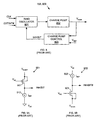
- Fig. 9A is a simplified schematic diagram of a charge pump control circuit 901 used in a conventional positive boosted voltage generator.
- Charge pump control circuit 901 includes a p-channel transistor 911 having a gate coupled to receive the V dd supply voltage, a source and bulk coupled to receive the positive boosted voltage V boost+ , and a drain coupled to a reference current source 912.
- the drain of transistor 911 is also connected to the Inhibit control line.
- Current source 912 can be replaced with a resistor.
- transistor 911 When the V boost+ voltage is higher than the V dd supply voltage by one threshold voltage (V tp ), transistor 911 is turned on. The source current from transistor 911 is compared to the reference current I REF provided by current source 912. As the potential difference between the V boost+ and V dd voltages increases, the source current from transistor 911 increases. When the source current is larger than the reference current I REF , the Inhibit control line is coupled to receive the V boost+ voltage. The high state of the Inhibit signal disables the ring oscillator 801, thereby shutting down the charge pump 802 and stopping V boost+ from going higher.
- the boosted voltage V boost+ can be regulated at a voltage equal to the V dd supply voltage plus one threshold voltage (V tp ) or higher.
- V tp threshold voltage
- the bulk of transistor 911 is coupled to receive the V boost+ voltage so that the source-to-bulk junction of this transistor is not forward biased.
- this connection is possible only when the bulk of transistor 911 is an N-well which can be isolated from the substrate, or when transistor 911 is formed in an n-type substrate that is biased to a voltage equal to or more positive than V boost+ .
- Fig. 9B is a simplified schematic diagram of a charge pump control circuit 902 used in a conventional negative boosted voltage generator.
- Charge pump control circuit 902 includes an n-channel transistor 921 having a gate coupled to receive the V SS supply voltage, a source and bulk coupled to receive the negative boosted voltage V boost- , and a drain coupled to a reference current source 922.
- the drain of transistor 921 is also connected to the Inhibit# control line.
- Current source 922 can be replaced with a resistor.
- transistor 921 When the V boost- voltage is lower than the V SS supply voltage by one threshold voltage (V tn ), transistor 921 is turned on. The drain current from transistor 921 is compared to the reference current I REF provided by current source 922. As the potential difference between V boost- and V SS increases, the drain current from transistor 921 increases. When the drain current is larger than the reference current I REF , the Inhibit# control line is coupled to receive the V boost- voltage. The low state of the Inhibit# signal disables the ring oscillator 801, thereby shutting down the charge pump 802 and stopping the V boost- voltage from going more negative.
- the V boost- voltage can be regulated at a voltage equal to V SS minus one threshold voltage (V tn ) or more.
- V tn threshold voltage
- the bulk of transistor 921 is coupled to receive the V boost- voltage so that the source-to-bulk junction of this transistor is not forward biased. This connection is possible only when the bulk of transistor 921 is a p-well which can be isolated from the substrate, or when transistor 921 is formed in a p-type substrate that is biased a voltage equal to or more negative than V boost- .
- Charge pump control circuits 901 and 902 cannot coexist in a conventional logic process because such a process has the limitation that only one type of transistor can be isolated in a well. That is, both n-wells and p-wells are not available in a conventional logic process as defined herein. Moreover, because the p-type substrate of memory cell 300 is biased at the V SS voltage (Fig. 3B), the p-type substrate of memory cell 300 cannot be biased at a voltage equal to or more negative than the negative boosted word line voltage V BBS .
- charge pump control circuit 901 results in a V boost+ voltage greater than or equal to V dd plus V tp , this charge pump control circuit 901 cannot generate a V boost+ voltage greater than the V dd supply voltage, but less than the V dd supply voltage plus the threshold voltage V tp as required by the present invention.
- charge pump control circuit 902 results in a V boost- voltage less than or equal to the V SS supply voltage minus the threshold voltage V tn , this charge pump control circuit 902 cannot generate a V boost- voltage less than the V SS supply voltage, but greater than the V SS supply voltage minus the absolute value of the threshold voltage V tn as required by the present invention.
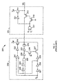
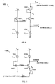
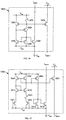
- FIG. 10 is a schematic diagram of a V CCB charge pump control circuit 1000 in accordance with the one embodiment of the present invention.
- V CCB charge pump control circuit 1000 is used to replace charge pump control circuit 803 (Fig. 8), thereby creating a V CCB reference voltage generation circuit that is capable of generating the desired V CCB voltage.
- V CCB charge pump control circuit 1000 includes p-channel transistors 1001-1003 and reference current sources 1004-1005.
- the source of p-channel transistor 1001 is coupled to receive the V dd supply voltage, and the gate and drain of p-channel transistor 1001 are commonly connected to reference current source 1004.
- P-channel transistor 1001 is thereby connected as a diode between the V dd voltage supply and reference current source 1004.
- Reference current source 1004 generates a reference current, I REFP , which establishes a reference voltage, V REFP , on the gate of p-channel transistor 1002.
- P-channel transistor 1001 has a channel width of W p .
- P-channel transistors 1001 and 1002 have the same channel lengths.
- p-channel transistor 1002 has a channel width of m times W p , where m is a multiplying constant.
- the drain of transistor 1002 is connected to another reference current source 1005, which generates a reference current, I REFP1 .
- the source of transistor 1002 is connected to node V p .
- Node V p is also connected to the drain and gate of p-channel transistor 1003.
- the source of transistor 1003 is connected to receive the positive boosted voltage V CCB from charge pump 802.
- node V p will be held at a voltage equal to the V dd supply voltage. Under these conditions, the positive boosted voltage V CCB will be higher than the V dd supply voltage by a voltage greater than the absolute value of the threshold voltage V tp of p-channel transistor 1003.
- reference current I REFP is set approximately equal to reference current I REFP1
- the multiplying constant m is set equal to four. Because the channel length of transistor 1002 is four times longer than the channel length of transistor 1001, the source-to-gate voltage of transistor 1002 is less than the source-to-gate voltage of transistor 1001. As a result, the voltage on node V p is less than the V dd supply voltage. For example, if reference currents I REFP and I REFP1 are both set equal to about 50 ⁇ A, then the voltage on node V p will be about 0.2 Volts less than the V dd supply voltage.
- the channel width of transistor 1003 is selected to be relatively large (e.g., on the order of 50 ⁇ m) such that the source-to-gate voltage of transistor 1003 is approximately equal to the threshold voltage of transistor 1003 (e.g., 0.5 Volts).
- the V CCB voltage is maintained at a voltage about 0.3 Volts greater than the V dd supply voltage.
- the V CCB voltage is therefore less than one threshold voltage greater than the V dd supply voltage.
- p-channel transistor 1003 can be eliminated, such that the V CCB voltage is provided directly to node V p .
- the channel width of transistor 1002 must be selected to smaller than the channel width W p of transistor 1001. That is, the multiplier constant m must be selected to be less than one, such that the source-to-gate voltage of transistor 1002 is greater than the source-to-gate voltage of transistor 1001 by about 0.3 Volts (or another voltage that is less than the p-channel threshold voltage).
- Fig. 11 is a schematic diagram of a V BBS charge pump control circuit 1100 in accordance with the one embodiment of the present invention.
- V BBS charge pump control circuit 1100 is used to replace charge pump control circuit 803 (Fig. 8), thereby creating a V BBS reference voltage generation circuit that is capable of generating the desired V BBS voltage.
- V BBS charge pump control circuit 1100 includes n-channel transistors 1101-1102, p-channel transistor 1103 and reference current sources 1104-1105.
- the source of n-channel transistor 1101 is connected to receive the V SS supply voltage.
- the drain and gate of transistor 1101 are commonly connected to reference current source 1104.
- transistor 1101 is connected as a diode.
- Reference current source 1104 is connected between the V dd voltage supply and the commonly connected drain and gate drain of n-channel transistor 1101. Reference current source 1104 provides a reference current I REFN1 to n-channel transistor 1101. The reference current I REFN1 establishes a reference voltage, V REFN , on the gate of n-channel transistor 1102.
- N-channel transistor 1101 has a channel width of W n .
- N-channel transistors 1101 and 1102 have the same channel lengths. However, n-channel transistor 1102 has a channel width of n times W n , where n is a multiplying constant.
- the drain of transistor 1102 is connected to another reference current source 1105, which generates a reference current, I REFN .
- the source of transistor 1102 is connected to node V N .
- Node V N is also connected to the source of p-channel transistor 1103.
- the drain and gate of transistor 1103 are commonly connected to receive the negative boosted voltage V BBS .
- V N will be held at a voltage equal to the V SS supply voltage.
- V BBS the negative boosted voltage V BBS will be regulated at a voltage approximately one threshold voltage (V tp ) below the V SS supply voltage.
- reference current I REFN is set approximately equal to reference current I REFN1
- the multiplying constant n is set equal to four. Because the channel width of transistor 1102 is four times longer than the channel width of transistor 1101, the source-to-gate voltage of transistor 1102 is less than the source-to-gate voltage of transistor 1101. As a result, the voltage potential on node V N is higher than the V SS supply voltage. For example, if reference currents I REFN and I REFN1 are both set equal to about 50 ⁇ A, then the voltage on node V N will be about 0.2 Volts greater than the V SS supply voltage.
- the channel width of transistor 1103 is selected to be relatively large (e.g., on the order of 50 ⁇ m) such that the source-to-gate voltage of transistor 1103 is approximately equal to the threshold voltage of transistor 1103 (e.g., 0.5 Volts).
- the V BBS voltage is maintained at a voltage about 0.3 Volts less than the V SS supply voltage.
- the V BBS voltage is therefore less than one threshold voltage than the V SS supply voltage.
- p-channel transistor 1103 can be eliminated, such that the V BBS voltage is provided directly to node V N .
- the channel width of transistor 1102 must be selected to smaller than the channel width W n of transistor 1101. That is, the multiplier constant n must be selected to be less than one, such that the source-to-gate voltage of transistor 1102 is greater than the source-to-gate voltage of transistor 1101 by about 0.3 Volts (or another voltage that is less than the p-channel threshold voltage).
- reference current sources 1004 and 1104 are constructed such that reference currents I REFP and I REFN1 have negative temperature coefficients (i.e., reference currents I REFP and I REFN1 decrease as the temperature increases).
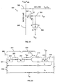
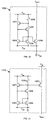
- Fig. 12 is a schematic diagram of reference current source 1004 in accordance with one embodiment of the present invention.
- Reference current source 1004 includes p-channel transistors 1201-1202, resistor 1203 and n-channel transistors 1204-1206.
- Resistor 1203 is connected between the V dd voltage supply and the gate of transistor 1201, thereby setting the bias for transistor 1201.
- the current I R through resistor 1203 is equal to the threshold voltage V tp of transistor 1201 divided by the resistance of resistor 1203.
- the current I R is therefore directly related to the threshold voltage V tp .
- the current I R flows through p-channel transistor 1202 and n-channel transistor 1205.
- the gate and source of transistor 1202 are coupled to the drain and gate, respectively, of transistor 1201.
- the voltage on the gate of transistor 1202 is translated to the drain of transistor 1202.
- N-channel transistors 1204-1206 each have a source terminal coupled to the V SS voltage supply and a gate terminal coupled to the drain of transistor 1202, thereby forming a current mirror circuit.
- the current I R is thereby translated to transistor 1206.
- the current through n-channel transistor 1206 i.e., I REFP
- I REFP the current through n-channel transistor 1206 (i.e., I REFP ) is directly related to the threshold voltage V tp of p-channel transistor 1201.
- Reference current source 1004 provides temperature compensation as follows.
- the threshold voltages V tp of transistors 1002 and 1003 decrease, thereby causing the V CCB voltage to decrease.
- the threshold voltage V tp of transistor 1201 decreases.
- the current I R decreases, thereby reducing the I REFP current.
- the gate-to-source voltage of p-channel transistor 1001 decreases, thereby increasing the V REFP voltage.
- the increased V REFP voltage causes the voltage V p to increase, thereby increasing the V CCB voltage.
- the temperature effect of the threshold voltage V tp of transistors 1002 and 1003 is thereby partially compensated by the negative temperature coefficient of the I REFP current.
- reference current source 1004 provides temperature compensation to V CCB pump control circuit 1000.
- Fig. 13 is a schematic diagram of reference current source 1104 in accordance with one embodiment of the present invention. Because reference current source 1104 is similar to reference current source 1004 (Fig. 12), similar elements in Figs. 12 and 13 are labeled with similar reference numbers. Thus, reference current source 1104 includes p-channel transistors 1201-1202, resistor 1203 and n-channel transistors 1204-1205. In addition, reference current source 1104 includes a p-channel transistor 1301 having a gate coupled to the gate of transistor 1201, and a source coupled to receive the V dd supply voltage.
- Reference current source 1104 provides temperature compensation as follows.
- the threshold voltages V t of transistors 1102 and 1103 decrease, thereby causing the V BBS voltage to increase.
- the threshold voltage V tp of p-channel transistor 1201 decreases.
- the current I R decreases.
- transistors 1201 and 1301 are coupled to form a current mirror circuit, the decrease in the current I R results in a decrease in the current I REFN1 .
- a decrease in the current I REFN1 causes a decrease in the voltage V REFN (Fig. 11).
- the decrease in V REFN results in a decrease of the voltage V N , which in turn, causes a decrease in the V BBS voltage.
- reference current source 1104 provides temperature compensation to V BBS pump control circuit 1100.
- reference current source 1004 mainly compensates for the temperature effect of transistor 1002, thereby leaving the temperature effect of transistor 1003 largely uncompensated.
- reference current source 1104 mainly compensates for the temperature effect of transistor 1102, leaving the temperature effect of transistor 1103 largely uncompensated.
- reference current sources 1005 and 1105 are constructed such that reference currents I REFP1 and I REFN have positive temperature coefficients (i.e., reference currents I REFP1 and I REFN increase as the temperature increases).
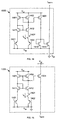
- Fig. 14 is a schematic diagram of reference current source 1005 in accordance with one embodiment of the present invention.
- Reference current source 1005 includes p-channel transistors 1401-1403, n-channel transistors 1411-1414, PNP bipolar transistors 1421-1422 and resistor 1431.
- Transistors 1401, 1411 and 1421 are connected in series between the V dd and V SS voltage supplies.
- Transistors 1402, 1412 and 1422 and resistor 1431 are connected in series between the V dd and V SS voltage supplies.
- Transistor 1403 is connected in series with parallel-connected transistors 1413-1414 between the V dd and V SS voltage supplies.
- P-channel transistors 1401-1403 are configured to form a current mirror circuit, such that the same current flows through all three of these transistors 1401-1403.
- the emitter of transistor 1422 is selected to be m times larger than the emitter of transistor 1421, where m is a multiplying constant.
- the multiplying constant m is equal to 4.
- the multiplying constant m and the resistor value of resistor 143 is selected such that the resultant current I REFP1 is approximately equal to I REFP .
- the voltages at the sources of transistors 1411 and 1412 are maintained at the same voltage by transistors 1401-1402 and 1411-1412. As a result, the voltage across transistor 1421 is equal to the voltage across resistor 1431 and transistor 1422.
- reference current source 1005 The operation of reference current source 1005 is well documented in references such as "Analysis and Design of Analog Integrated Circuits", by P.R. Gray and R.G. Meyer, pp. 330-333.
- the current I R through resistor 1431 is equal to V T /R ln(m).
- V T kT/q, where k is equal to Boltzmann's constant, T is equal to absolute temperature, and q is equal to electron charge.
- the current through resistor 1431 is therefore directly related to temperature.
- the current I R through resistor 1431 is translated to create the I REFP1 current through transistors 1403 and 1413-1414. As a result, the I REFP1 current is directly related to temperature. Thus, as temperature increases, the I REFP1 current increases.
- the increased I REFP1 current increases the gate-to-source voltages of transistors 1002 and 1003 in Fig. 10, thereby offsetting the decrease in the threshold voltage V tp of transistor 1003 which occurs with increases in temperature.
- the decrease of the threshold voltage V tp of transistor 1003 tends to decrease the V CCB voltage.
- the increased I REFP1 current tends to increase, the V CCB voltage. The net result is that the V CCB voltage is maintained relatively constant throughout the operating temperature range.
- Fig. 15 is a schematic diagram of reference current source 1105 in accordance with one embodiment of the present invention.
- Reference current source 1105 includes p-channel transistors 1401-1402 and 1501, n-channel transistors 1411-1412, PNP bipolar transistors 1421-1422 and resistor 1431.
- Transistors 1401-1402, 1411-1412, 1421-1422 and resistor 1432 are connected in the manner described above for Fig. 14.
- the gate of transistor 1501 is commonly connected to the gates of transistors 1401-1402.
- the current I R through resistor 1431 is directly related to temperature.
- the I R current through resistor 1431 increases. This increased current is translated to transistor 1501, thereby resulting in an increased I REFN current.
- the increased I REFN current increases the gate-to-source voltages of transistors 1102 and 1103 in Fig. 11, thereby offsetting the decrease in threshold voltage V tp of transistor 1103 in Fig. 11.
- the decrease in the threshold voltage V tp of transistor 1103 tends to increase the V BBS voltage.
- the increased I REFN current tends to decrease the V BBS voltage. The result is that the V BBS voltage is maintained relatively constant in the operating temperature range of the reference current circuit 1104.
- Fig. 16 is a schematic diagram illustrating reference current circuit 1600 in accordance with another embodiment of the present invention.
- Reference current circuit 1600 combines reference current circuits 1004 and 1104 in a single circuit, thereby reducing the required layout area of the resulting circuit. Similar elements in Figs. 12, 13 and 16 are labeled with similar reference numbers.
- Reference current circuit 1600 operates in the same manner as reference current circuits 1104 and 1104.
- Fig. 17 is a schematic diagram illustrating reference current circuit 1700 in accordance with another embodiment of the present invention.
- Reference current circuit 1700 combines reference current circuits 1005 and 1105 in a single circuit, thereby reducing the required layout area of the resulting circuit. Similar elements in Figs. 14, 15 and 17 are labeled with similar reference numbers.
- Reference current circuit 1700 operates in the manner as reference current circuits 1005 and 1105.
- the preferred embodiment described above uses PMOS transistors for the memory cells.
- the p-channel transistors are fabricated in N-well on P-substrate.
- the memory cells can be fabricated using NMOS transistors.
- the word line is activated high and deactivated low.
- Fig. 18 is a schematic diagram illustrating word line driver circuit 1600 and a V BBC coupling circuit 1800 that can be used to drive memory cells constructed from NMOS transistors.
- Word line driver circuit 1600 includes p-channel pull-up transistor 401 and n-channel pull-down transistor 403, which were described above in connection with word line driver 400 (Fig. 4).
- the remainder of word line driver 1600 is a reciprocal circuit of word line driver 400.
- the reciprocal circuit is obtained by replacing PMOS transistors NMOS transistors, replacing NMOS transistors with PMOS transistors, replacing connections to the V dd voltage supply with connections to the V SS voltage supply, and replacing connections to the V SS voltage supply with connections to the V dd voltage supply.
- word line driver 1600 includes n-channel transistor 1601, p-channel transistors 1602-1603 and row address decoder 1610.
- N-channel pull-down transistor 403 of word line driver 400 is coupled directly to V BBS voltage generator 800.
- the V BBS voltage generator provides a V BBS voltage about -0.3 V below the V SS supply voltage.
- the p-channel pull-up transistor 401 of word line driver 400 is coupled to receive a V BBC voltage from V BBC coupling circuit 1800.
- Row address decoder 1610 provides control signals X i # and X j , which are the inverse of the control signals X i and X j # provided by row address decoder 410 (Fig. 4).
- V BBC coupling circuit 1800 is the reciprocal the coupling circuit 600 of Fig. 6.
- V BBC coupling circuit 1800 includes n-channel transistors 1801-1803, p-channel transistor 1804 and inverters 1811-1814, as illustrated.
- the X i # signal Prior to activating word line 303, the X i # signal is high and the X j signal is low. Under these conditions, transistor 1602 is turned on, thereby applying the Vdd supply voltage to the gates of transistors 401 and 403. As a result, pull-down transistor 403 turns on, thereby providing the VBBS voltage to word line 303. Also under these conditions, the chain of inverters 1811-1814 provides a logic low signal to node N1, thereby turning on p-channel transistor 1804. As a result, the V BBC supply line is maintained at the V dd supply voltage.
- the sub-threshold leakage of transistor 1802 pulls node N2 to a voltage greater than one threshold voltage drop (V t ) below V CCB , thereby preventing transistor 1801 from turning on.
- the X i # signal is driven low and then the X j signal is driven high to activate word line 303. Under these conditions, pull up transistor 401 turns on, thereby coupling word line 303 to the V BBC voltage coupling circuit 1800. Immediately after transistor 401 is turned on, the high state of the X j signal is propagating through the chain of inverters 1811-1814 and has not reached node N1. During this time, p-channel transistor 1804 remains on, coupling the V BBC supply line to receive the V dd supply voltage. Also during this time, the low state of node N1 pulls the source and drain of capacitor-coupled transistor 1803 to a low state.
- Transistor 1802 is connected as an MOS diode with its gate and drain connected to the V CCB supply line. Transistor 1802 therefore limits the voltage at node N2 to no more than one threshold voltage (V t ) below the V CCB voltage, or to a potential approximately equal to the V dd supply voltage. Consequently, capacitor 1803 is initially charged to a voltage approximately equal to the V dd supply voltage (i.e., the voltage across transistor 1803 is approximately equal to V dd ).
- transistor 1804 When the high state of the X j signal reaches node N1, transistor 1804 is turned off, thereby de-coupling the V BBC voltage supply line from the V dd voltage supply terminal.
- the high voltage at node N1 also causes capacitor 1803 to pull node N2 up to a voltage equal to 2V dd .
- the 2V dd voltage at node N2 turns on n-channel transistor 1801, thereby coupling the V CCB voltage supply line to the V BBC voltage supply line.
Landscapes
- Engineering & Computer Science (AREA)
- Microelectronics & Electronic Packaging (AREA)
- Computer Hardware Design (AREA)
- Power Engineering (AREA)
- Dram (AREA)
- Semiconductor Integrated Circuits (AREA)
- Semiconductor Memories (AREA)
Abstract
Claims (30)
- Système de mémoire qui fonctionne en réponse à une tension d'alimentation positive et à une tension d'alimentation de terre, le système de mémoire comprenant :où la ligne de mots (303) est activée pour accéder à la cellule DRAM (300); un excitateur de ligne de mots (400) couplé à la ligne de mots (303); et un générateur de tension survoltée positive (700) étant couplé à l'excitateur de ligne de mots (400), pour fournir une tension d'alimentation positive, caractérisé en ce que la tension survoltée positive est plus élevée que la tension d'alimentation positive (Vdd) et plus basse qu'une tension seuil de transistor (Vt) plus élevée que la tension d'alimentation positive (Vdd).une cellule de mémoire vive dynamique (DRAM) (300);une ligne de mots (303) couplée à la cellule DRAM (300) .
- Le système de mémoire de la revendication 1, dans lequel l'excitateur de ligne de mots (400) comprend un transistor à canal p (301) couplé entre la ligne de mots (303) et le générateur de tension survoltée positive (700), et un transistor à canal n couplé à la ligne de mots (303).
- Le système de mémoire de la revendication 2, comprenant en outre un générateur de tension survoltée négative (800) pour fournir une tension survoltée négative plus basse que la tension d'alimentation de terre (Vss), le générateur de tension survoltée négative (800) étant couplé à l'excitateur de ligne de mots (400).
- Le système de mémoire de la revendication 3, dans lequel la tension survoltée négative est plus basse que la tension d'alimentation de terre (Vss) d'une tension moindre que la valeur absolue d'une tension seuil de transistor (Vt).
- Le système de mémoire de la revendication 4, dans lequel la cellule DRAM (300) comprend :un premier transistor à canal p (301) ayant une grille couplée à la ligne de mots (303); etun deuxième dispositif à canal p (302) couplé au premier transistor à canal p (301), le deuxième dispositif à canal p (302) étant configuré comme un condensateur de stockage.
- Le système de mémoire de la revendication 1, dans lequel le système de mémoire est fabriqué en utilisant un processus logique conventionnel.
- Le système de mémoire de la revendication 3, comprenant en outre un circuit de couplage (500; 600) couplé entre l'excitateur de ligne de mots (400) et le générateur de tension survoltée négative (800), le circuit de couplage (500; 600) étant configuré pour fournir la tension d'alimentation de terre (Vss) à l'excitateur de ligne de mots (400) lorsque la ligne de mots (303) est activée pour la première fois, le circuit de couplage (500; 600) étant configuré en plus pour fournir la tension survoltée négative à l'excitateur de ligne de mots (400) lorsque la tension sur la ligne de mots (303) tombe au-dessous de la tension d'alimentation positive (Vdd).
- Le système de mémoire de la revendication 7, dans lequel le circuit de couplage (500; 600) comprend :un premier transistor (601) couplé entre l'excitateur de ligne de mots (400) et une borne fournissant la tension d'alimentation de terre (Vss);un deuxième transistor (602) couplé entre l'excitateur de ligne de mots et le générateur de tension survoltée négative (800); etune chaíne de retard couplée à une grille du premier transistor (601).
- Le système de mémoire de la revendication 8, comprenant en outre :un condensateur couplé entre la chaíne de retard et une grille du deuxième transistor; etun élément à diode couplé entre la grille du deuxième transistor et le générateur de tension survoltée négative .
- Le système de mémoire de la revendication 3, comprenant en outre un circuit de couplage (500; 600) couplé entre le transistor à canal n (604) et le générateur de tension survoltée négative (800), le circuit de couplage (500; 600) étant configuré pour coupler le générateur de tension survoltée négative (800) au transistor à canal n (604) lorsque la ligne de mots (303) est activée, et le circuit de couplage (500; 600) étant configuré pour fournir la tension d'alimentation de terre (Vss) au transistor à canal n (604) lorsque la ligne de mots (303) n'est pas activée.
- Système de mémoire qui fonctionne en réponse à une tension d'alimentation positive et à une tension d'alimentation de terre, le système de mémoire comprenant :où la ligne de mots (303) est activée pour accéder à la cellule DRAM (300), un excitateur de ligne de mots (400) couplé à la ligne de mots (303); et un générateur de tension survoltée négative (800) qui est couplé à l'excitateur de ligne de mots, pour fournir une tension survoltée négative, caractérisé en ce que la tension survoltée . négative est plus basse que la tension d'alimentation de terre (Vss) d'une tension moindre que la valeur absolue d'une tension seuil de transistor (Vt).une cellule de mémoire vive dynamique (DRAM) (300);une ligne de mots (303) couplée à la cellule DRAM (300),
- Le système de mémoire de la revendication 11, dans lequel l'excitateur de ligne de mots (400) comprend un transistor à canal n (604) couplé entre la ligne de mots (303) et le générateur de tension survoltée négative (800), et un transistor à canal p (600) couplé à la ligne de mots (303).
- Le système de mémoire de la revendication 12, comprenant en outre un générateur de tension survoltée positive (700) pour fournir une tension survoltée positive plus élevée que la tension positive d'alimentation, le générateur de tension survoltée positive (700) étant couplé à l'excitateur de ligne de mots (400).
- Le système de mémoire de la revendication 13, dans lequel la tension survoltée positive est plus élevée que la tension d'alimentation positive de moins d'une tension seuil de transistor (Vt).
- Le système de mémoire de la revendication 13, comprenant en outre un circuit de couplage (500; 600) entre le transistor à canal p (601) et le générateur de tension survoltée positive (700), le circuit de couplage (500; 600) étant configuré pour coupler le générateur de tension survoltée positive (700) au transistor à canal p (601) lorsque la ligne de mots (302) est activée, et le circuit de couplage (500; 600) étant configuré pour fournir la tension d'alimentation positive au transistor à canal p (601) lorsque la ligne de mots (303) n'est pas activée.
- Le système de mémoire de la revendication 15, dans lequel la cellule DRAM (300) comprend :un premier transistor à canal n ayant une grille couplée à la ligne de mots; etun deuxième dispositif à canal n couplé au premier transistor à canal n, le deuxième dispositif à canal n étant configuré comme un condensateur de stockage.
- Le système de mémoire de la revendication 11, dans lequel le système de mémoire est fabriqué en utilisant un processus logique conventionnel.
- Le système de mémoire de la revendication 13, comprenant en outre un circuit de couplage (500; 600) couplé entre l'excitateur de ligne de mots et le générateur de tension survoltée positive (700), le circuit de couplage étant configuré pour fournir la tension d'alimentation positive à l'excitateur de ligne de mots (400) lorsque la ligne de mots est activée pour la première fois, le circuit de couplage étant configuré en plus pour fournir la tension survoltée positive à l'excitateur de ligne de mots (400) lorsque la tension sur la ligne de mots (303) s'élève au-dessus de la tension d'alimentation de terrre.
- Le système de mémoire de la revendication 18, dans lequel le circuit de couplage comprend :un premier transistor couplé entre l'excitateur de ligne de mots et une borne fournissant la tension d'alimentation positive;un deuxième transistor couplé entre l'excitateur de ligne de mots et le générateur de tension survoltée positive; etune chaíne de retard couplée à une grille du premier transistor.
- Le système de mémoire de la revendication 19, comprenant en outre :un condensateur couplé entre la chaíne de retard et une grille du deuxième transistor; etun élément à diode couplé entre la grille du deuxième transistor et le générateur de tension survoltée positive.
- Méthode pour exciter une ligne de mots couplée à une cellule de mémoire vive dynamique (DRAM) (300), la méthode comprenant les étapes consistant à :générer une tension survoltée négative fournissant latension d'alimentation de terre à la ligne de mots (303) lorsque la ligne de mots (303) est activée pour la première fois; et puis fournir latension survoltée négative à la ligne de mots (303) lorsque la tension sur la ligne de mots (303) tombe au-dessous d'une tension d'alimentation positive; caractérisée en ce que la tension survoltée négative est plus basse qu'une tension d'alimentation de terre de moins d'une tension seuil de transistor.
- La méthode de la revendication 21, comprenant en outre les étapes consistant à :générer une tension survoltée positive plus élevée qu'une tension d'alimentation positive de moins d'une tension seuil de transistor; etexciter la ligne de mots (303) avec la tension survoltée positive lorsque la cellule DRAM (300) n'est pas accédée.
- Méthode pour exciter une ligne de mots (303) couplée à une cellule de mémoire vive dynamique (DRAM) (303), la méthode comprenant les étapes consistant à :générer une tension survoltée positive plus élevée qu'une tension d'alimentation positive de moins d'une tension seuil de transistor;fournir la tension d'alimentation positive à la ligne de mots (303) lorsque la tension sur la ligne de mots (303) est activée pour la première fois; et puisfournir la tension survoltée positive à la ligne de mots (303) lorsque la tension sur la ligne de mots (303) s'élève au-dessus de la tension d'alimentation de terre.
- La méthode de la revendication 23, comprenant en outre les étapes consistant à :générer une tension survoltée négative plus basse qu'une tension d'alimentation de terre de moins d'une tension seuil de transistor; etexciter la ligne de mots (303) avec la tension survoltée négative lorsque la cellule DRAM (300) n'est pas accédée.
- Circuit de contrôle de pompe de charge (901; 1000) pour générer un circuit de contrôle de pompe de charge de tension survoltée positive (901; 1000) comprenant :un premier transistor à canal p (911) ayant une source couplée à la tension d'alimentation positive, le premier transistor à canal p (911) ayant une première largeur de canal;une première source de courant de référence (912) couplée à un drain du premier transistor à canal p (911);un deuxième transistor à canal p ayant une grille couplée à une grille du premier transistor à canal p, le deuxième transistor à canal p ayant une deuxième largeur de canal, où la deuxième largeur de canal est plus grande que la première largeur de canal;une deuxième source de courant de référence couplée à un drain du deuxième transistor à canal p; etun troisième transistor à canal p ayant une grille et un drain connectés à une source du deuxième transistor à canal p, le troisième transistor à canal p ayant en plus une source couplée pour recevoir la tension survoltée positive, caractérisé en ce que la tension survoltée positive est plus élevée qu'une tension d'alimentation positive de moins d'une tension seuil.
- Le circuit de contrôle de pompe de charge de la revendication 25, dans lequel la première source de courant de référence a un coefficient de température négatif.
- Le circuit de contrôle de pompe de charge de la revendication 25, dans lequel la deuxième source de courant de référence a un coefficient de température positif.
- Circuit de contrôle de pompe de charge (902; 1100) pour générer une tension survoltée négative, le circuit de contrôle de pompe de charge comprenant :caractérisé en ce que la tension survoltée négative est plus basse qu'une tension d'alimentation de terre de moins d'une tension seuil de transistor.un premier transistor à canal n (921) ayant une source couplée à la tension d'alimentation de terre (Vss), le premier transistor à canal n ayant une première largeur de canal;une première source de courant de référence couplée à un drain du premier transistor à canal n;un deuxième transistor à canal n ayant une grille couplée à une grille du premier transistor à canal n, le deuxième transistor à canal n ayant une deuxième largeur de canal, où la deuxième largeur de canal est plus grande que la première largeur de canal;une deuxième source de courant de référence couplée à un drain du deuxième transistor à canal n; etun transistor à canal p ayant une source connectée à une source du deuxième transistor à canal n, le transistor à canal p ayant en plus une grille et un drain couplés pour recevoir la tension survoltée négative .
- Le circuit de contrôle de pompe de charge de la revendication 28, dans lequel la première source de courant de référence a un coefficient de température négatif.
- Le circuit de contrôle de pompe de charge de la revendication 29, dans lequel la deuxième source de courant de référence a un coefficient de température positif.
Applications Claiming Priority (5)
| Application Number | Priority Date | Filing Date | Title |
|---|---|---|---|
| US09/134,488 US6075720A (en) | 1998-08-14 | 1998-08-14 | Memory cell for DRAM embedded in logic |
| US134488 | 1998-08-14 | ||
| US332757 | 1999-06-14 | ||
| US09/332,757 US6147914A (en) | 1998-08-14 | 1999-06-14 | On-chip word line voltage generation for DRAM embedded in logic process |
| PCT/US1999/018536 WO2000010171A1 (fr) | 1998-08-14 | 1999-08-13 | Generation de tension de canal mot sur puce pour memoire vive dynamique incorporee a un procede logique |
Publications (2)
| Publication Number | Publication Date |
|---|---|
| EP1105875A1 EP1105875A1 (fr) | 2001-06-13 |
| EP1105875B1 true EP1105875B1 (fr) | 2002-11-06 |
Family
ID=26832381
Family Applications (1)
| Application Number | Title | Priority Date | Filing Date |
|---|---|---|---|
| EP99942197A Expired - Lifetime EP1105875B1 (fr) | 1998-08-14 | 1999-08-13 | Generation de tension de canal mot sur puce pour memoire vive dynamique incorporee a un procede logique |
Country Status (5)
| Country | Link |
|---|---|
| US (1) | US6147914A (fr) |
| EP (1) | EP1105875B1 (fr) |
| JP (1) | JP2002522871A (fr) |
| DE (1) | DE69903835T2 (fr) |
| WO (1) | WO2000010171A1 (fr) |
Families Citing this family (35)
| Publication number | Priority date | Publication date | Assignee | Title |
|---|---|---|---|---|
| US6468855B2 (en) * | 1998-08-14 | 2002-10-22 | Monolithic System Technology, Inc. | Reduced topography DRAM cell fabricated using a modified logic process and method for operating same |
| US6297686B1 (en) * | 1999-05-28 | 2001-10-02 | Winbond Electronics Corporation | Semiconductor integrated circuit for low-voltage high-speed operation |
| US6841821B2 (en) * | 1999-10-07 | 2005-01-11 | Monolithic System Technology, Inc. | Non-volatile memory cell fabricated with slight modification to a conventional logic process and methods of operating same |
| US6329240B1 (en) * | 1999-10-07 | 2001-12-11 | Monolithic System Technology, Inc. | Non-volatile memory cell and methods of fabricating and operating same |
| KR100362700B1 (ko) * | 2000-02-03 | 2002-11-27 | 삼성전자 주식회사 | 반도체 메모리 장치의 전압 레귤레이터 회로 |
| US6381182B1 (en) * | 2000-09-13 | 2002-04-30 | Infineon Technologies Ag | Combined tracking of WLL and VPP low threshold voltage in DRAM array |
| US6515917B2 (en) * | 2001-04-10 | 2003-02-04 | International Business Machines Corporation | Digital-to-analog converter (dac) for dynamic adjustment of off-chip driver pull-up and pull down impedance by providing a variable reference voltage to high frequency receiver and driver circuits for commercial memory |
| US7336121B2 (en) * | 2001-05-04 | 2008-02-26 | Samsung Electronics Co., Ltd. | Negative voltage generator for a semiconductor memory device |
| US20030197546A1 (en) * | 2001-07-09 | 2003-10-23 | Samsung Electronics Co., Ltd. | Negative voltage generator for a semiconductor memory device |
| US6751152B2 (en) * | 2001-10-31 | 2004-06-15 | International Business Machines Corporation | Method and configuration to allow a lower wordline boosted voltage operation while increasing a sensing signal with access transistor threshold voltage |
| KR100609193B1 (ko) | 2002-02-14 | 2006-08-02 | 마츠시타 덴끼 산교 가부시키가이샤 | 반도체장치 및 그 제조방법 |
| JP3816022B2 (ja) | 2002-05-28 | 2006-08-30 | 松下電器産業株式会社 | 半導体記憶装置 |
| JP2004213722A (ja) | 2002-12-27 | 2004-07-29 | Matsushita Electric Ind Co Ltd | 半導体記憶装置及び半導体集積回路装置 |
| KR100542708B1 (ko) * | 2003-05-28 | 2006-01-11 | 주식회사 하이닉스반도체 | 고전압 발생기 |
| KR100610005B1 (ko) * | 2003-08-25 | 2006-08-09 | 삼성전자주식회사 | 반도체 메모리 소자의 네거티브 전압 발생장치 및네거티브 전압 생성제어방법 |
| US6930536B2 (en) * | 2003-11-04 | 2005-08-16 | Micron Technology, Inc. | Voltage booster |
| JP2005222659A (ja) * | 2004-02-09 | 2005-08-18 | Matsushita Electric Ind Co Ltd | 半導体記憶装置 |
| US7142043B2 (en) * | 2004-08-02 | 2006-11-28 | Taiwan Semiconductor Manufacturing Co., Ltd. | On chip word line voltage with PVT tracking for memory embedded in logic process |
| JP4962828B2 (ja) * | 2004-08-25 | 2012-06-27 | マイクロン テクノロジー, インク. | ワード線ドライバ回路およびこれを利用する方法 |
| US7068024B1 (en) * | 2004-12-30 | 2006-06-27 | Taiwan Semiconductor Manufacturing Company, Ltd. | Voltage regulator having positive temperature coefficient for self-compensation and related method of regulating voltage |
| US7323379B2 (en) * | 2005-02-03 | 2008-01-29 | Mosys, Inc. | Fabrication process for increased capacitance in an embedded DRAM memory |
| US7855932B2 (en) | 2005-03-04 | 2010-12-21 | Taiwan Semiconductor Manufacturing Co., Ltd. | Low power word line control circuits with boosted voltage output for semiconductor memory |
| US7274618B2 (en) * | 2005-06-24 | 2007-09-25 | Monolithic System Technology, Inc. | Word line driver for DRAM embedded in a logic process |
| US7499307B2 (en) * | 2005-06-24 | 2009-03-03 | Mosys, Inc. | Scalable embedded DRAM array |
| JP2007059024A (ja) * | 2005-08-26 | 2007-03-08 | Micron Technol Inc | 温度補償された読み出し・検証動作をフラッシュ・メモリにおいて生成するための方法及び装置 |
| JP2007058772A (ja) * | 2005-08-26 | 2007-03-08 | Micron Technol Inc | バンド・ギャップ基準から可変出力電圧を生成する方法及び装置 |
| JP2007060544A (ja) * | 2005-08-26 | 2007-03-08 | Micron Technol Inc | 温度係数が小さいパワー・オン・リセットを生成する方法及び装置 |
| CN100414838C (zh) * | 2005-12-20 | 2008-08-27 | 北京芯技佳易微电子科技有限公司 | 标准逻辑工艺上的负电压有效传输电路 |
| US8648403B2 (en) | 2006-04-21 | 2014-02-11 | International Business Machines Corporation | Dynamic memory cell structures |
| US7489556B2 (en) * | 2006-05-12 | 2009-02-10 | Micron Technology, Inc. | Method and apparatus for generating read and verify operations in non-volatile memories |
| JP4951786B2 (ja) * | 2007-05-10 | 2012-06-13 | ルネサスエレクトロニクス株式会社 | 半導体記憶装置 |
| US7929359B2 (en) * | 2008-11-13 | 2011-04-19 | Mosys, Inc. | Embedded DRAM with bias-independent capacitance |
| JP5202248B2 (ja) * | 2008-11-26 | 2013-06-05 | パナソニック株式会社 | 半導体記憶装置 |
| TWI525614B (zh) * | 2011-01-05 | 2016-03-11 | 半導體能源研究所股份有限公司 | 儲存元件、儲存裝置、及信號處理電路 |
| US9209167B2 (en) * | 2014-03-25 | 2015-12-08 | International Business Machines Corporation | Determining threshold voltage variations in field effect transistors |
Family Cites Families (9)
| Publication number | Priority date | Publication date | Assignee | Title |
|---|---|---|---|---|
| JPH0442494A (ja) * | 1990-06-08 | 1992-02-13 | Nec Corp | Mosダイナミックram |
| US5075571A (en) * | 1991-01-02 | 1991-12-24 | International Business Machines Corp. | PMOS wordline boost cricuit for DRAM |
| KR940002859B1 (ko) * | 1991-03-14 | 1994-04-04 | 삼성전자 주식회사 | 반도체 메모리장치에서의 워드라인 구동회로 |
| JP2905666B2 (ja) * | 1992-05-25 | 1999-06-14 | 三菱電機株式会社 | 半導体装置における内部電圧発生回路および不揮発性半導体記憶装置 |
| JP2731701B2 (ja) * | 1993-06-30 | 1998-03-25 | インターナショナル・ビジネス・マシーンズ・コーポレイション | Dramセル |
| JPH0863964A (ja) * | 1994-08-29 | 1996-03-08 | Mitsubishi Electric Corp | 半導体記憶装置 |
| US5703827A (en) * | 1996-02-29 | 1997-12-30 | Monolithic System Technology, Inc. | Method and structure for generating a boosted word line voltage and a back bias voltage for a memory array |
| KR100257866B1 (ko) * | 1997-04-11 | 2000-06-01 | 윤종용 | 챠아지 펌핑 회로를 가지는 불 휘발성 메모리 장치 |
| US6009023A (en) * | 1998-05-26 | 1999-12-28 | Etron Technology, Inc. | High performance DRAM structure employing multiple thickness gate oxide |
-
1999
- 1999-06-14 US US09/332,757 patent/US6147914A/en not_active Expired - Lifetime
- 1999-08-13 JP JP2000565540A patent/JP2002522871A/ja active Pending
- 1999-08-13 EP EP99942197A patent/EP1105875B1/fr not_active Expired - Lifetime
- 1999-08-13 WO PCT/US1999/018536 patent/WO2000010171A1/fr not_active Ceased
- 1999-08-13 DE DE69903835T patent/DE69903835T2/de not_active Expired - Lifetime
Also Published As
| Publication number | Publication date |
|---|---|
| DE69903835T2 (de) | 2003-02-27 |
| US6147914A (en) | 2000-11-14 |
| JP2002522871A (ja) | 2002-07-23 |
| WO2000010171A1 (fr) | 2000-02-24 |
| EP1105875A1 (fr) | 2001-06-13 |
| DE69903835D1 (de) | 2002-12-12 |
Similar Documents
| Publication | Publication Date | Title |
|---|---|---|
| US6147914A (en) | On-chip word line voltage generation for DRAM embedded in logic process | |
| US6784048B2 (en) | Method of fabricating a DRAM cell having a thin dielectric access transistor and a thick dielectric storage | |
| US7447104B2 (en) | Word line driver for DRAM embedded in a logic process | |
| JP4316884B2 (ja) | キャビティ内に部分的に製造されたコンデンサ構造を備えたdramセル及びその製造方法 | |
| US6545525B2 (en) | Semiconductor device including interface circuit, logic circuit, and static memory array having transistors of various threshold voltages and being supplied with various supply voltages | |
| JP3085455B2 (ja) | スタティックram | |
| US6175138B1 (en) | Semiconductor memory device and method of manufacturing the same | |
| US5255224A (en) | Boosted drive system for master/local word line memory architecture | |
| US6075720A (en) | Memory cell for DRAM embedded in logic | |
| GB2269049A (en) | Semiconductor memory device | |
| US20020110017A1 (en) | Voltage generator for semiconductor device | |
| US6509595B1 (en) | DRAM cell fabricated using a modified logic process and method for operating same | |
| JP3853088B2 (ja) | 半導体メモリ装置の内部電源電圧発生回路及びその制御方法 | |
| JP2004213722A (ja) | 半導体記憶装置及び半導体集積回路装置 | |
| US5825703A (en) | Semiconductor memory device having p-channel field effect transistor to drive word line |
Legal Events
| Date | Code | Title | Description |
|---|---|---|---|
| PUAI | Public reference made under article 153(3) epc to a published international application that has entered the european phase |
Free format text: ORIGINAL CODE: 0009012 |
|
| 17P | Request for examination filed |
Effective date: 20010202 |
|
| AK | Designated contracting states |
Kind code of ref document: A1 Designated state(s): AT BE CH CY DE DK ES FI FR GB GR IE IT LI LU MC NL PT SE |
|
| 17Q | First examination report despatched |
Effective date: 20010615 |
|
| GRAG | Despatch of communication of intention to grant |
Free format text: ORIGINAL CODE: EPIDOS AGRA |
|
| GRAG | Despatch of communication of intention to grant |
Free format text: ORIGINAL CODE: EPIDOS AGRA |
|
| GRAH | Despatch of communication of intention to grant a patent |
Free format text: ORIGINAL CODE: EPIDOS IGRA |
|
| GRAH | Despatch of communication of intention to grant a patent |
Free format text: ORIGINAL CODE: EPIDOS IGRA |
|
| GRAA | (expected) grant |
Free format text: ORIGINAL CODE: 0009210 |
|
| AK | Designated contracting states |
Kind code of ref document: B1 Designated state(s): DE FR GB |
|
| REG | Reference to a national code |
Ref country code: GB Ref legal event code: FG4D |
|
| REG | Reference to a national code |
Ref country code: IE Ref legal event code: FG4D |
|
| REF | Corresponds to: |
Ref document number: 69903835 Country of ref document: DE Date of ref document: 20021212 |
|
| ET | Fr: translation filed | ||
| PLBE | No opposition filed within time limit |
Free format text: ORIGINAL CODE: 0009261 |
|
| STAA | Information on the status of an ep patent application or granted ep patent |
Free format text: STATUS: NO OPPOSITION FILED WITHIN TIME LIMIT |
|
| 26N | No opposition filed |
Effective date: 20030807 |
|
| REG | Reference to a national code |
Ref country code: IE Ref legal event code: MM4A |
|
| REG | Reference to a national code |
Ref country code: DE Ref legal event code: R082 Ref document number: 69903835 Country of ref document: DE Representative=s name: WILHELMS, KILIAN & PARTNER, DE Ref country code: DE Ref legal event code: R082 Ref document number: 69903835 Country of ref document: DE Representative=s name: BOSCH JEHLE PATENTANWALTSGESELLSCHAFT MBH, DE |
|
| REG | Reference to a national code |
Ref country code: DE Ref legal event code: R082 Ref document number: 69903835 Country of ref document: DE Representative=s name: BOSCH JEHLE PATENTANWALTSGESELLSCHAFT MBH, DE |
|
| REG | Reference to a national code |
Ref country code: GB Ref legal event code: 732E Free format text: REGISTERED BETWEEN 20120705 AND 20120711 |
|
| REG | Reference to a national code |
Ref country code: DE Ref legal event code: R082 Ref document number: 69903835 Country of ref document: DE Representative=s name: BOSCH JEHLE PATENTANWALTSGESELLSCHAFT MBH, DE Effective date: 20120124 Ref country code: DE Ref legal event code: R082 Ref document number: 69903835 Country of ref document: DE Representative=s name: BOSCH JEHLE PATENTANWALTSGESELLSCHAFT MBH, DE Effective date: 20120611 Ref country code: DE Ref legal event code: R081 Ref document number: 69903835 Country of ref document: DE Owner name: INVENSAS CORP., SAN JOSE, US Free format text: FORMER OWNER: MONOLITHIC SYSTEM TECHNOLOGY, INC., SUNNYVALE, CALIF., US Effective date: 20120611 |
|
| REG | Reference to a national code |
Ref country code: FR Ref legal event code: TP Owner name: INVENSAS CORPORATION, US Effective date: 20120720 Ref country code: FR Ref legal event code: CD Owner name: INVENSAS CORPORATION, US Effective date: 20120720 |
|
| REG | Reference to a national code |
Ref country code: FR Ref legal event code: PLFP Year of fee payment: 17 |
|
| REG | Reference to a national code |
Ref country code: FR Ref legal event code: PLFP Year of fee payment: 18 |
|
| REG | Reference to a national code |
Ref country code: FR Ref legal event code: PLFP Year of fee payment: 19 |
|
| REG | Reference to a national code |
Ref country code: FR Ref legal event code: PLFP Year of fee payment: 20 |
|
| PGFP | Annual fee paid to national office [announced via postgrant information from national office to epo] |
Ref country code: FR Payment date: 20180827 Year of fee payment: 20 Ref country code: DE Payment date: 20180829 Year of fee payment: 20 |
|
| PGFP | Annual fee paid to national office [announced via postgrant information from national office to epo] |
Ref country code: GB Payment date: 20180828 Year of fee payment: 20 |
|
| REG | Reference to a national code |
Ref country code: DE Ref legal event code: R071 Ref document number: 69903835 Country of ref document: DE |
|
| REG | Reference to a national code |
Ref country code: GB Ref legal event code: PE20 Expiry date: 20190812 |
|
| PG25 | Lapsed in a contracting state [announced via postgrant information from national office to epo] |
Ref country code: GB Free format text: LAPSE BECAUSE OF EXPIRATION OF PROTECTION Effective date: 20190812 |