EP1107308A1 - Procédé pour la fabrication d'une interconnexion à plusieurs niveaux pour un circuit intégré utilisant une couche protectrice - Google Patents
Procédé pour la fabrication d'une interconnexion à plusieurs niveaux pour un circuit intégré utilisant une couche protectrice Download PDFInfo
- Publication number
- EP1107308A1 EP1107308A1 EP00310512A EP00310512A EP1107308A1 EP 1107308 A1 EP1107308 A1 EP 1107308A1 EP 00310512 A EP00310512 A EP 00310512A EP 00310512 A EP00310512 A EP 00310512A EP 1107308 A1 EP1107308 A1 EP 1107308A1
- Authority
- EP
- European Patent Office
- Prior art keywords
- dielectric layer
- layer
- selective overlayer
- opening
- etching
- Prior art date
- Legal status (The legal status is an assumption and is not a legal conclusion. Google has not performed a legal analysis and makes no representation as to the accuracy of the status listed.)
- Withdrawn
Links
Images




Classifications
-
- H—ELECTRICITY
- H10—SEMICONDUCTOR DEVICES; ELECTRIC SOLID-STATE DEVICES NOT OTHERWISE PROVIDED FOR
- H10P—GENERIC PROCESSES OR APPARATUS FOR THE MANUFACTURE OR TREATMENT OF DEVICES COVERED BY CLASS H10
- H10P14/00—Formation of materials, e.g. in the shape of layers or pillars
- H10P14/40—Formation of materials, e.g. in the shape of layers or pillars of conductive or resistive materials
-
- H—ELECTRICITY
- H10—SEMICONDUCTOR DEVICES; ELECTRIC SOLID-STATE DEVICES NOT OTHERWISE PROVIDED FOR
- H10W—GENERIC PACKAGES, INTERCONNECTIONS, CONNECTORS OR OTHER CONSTRUCTIONAL DETAILS OF DEVICES COVERED BY CLASS H10
- H10W20/00—Interconnections in chips, wafers or substrates
- H10W20/01—Manufacture or treatment
- H10W20/071—Manufacture or treatment of dielectric parts thereof
- H10W20/081—Manufacture or treatment of dielectric parts thereof by forming openings in the dielectric parts
- H10W20/084—Manufacture or treatment of dielectric parts thereof by forming openings in the dielectric parts for dual-damascene structures
-
- H—ELECTRICITY
- H10—SEMICONDUCTOR DEVICES; ELECTRIC SOLID-STATE DEVICES NOT OTHERWISE PROVIDED FOR
- H10W—GENERIC PACKAGES, INTERCONNECTIONS, CONNECTORS OR OTHER CONSTRUCTIONAL DETAILS OF DEVICES COVERED BY CLASS H10
- H10W20/00—Interconnections in chips, wafers or substrates
- H10W20/01—Manufacture or treatment
- H10W20/071—Manufacture or treatment of dielectric parts thereof
- H10W20/081—Manufacture or treatment of dielectric parts thereof by forming openings in the dielectric parts
- H10W20/084—Manufacture or treatment of dielectric parts thereof by forming openings in the dielectric parts for dual-damascene structures
- H10W20/088—Manufacture or treatment of dielectric parts thereof by forming openings in the dielectric parts for dual-damascene structures involving partial etching of via holes
-
- B—PERFORMING OPERATIONS; TRANSPORTING
- B82—NANOTECHNOLOGY
- B82Y—SPECIFIC USES OR APPLICATIONS OF NANOSTRUCTURES; MEASUREMENT OR ANALYSIS OF NANOSTRUCTURES; MANUFACTURE OR TREATMENT OF NANOSTRUCTURES
- B82Y40/00—Manufacture or treatment of nanostructures
Definitions
- the present invention relates to methods for fabricating a multi-level interconnection for an integrated circuit device, and more specifically, to methods for making a dual damascene contact.
- Damascene processing is a fabrication technique that involves the creation of interconnect lines by first etching a trench in a planar dielectric layer, and then filling that trench with a conductor. This is the preferred method for fabricating semiconductor devices with copper metal interconnects because copper is not easily patterned using conventional anisotropic etching techniques.
- Dual damascene is a multilevel interconnection process in which the filling of the trench and the contact or via openings, which form the connections to the previous interconnect level with metal, is done simultaneously.
- FIGs. 1A-1D are cross-section views showing steps of a conventional full-via first dual damascene fabrication method.
- a semiconductor substrate 100 is provided having semiconductor devices 110 formed therein.
- a composite dielectric layer is then formed over the semiconductor substrate, wherein the composite dielectric layer comprises a barrier dielectric layer 120 of a first dielectric material, a via dielectric layer 130 of a second dielectric material, an etch stop dielectric layer 140 of a third dielectric material, and a trench dielectric layer 150 of a fourth dielectric material.
- a first patterned photoresist layer 160 is formed over the composite layer exposing a via opening 170 .
- the via opening 170 is transferred through the trench dielectric layer 150 , etch stop dielectric layer 140 , and via dielectric layer 130 exposing the barrier dielectric layer 120 .
- the first patterned photoresist layer is removed and a second patterned photoresist layer 180 is formed over the composite layer to define a trench opening 190 .
- the trench opening 190 is transferred through the trench dielectric layer 150 , whereby the etch stop dielectric layer 140 prevents erosion of the via dielectric layer 130 .
- the trench opening 190 is then transferred through the etch stop dielectric layer 140 exposing the via dielectric layer 130
- the via opening 170 is transferred through the barrier dielectric layer 120 exposing a conductor 110 within the semiconductor substrate 100 .
- a conductive layer (not shown) can then be formed over the entire structure, filling both the via and trench openings 170 , 190 . Thereafter, a polishing process can be performed to planarize the dual damascene structure.
- the full-via first method is problematic because, for example, the initial via is relatively deep, has a high aspect ratio, and typically requires etching through three dielectric layers (e.g., the trench dielectric, etch stop dielectric, and via dielectric). Forming this deep via can be very slow and requires the etch process to have a high degree of profile control and excellent selectivity to the first patterned photoresist layer in order to provide suitable results.
- selectivity is the etch rate of one dielectric material divided by the etch rate of a second dielectric material wherein a high degree of selectivity implies that the first dielectric etches much slower than the second dielectric. If the selectivity between the first patterned photoresist layer and the dielectric layers is not sufficiently high, the etching process will remove the first patterned photoresist layer and begin eroding the trench dielectric before the via is fully formed.
- FIGs. 2A-2D are cross-sectional views illustrating steps of a conventional partial-via first fabrication method wherein the structural layers are substantially the same as those described above in connection with the full-via first method.
- a first patterned photoresist layer 160 is formed over the trench dielectric layer 150 to define a via opening 170 .
- the via opening 170 is transferred through the trench dielectric layer 150 and the etch stop dielectric layer 140 but, unlike the full-via first method, the via opening 170 is only partially transferred into the via dielectric layer 130 .
- the first patterned photoresist layer is then removed and a second patterned photoresist layer 180 is formed to define a trench opening 190 . Referring to FIG.
- the via opening 170 is then transferred through the via dielectric layer 130 exposing the barrier dielectric layer 120 while, at the same time, the trench opening 190 is transferred through the trench dielectric layer 150 exposing the etch stop dielectric layer 140 .
- the dual damascene structure is then completed using substantially the same steps employed in the full-via first method.
- the partial-via first method appears to eliminate some of the difficulties in the full-via first method by reducing the depth of the initial via etch, and thus decreasing the required level of selectivity between the first patterned photoresist layer and the dielectric layers.
- the partial-via first method may also decrease the time required to make the initial via etch.
- This method may create additional problems. For example, one problem is that, as shown in FIG. 2C, after formation of the second patterned photoresist layer 180 , undeveloped photoresist 200 may be left at the bottom of the partially etched via opening 170 .
- the undeveloped photoresist 200 may form a barrier which prevents the via opening 170 from being completely transferred through the via dielectric layer 130 while the trench opening 190 is being transferred through the trench dielectric layer 150 .
- the deeper the partial via opening is during the time of the formation of the second patterned photoresist layer the more likely that undeveloped photoresist will be left in the via.
- the depth of the partial via opening is reduced to avoid leaving undeveloped photoresist in the via, then the time required to complete the via during the completion of the trench is increased, often resulting in the trench etch being completed prior to the completion of the via. As a result, the total time to complete the structure is increased, and the etch stop dielectric layer must have a very high degree of selectivity with respect to the via dielectric layer to prevent the trench opening from being transferred into the via dielectric layer.
- CMP chemical/mechanical polishing
- an unsatisfied need exists for methods of fabricating a dual damascene contact which prevents the formation of undeveloped photoresist and also does not allow undefined erosion of either the trench or via dielectrics.
- An unsatisfied need also exists for a fabrication method that allows for the planarization of the dual damascene structure without losing control over the depth of the trench.
- the present invention comprises a method utilizing a selective overlayer for more efficient fabrication of a dual damascene multilevel interconnect structure.
- the selective overlayer serves as a protective mask which prevents the upper layer of the composite layer from being eroded during the formation of the multilevel interconnects.
- the present invention also solves the problems associated with the full-via first and partial-via first fabrication methods because the selective overlayer enables an efficient, deep partial via to be formed while preventing the deposit of undeveloped photoresist in the via during subsequent fabrication steps.
- the present invention also provides advantages during the planarization and polishing of the dual damascene structure after the deposition of the conductive layer because the selective overlayer allows for efficient planarization without loss of trench depth control.
- a method of fabricating a multilevel conductive interconnection for an integrated circuit device comprises providing a semiconductor substrate including a semiconductor device and having a dielectric layer formed thereon.
- a selective overlayer is formed over the dielectric layer and a first patterned photoresist layer is formed over the selective overlayer to define a first opening.
- the selective overlayer and the dielectric layer are etched to a first predetermined depth using the first patterned photoresist layer as a mask to transfer the first opening through the selective overlayer and at least partially into the dielectric layer.
- the first patterned photoresist layer is removed and a second patterned photoresist layer is formed over the selective overlayer to define a second opening.
- the dielectric layer is etched to a second predetermined depth, which is greater than the first predetermined depth, using the selective overlayer as a mask to transfer the first opening further into the dielectric layer.
- the selective overlayer is etched using the second patterned photoresist layer as a mask to transfer the second opening through the selective overlayer.
- the dielectric layer is etched using the selective overlayer as a mask to transfer the first opening through the composite layer exposing the semiconductor substrate, and the second opening into the dielectric layer to a third predetermined depth which is less than the second predetermined depth.
- the second patterned photoresist layer can be removed and a conductive layer can be deposited to fill the first and second openings.
- the conductive layer may then be polished and planarized using the selective overlayer as a polish slowdown.
- the dielectric layer may comprise a first dielectric layer comprising a first dielectric material formed over a second dielectric layer comprising a second dielectric material.
- first predetermined depth be chosen such that the first opening is transferred at least partially into the first dielectric layer
- second predetermined depth be chosen such that the first opening is transferred through the first dielectric layer and at least partially into the second dielectric layer.
- third predetermined depth be chosen such that second opening is transferred through the first dielectric layer exposing the second dielectric layer.
- the dielectric layer may comprise a composite layer comprising a first dielectric layer, formed over a second dielectric layer, formed over a third dielectric layer, formed over a fourth dielectric layer.
- a selective overlayer is formed over the composite layer and a first patterned photoresist layer is formed over the selective overlayer to define a first opening.
- the selective overlayer and the composite layer are then etched to a first predetermined depth using the first patterned photoresist layer as a mask to transfer the first opening through the selective overlayer and at least partially into the composite layer.
- the first patterned photoresist layer is removed and a second patterned photoresist layer is formed over the selective overlayer to define a second opening.
- the composite layer is etched to a second predetermined depth which is greater than the first predetermined depth using the selective overlayer as a mask to transfer the first opening further into the composite layer while the selective overlayer prevents the second opening from being transferred into the first dielectric layer.
- the selective overlayer is then etched using the second patterned photoresist layer as a mask to transfer the second opening through the selective overlayer.
- the composite layer is then etched using the selective overlayer and the second dielectric layer as masks to transfer the first opening through the third dielectric layer and the second opening through the first dielectric layer.
- the composite layer is then etched to transfer the first opening through the fourth dielectric layer and the second opening through second dielectric layer.
- the second patterned photoresist layer may be removed and a conductive layer deposited to fill the first and second openings.
- the conductive layer may then be planarized and polished using the selective overlayer as a polish slowdown.
- FIGs. 1A-1D are cross-sectional views showing manufacturing steps of a conventional full-via first dual damascene processing method.
- FIGs. 2A-2D are cross-sectional views showing manufacturing steps of a conventional partial-via first dual damascene processing method.
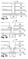
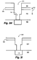
- FIGs. 3A-3J are cross-sectional views showing manufacturing steps of a method for fabricating a multilevel conductive interconnection for an integrated circuit according to a first embodiment of the present invention.
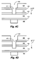
- FIGs. 4A-4G are cross-sectional views showing manufacturing steps of another method for fabricating a multilevel conductive interconnection for an integrated circuit according to a second embodiment of the present invention.
- a semiconductor substrate 300 is provided having a dielectric layer 310 formed thereon.
- the term semiconductor substrate is understood to possibly include a semiconductor wafer, active and passive devices formed within the wafer, and layers formed on the wafer's surface.
- the term semiconductor substrate is meant to include devices formed within a semiconductor wafer and the layers overlying the wafer.
- the dielectric layer 310 may comprise one or more layers of dielectric material which may be formed using techniques well-known in the art such as plasma enhanced chemical vapor deposition (PECVD), chemical vapor deposition (CVD), or spin-on techniques.
- a selective overlayer 320 is formed over the dielectric layer 310 in accordance with the present invention.
- the selective overlayer 320 may be formed using PECVD, CVD, spin-on methods, or any of several other techniques well-known in the art.
- the selective overlayer 320 may comprise any of several dielectric materials, for example, silicon nitride (SiN), amorphous hydrogenated silicon carbide (a-SiC:H), or silicon oxynitride (SiON).
- the selective overlayer material is chosen so that there exists a high degree of selectivity between the selective overlayer 320 and certain of the layers in the dielectric layer 310 , depending, of course on the composition of the dielectric layer.
- the thickness of the selective overlayer 320 may vary depending on factors such as the composition of the dielectric layer 310 and the composition of the selective overlayer 320 , but is typically between 5 and 150 nanometers.
- the selective overlayer 320 provides numerous advantages over the prior art.
- the selective overlayer 320 serves as a protective layer that prevents the upper layer of the dielectric layer 310 from being eroded during the formation of the multilevel interconnects.
- the selective overlayer 320 solves many of the problems associated with the full-via first and partial-via first methods because it allows a relatively deep partial via to be formed while preventing the deposit of undeveloped photoresist in subsequent steps.
- the selective overlayer 320 provides advantages during the planarization and polishing processes because it may be chosen to have a high degree of selectivity with respect to the conductive layer allowing for planarization without loss of trench depth control.
- the selective overlayer 320 may be chosen to provide other advantages as well. For instance, the selective overlayer 320 may be selected so that it has desired optical properties to assist in photolithography processes by reducing the reflectivity of the underlying layers.
- a first patterned photoresist layer 330 is formed over the selective overlayer 320 to define a first opening 340 .
- the dimensions of the first opening may vary widely in accordance with the overall circuit design.
- the first patterned photoresist layer may be formed using any of several well-known photolithography methods.
- the selective overlayer 320 and the dielectric layer 310 are etched using the first patterned photoresist layer 330 as a mask to transfer the first opening 340 through the selective overlayer 320 and into the dielectric layer 310 to a first predetermined depth 350 .
- the first predetermined depth 350 is chosen based on the composition of the dielectric layer 320 and the desired depth of the initial etch. It should, however, be shallow enough to completely develop the photoresist and, thus, preclude undeveloped photoresist from remaining in the bottom or lower portion of the first opening 340 during the subsequent step of forming a second patterned photoresist layer.
- the etching process may be accomplished using any one of several well-known etching techniques including reactive ion etching or high density plasma (HDP) etching.
- the etching chemistry preferably is chosen to minimize the time required to complete the etch.
- a two step etching process may be utilized wherein the first step would etch through the selective overlayer using a suitable etching chemistry such as one comprising fluoromethane (CH 3 F) and oxygen (O 2 ), and the second step would etch the dielectric layer to the first predetermined depth 350 using a suitable etching chemistry such as one comprising perfluorocyclobutane (C 4 F 8 ), carbon monoxide (CO), argon (Ar) and O 2 .
- a suitable etching chemistry such as one comprising perfluorocyclobutane (C 4 F 8 ), carbon monoxide (CO), argon (Ar) and O 2 .
- the first patterned photoresist layer is removed using any of several techniques well-known in the art such as oxygen plasma ashing or by applying a chemical solvent strip.
- a second patterned photoresist layer 360 is then formed over the selective overlayer 320 to define a second opening 370 using any of several well-known photolithography techniques.
- the second opening 370 is shown in FIG. 3E is wider than the first opening 340 , it will be understood that the dimensions of the first and second openings 340 , 370 are determined by the overall circuit design and, thus, the second opening need not be wider than the first opening.
- the dielectric layer 310 is etched to a second predetermined depth 380 using the selective overlayer 320 as a mask to transfer the first opening 340 further into the dielectric layer 310 .
- the selective overlayer 320 prevents the second opening 370 from being transferred into the dielectric layer 310 . This allows a relatively deep first opening 340 to be formed without eroding the upper surface of the dielectric layer 310 and eliminates the possibility that undesired undeveloped photoresist may remain at the bottom of the first opening because the depth of the first opening remained relatively shallow until after the second patterned photoresist layer had been formed.
- the etching of the dielectric layer may be accomplished using any of several well-known techniques such as HDP or reactive ion etching.
- the selective overlayer 320 should have a relatively high degree of selectivity with respect to the portion of the dielectric layer 310 being etched. This high degree of selectivity allows the dielectric layer 310 to be etched at a rate much faster than the selective overlayer 320 is etched. It will be recognized by those skilled in the art that this may be accomplished by choosing an appropriate etching chemistry having the necessary properties based on the composition of the selective overlayer 320 and the dielectric layer 310 .
- the desired etching properties may be obtained using an etching chemistry comprising C 4 F 8 , CO, Ar and O 2 .
- the selective overlayer 320 is etched using the second patterned photoresist layer 360 as a mask to transfer the second opening 370 substantially through the selective overlayer 320 .
- the etching process may be performed using any of several well-known etching techniques such as HDP or reactive ion etching.
- the etching process should have a high degree of selectivity between the selective overlayer 320 and the second patterned photoresist layer 360 so that the second opening 370 can be transferred through the selective overlayer 320 while the second patterned photoresist layer 360 is etched minimally, if at all.
- etching chemistry that etches the selective overlayer 320 at a much faster rate than the second patterned photoresist layer 360 .
- an etching chemistry comprising CH 3 F and O 2 may be used.
- the dielectric layer 310 is etched using the second patterned photoresist layer 360 as a mask to transfer the first opening 340 through the dielectric layer 310 exposing the underlying semiconductor substrate 300 , while, at substantially the same time, the second opening 370 is transferred at least partially into the dielectric layer 310 to a third predetermined depth 390 .
- the third predetermined depth 390 is chosen based on the desired depth of the second opening 370 as dictated by the overall circuit design. This may be accomplished using any of several well-known etching techniques whereby the etching chemistry is chosen such that the portion of the dielectric layer 310 being etched etches at a much faster rate than the selective overlayer 320 .
- an etching chemistry comprising C 4 F 8 , CO, Ar and O 2 may be used.
- the second patterned photoresist layer 360 is then removed using any of several known techniques such as oxygen plasma ashing or applying a chemical solvent strip. It will be understood, however, that the second patterned photoresist layer may be removed prior to the etching step shown in FIG. 3H without altering the novel aspects of the invention.
- a conductive layer 395 preferably comprising a metal such as copper, may be deposited to fill the first and second openings 340 , 370 using techniques well known in the art.
- the completed dual damascene structure is then polished and planarized to remove unwanted portions of the conductive layer 395 extending past the dielectric layer using common techniques such as chemical/mechanical polishing (CMP).
- CMP chemical/mechanical polishing
- the selective overlayer 320 can serve as a polish slowdown during this process, which provides for greater control over the trench depth because a high degree of selectivity is obtainable between the selective overlayer and the conductive layer.
- the selective overlayer 320 also provides the advantage of preventing erosion of the dielectric layer 310 during the polishing process.
- the completed, planarized multilevel interconnect structure with the selective overlayer still intact is shown in FIG. 3J.
- the selective overlayer can be removed after the polishing and planarization process using well-known techniques leaving a conductive contact raised slightly above the dielectric layer.
- the selective overlayer 320 can be removed prior to the deposition of the conductive layer 395 using common etching techniques.
- the conductive layer can then be deposited and polished to cause the conductive layer and the dielectric layer to be substantially coplanar using techniques well known in the art.
- the dielectric layer 310 may comprise a first dielectric layer comprising a first dielectric material formed over a second dielectric layer comprising a second dielectric material.
- the first and second dielectric layers are selected such that they share similar etching characteristics.
- the selective overlayer 320 and the dielectric layer 310 are etched to the first predetermined depth 350 to transfer the first opening 340 at least partially into the first dielectric layer. It will be recognized, however, that the first opening may be transferred through the first dielectric layer and into one or more of the underlying dielectric layers, if desired.
- the dielectric layer 310 is then etched to the second predetermined depth 380 to transfer the first opening 340 through the first dielectric layer and at least partially into the second dielectric layer.
- the dielectric layer 310 is then etched using the selective overlayer as a mask to transfer the first opening 340 through the second dielectric layer while, at the same time, transferring the second opening 370 through the first dielectric layer.
- FIGs. 4A-4G there are shown cross-sectional views illustrating steps of another preferred embodiment of the present invention wherein the dielectric layer comprises a composite layer.
- a semiconductor substrate 400 is provided having a composite layer formed thereon, wherein the composite layer comprises a first dielectric layer 440 , formed over a second dielectric layer 430 , formed over a third dielectric layer 420 , formed over a fourth dielectric layer 410 .
- the first dielectric layer 440 is sometimes referred to as the trench dielectric layer and may comprise SiO 2 or any of several dielectrics with similar properties.
- the second dielectric layer 430 may comprise SiN or any one of several materials with similar characteristics.
- the third dielectric layer 420 sometimes referred to as the via dielectric layer, may comprise SiO 2 , but it will be understood by those skilled in the art that any dielectric material with similar properties may also be used.
- the fourth dielectric layer 410 serves as a diffusion barrier to protect the semiconductor substrate and may comprise any of a variety of materials such as SiN, SiON, or a-SiC:H. Each of the layers of dielectric may be formed using PECVD, CVD, spin-on techniques, or any of several other techniques well-known in the art.
- the first and third dielectric layers 440 , 420 have similar etching characteristics while the second and fourth dielectric layers 430 , 410 also have similar etching characteristics. It is also preferred that there be a high degree of selectivity between the second and fourth dielectric layers 430 , 410 and the first and third dielectric layers 440 , 420 .
- the composite layer may comprise a first dielectric layer comprising SiO 2 , a second dielectric layer comprising SiN, a third dielectric layer comprising SiO 2 , and a fourth dielectric layer comprising SiN.
- each of the dielectric layers may vary depending on the design of the integrated circuit.
- the first and third dielectric layers 440 , 420 may have a thickness between approximately 300 to 900 nanometers while the second and fourth dielectric layers 430 , 410 may have a thickness between approximately 5 to 150 nanometers.
- the second and fourth dielectric layers 440 , 420 have approximately the same thickness.
- an aspect of the present invention is the formation of a selective overlayer 450 over the first dielectric layer 440 .
- the selective overlayer 450 may comprise any of several materials well-known in the art and may be formed using PECVD, CVD, spin-on methods, or other techniques well-known in the art.
- the selective overlayer 450 should be chosen such that it has a high degree of selectivity with respect to the first and third dielectric layers 440 , 420 .
- the selectivity is preferably greater than the thickness of the first dielectric layer divided by the thickness of the selective overlayer.
- the selective overlayer 450 may comprise SiN, a-SiC:H, SiON, or any of several other materials with similar etching characteristics.
- a first patterned photoresist layer 460 is formed over the selective overlayer 450 to define a first opening 470 using any of several photolithography methods well-known in the art.
- the dimensions of the first opening 470 are determined based on the overall circuit design.
- the selective overlayer 450 and the composite layer are etched to a first predetermined depth 480 using the first patterned photoresist layer 460 as a mask to transfer the first opening 470 through the selective overlayer 450 and into one or more of the dielectric layers of the composite layer.
- the etching process may be performed using any of several well-known etching techniques including reactive ion or HDP etching.
- the first predetermined depth 480 should be shallow enough to prevent undeveloped photoresist from remaining in the bottom or lower portion of the first opening after completion of subsequent photolithography steps. It is preferred that the first opening 470 be transferred to a first predetermined depth 480 which is approximately the same as the depth of the upper boundary of the third dielectric layer 420 .
- the first patterned photoresist layer is removed using any of several techniques well-known in the art such as oxygen plasma ashing or by applying a chemical solvent strip.
- a second patterned photoresist layer 490 is formed over the selective overlayer 450 to define a second opening 500 .
- the dimensions of the first and second openings 470 , 500 are determined based on the overall circuit design. Thus, although the second opening 500 shown in FIG. 4C is wider than the first opening 470 , this need not be the case depending on the requirements of the circuit design.
- the composite layer is etched to a second predetermined depth 510 which is greater than the first predetermined depth 480 using the second patterned photoresist layer 490 and the selective overlayer 450 as masks to transfer the first opening 470 further into one or more of the dielectric layers of the composite layer.
- the selective overlayer 450 prevents the second opening 500 from being transferred into the first dielectric layer 440 while still allowing the first opening 470 to be transferred further into the composite layer.
- the composite layer is etched such that the second predetermined depth 510 is between the depth of an upper and lower boundary of the third dielectric layer 420 .
- the second predetermined depth 510 preferably is chosen so that the first opening 470 may be transferred through the third dielectric layer 420 in substantially the same length of etch time as the second opening 500 is transferred through the second dielectric layer 440 in subsequent steps. This may be accomplished by choosing the second predetermined depth 510 such that the difference between the lower boundary of the first dielectric layer 440 and the second predetermined depth 510 is equal to the thickness of the first dielectric layer 440 .
- the etching process may be accomplished by choosing an etching chemistry such that the third dielectric layer 420 etches faster than the selective overlayer.
- a suitable etching solution may comprise C 4 F 8, CO, Ar and O 2 .
- the selective overlayer 450 is then etched using the second patterned photoresist layer 490 as a mask to transfer the second opening 500 through the selective overlayer 450 .
- This etching step may be accomplished using any of several etching techniques known in the art, such as HDP etching, by selecting an etching chemistry such that the selective overlayer 450 is etched at a very high rate while the first and third dielectric layers 440 , 420 are etched minimally, if at all.
- suitable etching chemistry could comprise CH 3 F and O 2 .
- the composite layer is etched using the selective overlayer 450 and the second dielectric layer 430 as masks to transfer the first opening 470 substantially through the third dielectric layer 420 and the second opening 500 substantially through the first dielectric layer 440 .
- This etching step may be accomplished using any of several etching techniques well-known in the art whereby the etching chemistry is chosen such that the first and third dielectric layers 440 , 420 are etched at a much faster rate than the selective overlayer 450 and the second and fourth dielectric layers 430 , 410 .
- first opening 470 to be transferred through the third dielectric layer 420 and the second opening 500 to be transferred through the first dielectric layer 440 while the selective overlayer 450 and the second and fourth dielectric layers 430 , 410 are etched minimally, if at all.
- This may be achieved using any of several well-known etching chemistries to provide the desired etch rates.
- an etching chemistry comprising C 4 F 8 , CO, Ar and O 2 may be used.
- the second patterned photoresist layer 490 is removed using any of several techniques well-known in the art such as oxygen plasma ashing or by applying a chemical solvent strip. It will be recognized, however, that the second patterned photoresist layer may be removed after completion of the dual damascene opening without altering the novel aspects of the present invention as described below.
- the selective overlayer 450 and the composite layer are etched to transfer the first opening 470 substantially through the fourth dielectric layer 410 and the second opening 500 substantially through the second dielectric layer 430 .
- the selective overlayer 450 , the second dielectric layer 430 , and the fourth dielectric layer 410 are selected such that that the three layers may be simultaneously etched to substantially remove the selective overlayer 450 while, at substantially the same time, transferring the first opening 470 through the fourth dielectric layer 410 and the second opening 500 through the second dielectric layer 430 . This may be accomplished by selecting the selective overlayer 450 , the second dielectric layer 430 , and the fourth dielectric layer 410 such that they share substantially the same thickness and substantially the same etching characteristics.
- the selective overlayer 450 and the second and fourth dielectric layers 430 , 410 are selected such that they are etched at a much faster rate than the first and third dielectric layers 440 , 420 .
- the selective overlayer 450 and the second and fourth dielectric layers 430 , 410 may each comprise SiN and the first and third dielectric layers 440 , 420 may comprise SiO 2 .
- the etching step may be performed using an etching chemistry comprising CH 3 F and O 2 .
- the same results may be still be achieved by altering either the thickness or the etching characteristics of the respective layers such that the time required to etch each layer remains substantially the same.
- the selective overlayer could be twice as thick as the second and fourth dielectric layers and still be removed in substantially the same amount of time if the etching chemistry were chosen such that the selective overlayer was etched at twice the rate of the second and fourth dielectric layers.
- a conductive layer (not shown), preferably comprising a metal such as copper, is then deposited to fill the first and second openings. Having removed the selective overlayer 450 , the excess metal may be polished away and the structure planarized to cause the conductive layer to be substantially coplanar with the first dielectric layer 440 using common techniques such as CMP.
- the selective overlayer 450 is chosen such that the etch process removes all but a relatively thin layer of the selective overlayer 450 which remains over the first dielectric layer 440 .
- a conductive layer is then applied as before.
- the excess metal is then polished away and the entire structure is planarized using common techniques such as CMP.
- the thin layer of the selective overlayer 450 may then serve as a polish slowdown during the polishing and planarization process as described in the above embodiments.
- the selective overlayer 450 also prevents erosion of the first dielectric layer 440 .
- the thin layer of the selective overlayer 450 may be removed after the planarization and polishing process leaving a conductive contact raised slightly above the first dielectric layer 440 .
- the steps of the previous preferred embodiment are performed up to the stage depicted in FIG. 4E.
- the composite layer is etched using the second patterned photoresist layer 490 and the second dielectric layer 430 as masks to transfer to the first opening 470 through the fourth dielectric layer 410 and the second opening 500 through the second dielectric layer 430 .
- the second patterned photoresist layer 490 serves as a mask over the selective overlayer 450 such that the selective overlayer 450 is left intact during the etching process.
- the second patterned photoresist layer 490 is then removed to expose the fully-intact selective overlayer 450 .
- a conductive layer is then deposited as before and polished using the selective overlayer 450 as a polish slowdown.
- this embodiment also allows the selective overlayer 450 to remain at approximately the same thickness throughout the formation of the dual damascene structure without requiring any additional etching.
- the selective overlayer 450 may be formed to a desired thickness which is maintained throughout the process.
Landscapes
- Internal Circuitry In Semiconductor Integrated Circuit Devices (AREA)
Applications Claiming Priority (2)
| Application Number | Priority Date | Filing Date | Title |
|---|---|---|---|
| US454909 | 1982-12-30 | ||
| US09/454,909 US6329281B1 (en) | 1999-12-03 | 1999-12-03 | Methods for fabricating a multilevel interconnection for an integrated circuit device utilizing a selective overlayer |
Publications (1)
| Publication Number | Publication Date |
|---|---|
| EP1107308A1 true EP1107308A1 (fr) | 2001-06-13 |
Family
ID=23806570
Family Applications (1)
| Application Number | Title | Priority Date | Filing Date |
|---|---|---|---|
| EP00310512A Withdrawn EP1107308A1 (fr) | 1999-12-03 | 2000-11-27 | Procédé pour la fabrication d'une interconnexion à plusieurs niveaux pour un circuit intégré utilisant une couche protectrice |
Country Status (5)
| Country | Link |
|---|---|
| US (1) | US6329281B1 (fr) |
| EP (1) | EP1107308A1 (fr) |
| JP (1) | JP2001244336A (fr) |
| KR (1) | KR20010062111A (fr) |
| TW (1) | TW465106B (fr) |
Cited By (5)
| Publication number | Priority date | Publication date | Assignee | Title |
|---|---|---|---|---|
| WO2002093641A1 (fr) * | 2001-05-17 | 2002-11-21 | Honeywell International Inc. | Stratifie constitue d'un masque dur et de materiaux dielectriques et procedes de production correspondants |
| EP1351290A3 (fr) * | 2002-03-19 | 2004-12-15 | Texas Instruments Incorporated | Méthode de formation de trous et de tranchées avec une vitesse de gravure de SiC et une sélectivité controllées |
| EP1429382A3 (fr) * | 2002-11-26 | 2008-08-27 | Texas Instruments Incorporated | Formation d'un trou de contact pour conducteurs métalliques damasquines dans un circuit intégré |
| CN100419995C (zh) * | 2005-12-13 | 2008-09-17 | 台湾积体电路制造股份有限公司 | 双镶嵌工艺 |
| DE102007052049A1 (de) * | 2007-10-31 | 2009-05-07 | Advanced Micro Devices, Inc., Sunnyvale | Halbleiterbauelement und Verfahren zum Strukturieren von vertikalen Kontakten und Metallleitungen in einem gemeinsamen Ätzprozess |
Families Citing this family (13)
| Publication number | Priority date | Publication date | Assignee | Title |
|---|---|---|---|---|
| US6605540B2 (en) * | 2001-07-09 | 2003-08-12 | Texas Instruments Incorporated | Process for forming a dual damascene structure |
| KR100419746B1 (ko) * | 2002-01-09 | 2004-02-25 | 주식회사 하이닉스반도체 | 반도체소자의 다층 금속배선 형성방법 |
| US20030134495A1 (en) * | 2002-01-15 | 2003-07-17 | International Business Machines Corporation | Integration scheme for advanced BEOL metallization including low-k cap layer and method thereof |
| US20030190829A1 (en) * | 2002-04-05 | 2003-10-09 | Brennan Kenneth D. | Dual damascene barrier structures and preferential etching method |
| KR100431325B1 (ko) * | 2002-06-28 | 2004-05-12 | 주식회사 하이닉스반도체 | 적층된 에스아이엔을 이용한 구리확산방지막 형성방법 |
| JP4109531B2 (ja) * | 2002-10-25 | 2008-07-02 | 松下電器産業株式会社 | 半導体装置及びその製造方法 |
| KR100917099B1 (ko) * | 2002-12-26 | 2009-09-15 | 매그나칩 반도체 유한회사 | 듀얼 다마신 패턴 형성 방법 |
| KR100599431B1 (ko) * | 2004-07-14 | 2006-07-14 | 주식회사 하이닉스반도체 | 반도체 소자 및 그 제조 방법 |
| KR100641553B1 (ko) * | 2004-12-23 | 2006-11-01 | 동부일렉트로닉스 주식회사 | 반도체 소자에서 패턴 형성 방법 |
| JP4521349B2 (ja) * | 2005-10-13 | 2010-08-11 | 富士通セミコンダクター株式会社 | 半導体集積回路装置 |
| US20090014887A1 (en) * | 2006-01-06 | 2009-01-15 | Nec Corporation | Method of producing multilayer interconnection and multilayer interconnection structure |
| JP4768557B2 (ja) * | 2006-09-15 | 2011-09-07 | 株式会社東芝 | 不揮発性半導体記憶装置及びその製造方法 |
| CN102800626A (zh) * | 2012-08-16 | 2012-11-28 | 上海华力微电子有限公司 | 双大马士革结构介电质膜刻蚀成型工艺的方法 |
Citations (3)
| Publication number | Priority date | Publication date | Assignee | Title |
|---|---|---|---|---|
| US5858877A (en) * | 1992-07-28 | 1999-01-12 | Micron Technology, Inc. | Self-aligned process for making contacts to silicon substrates during the manufacture of integrated circuits therein |
| EP0945900A1 (fr) * | 1998-03-26 | 1999-09-29 | Matsushita Electric Industrial Co., Ltd. | Méthode de formation d'une structure d'interconnexion |
| US6107204A (en) * | 1998-10-02 | 2000-08-22 | Advanced Micro Devices, Inc. | Method to manufacture multiple damascene by utilizing etch selectivity |
Family Cites Families (13)
| Publication number | Priority date | Publication date | Assignee | Title |
|---|---|---|---|---|
| JP2934353B2 (ja) * | 1992-06-24 | 1999-08-16 | 三菱電機株式会社 | 半導体装置およびその製造方法 |
| JPH0697290A (ja) * | 1992-09-17 | 1994-04-08 | Fujitsu Ltd | 半導体装置の製造方法 |
| US5635423A (en) * | 1994-10-11 | 1997-06-03 | Advanced Micro Devices, Inc. | Simplified dual damascene process for multi-level metallization and interconnection structure |
| US5891799A (en) | 1997-08-18 | 1999-04-06 | Industrial Technology Research Institute | Method for making stacked and borderless via structures for multilevel metal interconnections on semiconductor substrates |
| US5822996A (en) | 1997-08-22 | 1998-10-20 | Carrier Corporation | Vapor separation of variable capacity heat pump refrigerant |
| US5877075A (en) | 1997-10-14 | 1999-03-02 | Industrial Technology Research Institute | Dual damascene process using single photoresist process |
| US5935762A (en) | 1997-10-14 | 1999-08-10 | Industrial Technology Research Institute | Two-layered TSI process for dual damascene patterning |
| US6107191A (en) * | 1997-11-07 | 2000-08-22 | Lucent Technologies Inc. | Method of creating an interconnect in a substrate and semiconductor device employing the same |
| US5933761A (en) | 1998-02-09 | 1999-08-03 | Lee; Ellis | Dual damascene structure and its manufacturing method |
| US5939788A (en) | 1998-03-11 | 1999-08-17 | Micron Technology, Inc. | Copper diffusion barrier, aluminum wetting layer and improved methods for filling openings in silicon substrates with cooper |
| US6025259A (en) * | 1998-07-02 | 2000-02-15 | Advanced Micro Devices, Inc. | Dual damascene process using high selectivity boundary layers |
| US5916823A (en) | 1998-10-13 | 1999-06-29 | Worldwide Semiconductor Manufacturing Corporation | Method for making dual damascene contact |
| US6107177A (en) * | 1999-08-25 | 2000-08-22 | Siemens Aktienesellschaft | Silylation method for reducing critical dimension loss and resist loss |
-
1999
- 1999-12-03 US US09/454,909 patent/US6329281B1/en not_active Expired - Lifetime
-
2000
- 2000-11-27 EP EP00310512A patent/EP1107308A1/fr not_active Withdrawn
- 2000-11-27 TW TW089125086A patent/TW465106B/zh active
- 2000-12-04 KR KR1020000072954A patent/KR20010062111A/ko not_active Withdrawn
- 2000-12-04 JP JP2000368900A patent/JP2001244336A/ja active Pending
Patent Citations (3)
| Publication number | Priority date | Publication date | Assignee | Title |
|---|---|---|---|---|
| US5858877A (en) * | 1992-07-28 | 1999-01-12 | Micron Technology, Inc. | Self-aligned process for making contacts to silicon substrates during the manufacture of integrated circuits therein |
| EP0945900A1 (fr) * | 1998-03-26 | 1999-09-29 | Matsushita Electric Industrial Co., Ltd. | Méthode de formation d'une structure d'interconnexion |
| US6107204A (en) * | 1998-10-02 | 2000-08-22 | Advanced Micro Devices, Inc. | Method to manufacture multiple damascene by utilizing etch selectivity |
Cited By (9)
| Publication number | Priority date | Publication date | Assignee | Title |
|---|---|---|---|---|
| WO2002093641A1 (fr) * | 2001-05-17 | 2002-11-21 | Honeywell International Inc. | Stratifie constitue d'un masque dur et de materiaux dielectriques et procedes de production correspondants |
| US6656532B2 (en) | 2001-05-17 | 2003-12-02 | Honeywell International Inc. | Layered hard mask and dielectric materials and methods therefor |
| EP1351290A3 (fr) * | 2002-03-19 | 2004-12-15 | Texas Instruments Incorporated | Méthode de formation de trous et de tranchées avec une vitesse de gravure de SiC et une sélectivité controllées |
| EP1429382A3 (fr) * | 2002-11-26 | 2008-08-27 | Texas Instruments Incorporated | Formation d'un trou de contact pour conducteurs métalliques damasquines dans un circuit intégré |
| CN100419995C (zh) * | 2005-12-13 | 2008-09-17 | 台湾积体电路制造股份有限公司 | 双镶嵌工艺 |
| DE102007052049A1 (de) * | 2007-10-31 | 2009-05-07 | Advanced Micro Devices, Inc., Sunnyvale | Halbleiterbauelement und Verfahren zum Strukturieren von vertikalen Kontakten und Metallleitungen in einem gemeinsamen Ätzprozess |
| US8198190B2 (en) | 2007-10-31 | 2012-06-12 | Globalfoundries Inc. | Semiconductor device and method for patterning vertical contacts and metal lines in a common etch process |
| US8741770B2 (en) | 2007-10-31 | 2014-06-03 | Globalfoundries Inc. | Semiconductor device and method for patterning vertical contacts and metal lines in a common etch process |
| DE102007052049B4 (de) | 2007-10-31 | 2020-06-18 | Globalfoundries Dresden Module One Limited Liability Company & Co. Kg | Verfahren zum Strukturieren von vertikalen Kontakten und Metallleitungen in einem gemeinsamen Ätzprozess |
Also Published As
| Publication number | Publication date |
|---|---|
| JP2001244336A (ja) | 2001-09-07 |
| TW465106B (en) | 2001-11-21 |
| US6329281B1 (en) | 2001-12-11 |
| KR20010062111A (ko) | 2001-07-07 |
Similar Documents
| Publication | Publication Date | Title |
|---|---|---|
| US6329281B1 (en) | Methods for fabricating a multilevel interconnection for an integrated circuit device utilizing a selective overlayer | |
| US5753967A (en) | Damascene process for reduced feature size | |
| US6245663B1 (en) | IC interconnect structures and methods for making same | |
| US6268283B1 (en) | Method for forming dual damascene structure | |
| US5534462A (en) | Method for forming a plug and semiconductor device having the same | |
| US6071809A (en) | Methods for forming high-performing dual-damascene interconnect structures | |
| US6331479B1 (en) | Method to prevent degradation of low dielectric constant material in copper damascene interconnects | |
| US6040243A (en) | Method to form copper damascene interconnects using a reverse barrier metal scheme to eliminate copper diffusion | |
| US6066569A (en) | Dual damascene process for metal layers and organic intermetal layers | |
| KR100366625B1 (ko) | 듀얼 다마신 배선구조의 반도체 소자 및 그 제조방법 | |
| US6309957B1 (en) | Method of low-K/copper dual damascene | |
| CN100372097C (zh) | 制作集成电路中铜互连线的方法 | |
| JP5334616B2 (ja) | 相互接続を作製するための方法 | |
| JP2009135518A (ja) | 相互接続の製造方法 | |
| US7119006B2 (en) | Via formation for damascene metal conductors in an integrated circuit | |
| US6686273B2 (en) | Method of fabricating copper interconnects with very low-k inter-level insulator | |
| US6027994A (en) | Method to fabricate a dual metal-damascene structure in a substrate | |
| JP2003179136A (ja) | デュアルダマシン半導体製造のためのマスク層及び相互接続構造 | |
| US6214745B1 (en) | Method of improving surface planarity of chemical-mechanical polishing operation by forming shallow dummy pattern | |
| US6114235A (en) | Multipurpose cap layer dielectric | |
| US20050176239A1 (en) | Method for making contact making connections | |
| US6900123B2 (en) | BARC etch comprising a selective etch chemistry and a high polymerizing gas for CD control | |
| US6236091B1 (en) | Method of forming a local interconnect with improved etch selectivity of silicon dioxide/silicide | |
| US6204096B1 (en) | Method for reducing critical dimension of dual damascene process using spin-on-glass process | |
| US5633207A (en) | Method of forming a wiring layer for a semiconductor device |
Legal Events
| Date | Code | Title | Description |
|---|---|---|---|
| PUAI | Public reference made under article 153(3) epc to a published international application that has entered the european phase |
Free format text: ORIGINAL CODE: 0009012 |
|
| AK | Designated contracting states |
Kind code of ref document: A1 Designated state(s): AT BE CH CY DE DK ES FI FR GB GR IE IT LI LU MC NL PT SE TR |
|
| AX | Request for extension of the european patent |
Free format text: AL;LT;LV;MK;RO;SI |
|
| RIN1 | Information on inventor provided before grant (corrected) |
Inventor name: DRUMMOND ROBY, MARY Inventor name: VITKAVAGE, DANIEL JOSEPH Inventor name: LYTLE, STEVEN ALAN |
|
| AKX | Designation fees paid |
Inventor name: VITKAVAGE, DANIEL JOSEPH Inventor name: DRUMMOND ROBY, MARY |
|
| REG | Reference to a national code |
Ref country code: DE Ref legal event code: 8566 |
|
| STAA | Information on the status of an ep patent application or granted ep patent |
Free format text: STATUS: THE APPLICATION IS DEEMED TO BE WITHDRAWN |
|
| 18D | Application deemed to be withdrawn |
Effective date: 20011214 |