EP1107328A2 - Stromdetektor mit einer Hall-Effekt-Anordnung - Google Patents
Stromdetektor mit einer Hall-Effekt-Anordnung Download PDFInfo
- Publication number
- EP1107328A2 EP1107328A2 EP00125705A EP00125705A EP1107328A2 EP 1107328 A2 EP1107328 A2 EP 1107328A2 EP 00125705 A EP00125705 A EP 00125705A EP 00125705 A EP00125705 A EP 00125705A EP 1107328 A2 EP1107328 A2 EP 1107328A2
- Authority
- EP
- European Patent Office
- Prior art keywords
- current
- conductor
- hall
- effect device
- current path
- Prior art date
- Legal status (The legal status is an assumption and is not a legal conclusion. Google has not performed a legal analysis and makes no representation as to the accuracy of the status listed.)
- Granted
Links
Images


Classifications
-
- H—ELECTRICITY
- H10—SEMICONDUCTOR DEVICES; ELECTRIC SOLID-STATE DEVICES NOT OTHERWISE PROVIDED FOR
- H10N—ELECTRIC SOLID-STATE DEVICES NOT OTHERWISE PROVIDED FOR
- H10N52/00—Hall-effect devices
- H10N52/101—Semiconductor Hall-effect devices
-
- H—ELECTRICITY
- H10—SEMICONDUCTOR DEVICES; ELECTRIC SOLID-STATE DEVICES NOT OTHERWISE PROVIDED FOR
- H10W—GENERIC PACKAGES, INTERCONNECTIONS, CONNECTORS OR OTHER CONSTRUCTIONAL DETAILS OF DEVICES COVERED BY CLASS H10
- H10W72/00—Interconnections or connectors in packages
- H10W72/851—Dispositions of multiple connectors or interconnections
- H10W72/874—On different surfaces
- H10W72/884—Die-attach connectors and bond wires
-
- H—ELECTRICITY
- H10—SEMICONDUCTOR DEVICES; ELECTRIC SOLID-STATE DEVICES NOT OTHERWISE PROVIDED FOR
- H10W—GENERIC PACKAGES, INTERCONNECTIONS, CONNECTORS OR OTHER CONSTRUCTIONAL DETAILS OF DEVICES COVERED BY CLASS H10
- H10W72/00—Interconnections or connectors in packages
- H10W72/90—Bond pads, in general
- H10W72/941—Dispositions of bond pads
- H10W72/942—Dispositions of bond pads relative to underlying supporting features, e.g. bond pads, RDLs or vias
-
- H—ELECTRICITY
- H10—SEMICONDUCTOR DEVICES; ELECTRIC SOLID-STATE DEVICES NOT OTHERWISE PROVIDED FOR
- H10W—GENERIC PACKAGES, INTERCONNECTIONS, CONNECTORS OR OTHER CONSTRUCTIONAL DETAILS OF DEVICES COVERED BY CLASS H10
- H10W74/00—Encapsulations, e.g. protective coatings
-
- H—ELECTRICITY
- H10—SEMICONDUCTOR DEVICES; ELECTRIC SOLID-STATE DEVICES NOT OTHERWISE PROVIDED FOR
- H10W—GENERIC PACKAGES, INTERCONNECTIONS, CONNECTORS OR OTHER CONSTRUCTIONAL DETAILS OF DEVICES COVERED BY CLASS H10
- H10W90/00—Package configurations
- H10W90/701—Package configurations characterised by the relative positions of pads or connectors relative to package parts
- H10W90/731—Package configurations characterised by the relative positions of pads or connectors relative to package parts of die-attach connectors
- H10W90/736—Package configurations characterised by the relative positions of pads or connectors relative to package parts of die-attach connectors between a chip and a stacked lead frame, conducting package substrate or heat sink
-
- H—ELECTRICITY
- H10—SEMICONDUCTOR DEVICES; ELECTRIC SOLID-STATE DEVICES NOT OTHERWISE PROVIDED FOR
- H10W—GENERIC PACKAGES, INTERCONNECTIONS, CONNECTORS OR OTHER CONSTRUCTIONAL DETAILS OF DEVICES COVERED BY CLASS H10
- H10W90/00—Package configurations
- H10W90/701—Package configurations characterised by the relative positions of pads or connectors relative to package parts
- H10W90/751—Package configurations characterised by the relative positions of pads or connectors relative to package parts of bond wires
- H10W90/756—Package configurations characterised by the relative positions of pads or connectors relative to package parts of bond wires between a chip and a stacked lead frame, conducting package substrate or heat sink
Definitions
- This invention relates to current detectors, particularly to that utilizing a Hall-effect device for obtaining a voltage proportional to the magnitude of the current detected.
- Hall-effect device used herein and in the claims appended hereto is meant the voltage generator built on the familiar Hall effect to give an output voltage in direct proportion to the magnetic field applied. Disposed on a current path, the Hall-effect device will be subjected to the magnetic field that is generated in proportion to the magnitude of the current flowing through the path. The result will be the production of a voltage proportional to the current magnitude.
- This prior art current detector proved to be unsatisfactory, however, in the magnitude of the current that can be carried by the conductor layer. A current of, say, one hundred amperes or more could not possibly be made to flow through it.
- the present invention aims at the provision of a current detector of the type incorporating a Hail-effect device, that is capable of more accurately detecting a current of greater magnitude than heretofore.
- the current detector comprises a Hall-effect device for generating a voltage proportional to magnetic field strength, a first and a second current path terminal for the flow of a current to be detected or measured, and first and second conductor means connected between the first and the second current path terminal for providing a first and a second current path, respectively, therebetween.
- the first and the second conductor means have their resistances predetermined in relation to each other so that the current on the first current path terminal is divided at a predetermined ratio into a first fraction flowing through the first conductor means to the second current path terminal, and a second fraction flowing through the second conductor means to the second current path terminal.
- a conductor included in the second conductor means is so arranged in relation to the Hall-effect device as to cause the same to generate an output voltage proportional to the magnitude of the second fraction of the current flowing through the conductor, and hence to the magnitude of the complete current on the first current path terminal. Also included is an enclosure of electrically insulating material closely enveloping at least the first and the second conductor means.
- the complete current detector is encapsulated in a preferred embodiment to be set forth subsequently, leaving exposed only parts of the current path terminals and other necessary terminals.
- the encapsulation conduces to reduction of a temperature difference between the first and the second conductor means to a minimum.
- the reduction of the temperature difference serves in turn to assure that the current is infallibly divided into the two fractions exactly at the predetermined ratio, such division being essential for accurate measurement of the current magnitude.
- Another advantage of the encapsulation is the mechanical integration of the current paths and the Hall-effect device.
- the enhanced positional stability of these components is believed to diminish errors in current detection.
- the current path terminals will be connected to an external circuit whose current is to be detected, in a manner that will not affect the accuracy of current detection or measurement.
- the Hall-effect device may be conventionally formed in a semiconductor substrate having a main working region where a voltage is generated in response to a magnetic field due to the flow of the second fraction of the current through the conductor of the second conductor means.
- the conductor of the second conductor means may be formed in the shape of a substantially annular strip on the semiconductor substrate via an insulating layer so as to encircle, as seen from above, the main working region of the Hall-effect device.
- the conductor can thus be situated as close as possible to the Hall-effect device and in a manner conductive to higher detection sensitivity.
- the current detector comprises: (a) a Hall-effect device 1 for providing an output voltage indicative of the magnitude of the current Is to be detected or measured; (b) a metal-made baseplate 2; (c) two current path terminals 3 and 4 for carrying the current Is; (d) four lead terminals 6, 7, 8 and 9 for connection of the Hall-effect device 1 to external circuitry; (e) two other terminals 10 and 11 for grounding the baseplate 2; (f) a wire or like conductor 12 bridging the current path terminals 3 and 4 for providing therebetween a first current path for carrying a first division Is 1 of the current Is; (g) two other wires or like conductors 13 and 14 and a conductor layer 15 conjointly providing a second current path between the current path terminals 3 and 4 for carrying a second division Is 2 of the current Is; (h) an insulating plate 16; (i) a shielding layer
- the Hall-effect device is approximately square in shape, having four electrodes 19, 20, 21 and 22 formed adjacent its corners.
- the electrodes 19-22 are electrically connected respectively to the four semiconductor regions 24, 25, 26 and 27 of a semiconductor substrate 23.
- the electrodes 19 and 20 are to be connected to a control current supply circuit, not shown, of well known construction, and the electrodes 21 and 22 to an amplifier, also not shown.
- the semiconductor substrate 23 has four other semiconductor regions 28, 29, 30 and 31 than the aforesaid four semiconductor regions 24-27, as best shown also in FIG. 7.
- the fifth semiconductor region 28 takes the form of an island of cruciate shape, as seen in a plan view as in this figure, in the middle of the p type eighth semiconductor region 31 which occupies most part of the semiconductor substrate 23.
- the first and second semiconductor regions 24 and 25 are of n + type, higher in impurity concentration than the fifth semiconductor region 28, and are formed as islands, spaced from each other along the y axis in FIG. 7, in the fifth semiconductor region 28.
- the first and second electrodes 19 and 20 are in ohmic contact with these semiconductor regions 24 and 25.
- the control current I c is to flow through the fifth semiconductor region 28, either from first 24 to second 25 semiconductor region or the other way around.
- the third and fourth semiconductor regions 26 and 27 lie approximately centrally of the fifth semiconductor region 28 in the direction of the y axis, with a spacing from each other in the direction of the x axis.
- the semiconductor regions 26 and 27 are partly contiguous to the fifth semiconductor region 28, partly to the p type sixth and seventh semiconductor regions 29 and 30, and are in ohmic contact with the third and fourth electrodes 21 and 22.
- the semiconductor regions 29 and 30 are intended to limit the areas of contact of the semiconductor regions 26 and 27 with the semiconductor region 28.
- the semiconductor regions 26 and 27 function to detect the output voltage of the Hall-effect device 1.
- the Hall voltage is to be obtained between the third and fourth semiconductor regions 26 and 27 when the control current I c is made to flow between the semiconductor regions 24 and 25, with a magnetic field perpendicular to the direction of current flow. Therefore, the term "primary operating part" of the Hall-effect device, as used herein and in the claims appended hereto, may be construed as that part of the fifth semiconductor region 28 which lies between the semiconductor regions 24 and 25 and between the semiconductor regions 26 and 27. More broadly, however, the entire semiconductor region 28 may be considered to constitute the primary operating part of the Hail-effect device.
- the semiconductor substrate 23 has a laminar insulation 32 of silicon oxides or the like formed on its top surface, as seen in this figure, and a layer 33 of aluminum or like metal formed on its bottom surface, although the provision of this metal layer is not of absolute necessity.
- the laminar insulation 32 is shown to be composed of two layers or laminae 32 a and 32 b in this embodiment of the invention.
- the four electrodes 19-22 typically of aluminum, have parts sandwiched between the insulating layers 32 a and 32 b . The ends of these parts contact the semiconductor regions 24-27 through windows in the insulating layer 32 a. The other ends of the electrodes 19-22 are exposed through windows in the other insulating layer 32 b .
- the noted conductor layer 15, providing part of the second current path, overlies the insulating layer 32 b .
- FIG. 5 best indicates that the metal-made baseplate 2 is approximately square in shape and, as clearly revealed in FIG. 2 , somewhat larger in size than the Hall-effect device 1.
- the baseplate 2 is designed to serve not only as mechanical support for the Hail-effect device 1 but as heat radiator and, further, as electrostatic shield.
- the baseplate 2 may be fabricated from sheet copper of 0.5 to 1.0 millimeter in thickness with a nickel plating thereon.
- the two terminals 10 and 11 extend from the pair of opposite edges of the baseplate 2 for grounding.
- the current path terminals 3 and 4 extend along one of the other two opposite edges of the baseplate 2, with spacings therefrom and a spacing from each other.
- the terminals 6-9 for connection of the Hall-effect device to external circuitry are also spaced from the baseplate 2. Mechanically, however, the Hall-effect device 1 and the terminals 3, 4, 6-11 are all firmly interconnected by the plastic encapsulation 18, indicated by the broken lines in FIG. 5 , closely enveloping them.
- the baseplate 2 and the terminals 3-11 can all be fabricated from a sheet-metal punching shown FIG. 6 and therein generally designated 40.
- the punching 40 has a frame portion 41 holding the terminals 3, 6, 8 and 10 in their prescribed relative positions, another frame portion 42 likewise holding the terminals 4, 7, 9 and 11, and still another bridge portion 43 interconnecting the foregoing two bridge portions 41 and 42. All the terminals 3, 4 and 6-11 are to be cut off the frame portions 41 and 42 along the dot-and-dash lines after the complete device has been encapsulated.
- FIG. 6 shows a punching portion for the set of terminals of one Hall-effect device, it is understood that in practice a punching is fabricated for the terminals of many such devices.
- the insulating plate 16, FIGS. 1, 2 and 4 is an approximately square piece of sheet ceramic, among other insulating materials, which is slightly larger in size than the Hall-effect device 1. Overlying the baseplate 2 as in FIG. 2, the insulating plate 16 functions to insulate the Hall-effect device 1 from the baseplate and to mechanically support the device.
- the shielding layer 17 is a sheet of magnetic material of approximately the same shape and size therewith.
- Preferred magnetic materials are iron, nickel, cobalt, and like conductors capable of shielding the Hall-effect device from the influence of external electric and magnetic fields.
- the shielding layer 17 may be a lamination of a conductive and a magnetic layer, or it may be made from a nonmagnetic conductor such as copper or from a magnetic insulator such as ferrite.
- the shielding layer 17 is electrically connected to the lead terminal 10 via a wire 17 a as in FIG. 1. In addition to magnetically shielding the Hall-effect device 1, this layer is intended to serve to diminish the magnetic resistance of the path of the magnetic flux created by current flow through the conductor layer 15 forming a major part of the second current path.
- FIGS. 2 and 8 A consideration of FIGS. 2 and 8 will show that the insulating plate 16 with the shielding layer 17 thereon is bonded to the baseplate 2 via an adhesive layer 34.
- the noted metal layer 33 bounding the bottom of the Hall-effect device 1 is secured to the shielding layer 17 via a layer 35 of solder or like conductive bonding agent.
- the electrodes 19-22 of the Hall-effect device 1 are electrically connected as aforesaid to the four semiconductor regions 24-27, respectively, of the semiconductor substrate 23 on the one hand and, on the other hand, to the lead terminals 6-9 via wires 36-39, respectively.
- the wire 12 interconnecting the current path terminals 3 and 4 is for formation of the first. direct current path from terminal 3 to terminal 4.
- This first current path is to carry the first division Is 1 of the current Is to be detected or measured, as that current is divided into Is 1 and Is 2 at the end of the terminal 3.
- a description of the second, indirect current path from terminal 3 to terminal 4, for carrying the second current division Is 2 follows.
- the conductor layer 15 of aluminum or the like is formed on the insulating layers 32 so as to surround, as seen in a plan view, the semiconductor region 28, the broader main working region of the Hall-effect device 1.
- the conductor layer 15 so encircles approximately ninety-five percent of the periphery of the semiconductor region 28 in this particular embodiment.
- the conductor layer 15 should so encircle not less than approximately three quarters of the Hall-effect device 1 in order to make this device sufficiently sensitive to the magnetic field that is generated with the flow of the second current division Is 2 through the conductor layer 15, as will be detailed subsequently.
- the conductor layer 15 has one extremity thereof coupled to the first current path terminal 3 via the aluminum wire 13, and the other extremity thereof coupled to the second current path terminal 4 via the aluminum wire 14, thereby completing the second current path, in parallel with the first current path, for carrying the second current division Is 2 from terminal 3 to terminal 4 via the Hall-effect device 1. So arranged and electrically connected to the current path terminals 3 and 4, the conductor layer 15 is designed to apply to the Hall-effect device 1 the magnetic flux due to the flow of the second current division Is 2 therethrough.
- the current path terminals 3 and 4 may be serially connected to the desired electric circuit. Further the lead terminals 6 and 7 may be connected to the unshown control current supply circuit for causing the control current Ic, FIG. 7, to flow between the semiconductor regions 24 and 25, and the lead terminals 8 and 9 to the unshown amplifier.
- the current Is to be measured will be divided into Is 1 and Is 2 .
- the first division Is 1 will flow from terminal 3 to terminal 4 by way of the wire 12, the first current path.
- the second division Is 2 will flow from terminal 3 to terminal 4 by way of the second path composed of the wire 13, conductor layer 15, and wire 14.
- the magnetic field H will be generated which, according to the Ampere rule, is oriented in the direction indicated by the broken-line arrows in FIG 8.
- This direction of the magnetic field is perpendicular to the direction of the control current Ic in the semiconductor region 28, so that the Hall voltage will be generated between the semiconductor regions 26 and 27, hence between the electrodes 21 and 22, and hence between the lead terminals 8 and 9.
- the Hall voltage is proportional to the strength of the magnetic field H , which in turn is proportional to the magnitude of the current Is , so that this current is detectable from the Hall voltage.
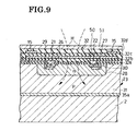
- FIG. 9 shows, in a view similar to FIG. 8, a second preferred form of current detector according to the invention. As will be understood from a comparison of FIGS. 8 and 9 , this second form differs from the first in the following points, the other details of construction being alike in both forms:
- the shielding layer 50 overlies the second insulating layer 32 b so as to cover, as seen from above in FIG. 9 , the semiconductor region 28 and is electrically connected to the electrode 22 to be grounded.
- the insulating layer 32 c is formed as by vapor deposition or sputtering over the second insulating layer 32 b so as to thoroughly cover the shielding layer 50 preformed thereon.
- the conductor layer 15 for carrying the second current division Is 2 is formed on the third insulating layer 32 c in this second embodiment, instead of on the second insulating layer 32 b as in FIG. 8, and thus electrically disconnected from the shielding layer 50.
- the conductor layer 15 is fabricated from gold by plating, vapor deposition, or sputtering to a thickness of from about five to thirteen micrometers.
- the fourth insulating layer 32 d is formed on the third insulating layer 21 c following the formation of the conductor layer 15 thereon.
- the magnetic collector 51 Overlying the fourth insulating layer 32 d is the magnetic collector 51 which is of magnetic material in sheet form that is higher in magnetic permeability than air, examples being ferrite, iron, and nickel.
- the magnetic collector 51 is attached to the fourth insulating layer 32 d , which is of a synthetic adhesive, so as to cover at least all of the semiconductor region 28 as seen from above in FIG. 9 .
- the magnetic collector could be a film of magnetic material formed on the insulating layer 32 d as by vapor deposition or coating.
- This second current detector possesses all but the seventh and eighth of the nine advantages set forth above in conjunction with the first disclosed device. Additional advantages, unique to this second form, are:
Landscapes
- Measuring Instrument Details And Bridges, And Automatic Balancing Devices (AREA)
- Hall/Mr Elements (AREA)
Applications Claiming Priority (2)
| Application Number | Priority Date | Filing Date | Title |
|---|---|---|---|
| JP35006399A JP2001165963A (ja) | 1999-12-09 | 1999-12-09 | ホール素子を備えた電流検出装置 |
| JP35006399 | 1999-12-09 |
Publications (3)
| Publication Number | Publication Date |
|---|---|
| EP1107328A2 true EP1107328A2 (de) | 2001-06-13 |
| EP1107328A3 EP1107328A3 (de) | 2004-10-13 |
| EP1107328B1 EP1107328B1 (de) | 2006-04-12 |
Family
ID=18407987
Family Applications (1)
| Application Number | Title | Priority Date | Filing Date |
|---|---|---|---|
| EP00125705A Expired - Lifetime EP1107328B1 (de) | 1999-12-09 | 2000-11-23 | Stromdetektor mit einer Hall-Effekt-Anordnung |
Country Status (4)
| Country | Link |
|---|---|
| US (1) | US6462531B1 (de) |
| EP (1) | EP1107328B1 (de) |
| JP (1) | JP2001165963A (de) |
| DE (1) | DE60027257T2 (de) |
Cited By (27)
| Publication number | Priority date | Publication date | Assignee | Title |
|---|---|---|---|---|
| WO2002033424A3 (de) * | 2000-10-16 | 2002-11-07 | Vacuumschmelze Gmbh & Co Kg | Anordnung zur potentialfreien messung hoher ströme |
| GB2384317A (en) * | 2001-12-05 | 2003-07-23 | Semikron Ltd | Current sensing using a toroid |
| US6781359B2 (en) | 2002-09-20 | 2004-08-24 | Allegro Microsystems, Inc. | Integrated current sensor |
| EP1267173A3 (de) * | 2001-06-15 | 2005-03-23 | Sanken Electric Co., Ltd. | Hall-Effektstromdetektor |
| WO2005026749A1 (en) * | 2003-08-26 | 2005-03-24 | Allegro Microsystems, Inc. | Current sensor |
| US6995315B2 (en) | 2003-08-26 | 2006-02-07 | Allegro Microsystems, Inc. | Current sensor |
| US7075287B1 (en) | 2003-08-26 | 2006-07-11 | Allegro Microsystems, Inc. | Current sensor |
| WO2006130393A1 (en) * | 2005-05-27 | 2006-12-07 | Allegro Microsystems, Inc. | Current sensor |
| US7166807B2 (en) | 2003-08-26 | 2007-01-23 | Allegro Microsystems, Inc. | Current sensor |
| US7476816B2 (en) | 2003-08-26 | 2009-01-13 | Allegro Microsystems, Inc. | Current sensor |
| US8080994B2 (en) | 2006-05-12 | 2011-12-20 | Allegro Microsystems, Inc. | Integrated current sensor |
| US8629539B2 (en) | 2012-01-16 | 2014-01-14 | Allegro Microsystems, Llc | Methods and apparatus for magnetic sensor having non-conductive die paddle |
| CN103649762A (zh) * | 2011-07-13 | 2014-03-19 | 旭化成微电子株式会社 | 电流传感器用基板以及电流传感器 |
| WO2014114616A1 (de) * | 2013-01-22 | 2014-07-31 | Phoenix Contact Gmbh & Co. Kg | Strommessgerät für stromschienen |
| CN104134747A (zh) * | 2013-05-03 | 2014-11-05 | 远翔科技股份有限公司 | 用于感测电磁感应的半导体结构及其制造方法 |
| US8907437B2 (en) | 2011-07-22 | 2014-12-09 | Allegro Microsystems, Llc | Reinforced isolation for current sensor with magnetic field transducer |
| JP2015064243A (ja) * | 2013-09-24 | 2015-04-09 | 旭化成エレクトロニクス株式会社 | 電流センサ |
| US9190606B2 (en) | 2013-03-15 | 2015-11-17 | Allegro Micosystems, LLC | Packaging for an electronic device |
| US9666788B2 (en) | 2012-03-20 | 2017-05-30 | Allegro Microsystems, Llc | Integrated circuit package having a split lead frame |
| US9812588B2 (en) | 2012-03-20 | 2017-11-07 | Allegro Microsystems, Llc | Magnetic field sensor integrated circuit with integral ferromagnetic material |
| US10234513B2 (en) | 2012-03-20 | 2019-03-19 | Allegro Microsystems, Llc | Magnetic field sensor integrated circuit with integral ferromagnetic material |
| US10345343B2 (en) | 2013-03-15 | 2019-07-09 | Allegro Microsystems, Llc | Current sensor isolation |
| US10991644B2 (en) | 2019-08-22 | 2021-04-27 | Allegro Microsystems, Llc | Integrated circuit package having a low profile |
| US11644485B2 (en) | 2021-10-07 | 2023-05-09 | Allegro Microsystems, Llc | Current sensor integrated circuits |
| US11768230B1 (en) | 2022-03-30 | 2023-09-26 | Allegro Microsystems, Llc | Current sensor integrated circuit with a dual gauge lead frame |
| US11800813B2 (en) | 2020-05-29 | 2023-10-24 | Allegro Microsystems, Llc | High isolation current sensor |
| US11821924B2 (en) | 2022-03-02 | 2023-11-21 | Globalfoundries Singapore Pte. Ltd. | On-chip current sensor |
Families Citing this family (48)
| Publication number | Priority date | Publication date | Assignee | Title |
|---|---|---|---|---|
| JP3852554B2 (ja) * | 1999-12-09 | 2006-11-29 | サンケン電気株式会社 | ホール素子を備えた電流検出装置 |
| JP4164615B2 (ja) * | 1999-12-20 | 2008-10-15 | サンケン電気株式会社 | ホ−ル素子を備えた電流検出装置 |
| EP1273921A1 (de) * | 2001-07-06 | 2003-01-08 | Sanken Electric Co., Ltd. | Hall-Effekt-Stromdetektor |
| EP1281974B1 (de) * | 2001-07-06 | 2007-04-18 | Sanken Electric Co., Ltd. | Hall-Effekt-Stromdetektor |
| JP2003124212A (ja) * | 2001-10-09 | 2003-04-25 | Sanken Electric Co Ltd | 半導体装置およびその製造方法 |
| US7859105B2 (en) * | 2002-04-04 | 2010-12-28 | Hitachi, Ltd. | Power converter, power system provided with same, and mobile body |
| JP2004186439A (ja) * | 2002-12-03 | 2004-07-02 | Sanken Electric Co Ltd | 半導体装置およびその製造方法 |
| JP2004207477A (ja) * | 2002-12-25 | 2004-07-22 | Sanken Electric Co Ltd | ホール素子を有する半導体装置 |
| US7259545B2 (en) * | 2003-02-11 | 2007-08-21 | Allegro Microsystems, Inc. | Integrated sensor |
| US6958548B2 (en) * | 2003-11-19 | 2005-10-25 | Freescale Semiconductor, Inc. | Semiconductor device with magnetically permeable heat sink |
| JP4904427B2 (ja) * | 2005-05-27 | 2012-03-28 | アレグロ・マイクロシステムズ・インコーポレーテッド | 電流センサ |
| JP2007183221A (ja) * | 2006-01-10 | 2007-07-19 | Denso Corp | 電流センサ |
| US7768083B2 (en) * | 2006-01-20 | 2010-08-03 | Allegro Microsystems, Inc. | Arrangements for an integrated sensor |
| US7816905B2 (en) * | 2008-06-02 | 2010-10-19 | Allegro Microsystems, Inc. | Arrangements for a current sensing circuit and integrated current sensor |
| US8093670B2 (en) | 2008-07-24 | 2012-01-10 | Allegro Microsystems, Inc. | Methods and apparatus for integrated circuit having on chip capacitor with eddy current reductions |
| US8063634B2 (en) * | 2008-07-31 | 2011-11-22 | Allegro Microsystems, Inc. | Electronic circuit and method for resetting a magnetoresistance element |
| US7973527B2 (en) | 2008-07-31 | 2011-07-05 | Allegro Microsystems, Inc. | Electronic circuit configured to reset a magnetoresistance element |
| US9222992B2 (en) * | 2008-12-18 | 2015-12-29 | Infineon Technologies Ag | Magnetic field current sensors |
| WO2010122944A1 (ja) * | 2009-04-21 | 2010-10-28 | アルプス電気株式会社 | 磁気センサパッケージ |
| JP2010256316A (ja) * | 2009-04-27 | 2010-11-11 | Kohshin Electric Corp | 電流センサ |
| US20110006763A1 (en) * | 2009-07-07 | 2011-01-13 | Anthonius Bakker | Hall effect current sensor system and associated flip-chip packaging |
| DE102009028956A1 (de) * | 2009-08-28 | 2011-03-03 | Robert Bosch Gmbh | Magnetfeldsensor |
| DE102009045693B4 (de) * | 2009-10-14 | 2017-07-20 | Robert Bosch Gmbh | Mikromechanisches Bauteil für eine Hall-Sensorvorrichtung und Herstellungsverfahren für ein mikromechanisches Bauteil für eine Hall-Sensorvorrichtung |
| US8717016B2 (en) * | 2010-02-24 | 2014-05-06 | Infineon Technologies Ag | Current sensors and methods |
| US8760149B2 (en) | 2010-04-08 | 2014-06-24 | Infineon Technologies Ag | Magnetic field current sensors |
| US8680843B2 (en) | 2010-06-10 | 2014-03-25 | Infineon Technologies Ag | Magnetic field current sensors |
| US8283742B2 (en) | 2010-08-31 | 2012-10-09 | Infineon Technologies, A.G. | Thin-wafer current sensors |
| US9476915B2 (en) | 2010-12-09 | 2016-10-25 | Infineon Technologies Ag | Magnetic field current sensors |
| US8975889B2 (en) | 2011-01-24 | 2015-03-10 | Infineon Technologies Ag | Current difference sensors, systems and methods |
| US8963536B2 (en) | 2011-04-14 | 2015-02-24 | Infineon Technologies Ag | Current sensors, systems and methods for sensing current in a conductor |
| JP5695196B2 (ja) * | 2011-07-13 | 2015-04-01 | 旭化成エレクトロニクス株式会社 | 電流センサ用基板及び電流センサ |
| US9494660B2 (en) | 2012-03-20 | 2016-11-15 | Allegro Microsystems, Llc | Integrated circuit package having a split lead frame |
| US9411025B2 (en) | 2013-04-26 | 2016-08-09 | Allegro Microsystems, Llc | Integrated circuit package having a split lead frame and a magnet |
| US9553208B2 (en) | 2013-09-16 | 2017-01-24 | Infineon Technologies Ag | Current sensor device |
| CN104749393B (zh) * | 2013-12-31 | 2019-08-20 | 森萨塔科技麻省公司 | 一种霍尔传感器装置及其制造方法 |
| US9354284B2 (en) | 2014-05-07 | 2016-05-31 | Allegro Microsystems, Llc | Magnetic field sensor configured to measure a magnetic field in a closed loop manner |
| CN106461705B (zh) * | 2014-06-27 | 2019-04-30 | 旭化成微电子株式会社 | 电流传感器 |
| US9322887B1 (en) | 2014-12-01 | 2016-04-26 | Allegro Microsystems, Llc | Magnetic field sensor with magnetoresistance elements and conductive-trace magnetic source |
| CN105206740A (zh) * | 2015-11-03 | 2015-12-30 | 常州顶芯半导体技术有限公司 | 一种霍尔器件的封装形式 |
| US9810721B2 (en) * | 2015-12-23 | 2017-11-07 | Melexis Technologies Sa | Method of making a current sensor and current sensor |
| US9958482B1 (en) * | 2016-12-20 | 2018-05-01 | Allegro Microsystems, Llc | Systems and methods for a high isolation current sensor |
| US10935612B2 (en) | 2018-08-20 | 2021-03-02 | Allegro Microsystems, Llc | Current sensor having multiple sensitivity ranges |
| JP7289782B2 (ja) | 2019-12-19 | 2023-06-12 | 株式会社東芝 | 電流検出装置 |
| US11320466B1 (en) | 2020-10-29 | 2022-05-03 | Allegro Microsystems, Llc | Differential current sensor |
| US11402409B1 (en) | 2021-03-22 | 2022-08-02 | Allegro Microsystems, Llc | Differential current sensor package |
| US11567108B2 (en) | 2021-03-31 | 2023-01-31 | Allegro Microsystems, Llc | Multi-gain channels for multi-range sensor |
| JP7614992B2 (ja) * | 2021-09-16 | 2025-01-16 | 株式会社東芝 | 電流検出装置 |
| US11994541B2 (en) | 2022-04-15 | 2024-05-28 | Allegro Microsystems, Llc | Current sensor assemblies for low currents |
Family Cites Families (14)
| Publication number | Priority date | Publication date | Assignee | Title |
|---|---|---|---|---|
| NL170069C (nl) * | 1973-06-18 | 1982-09-16 | Philips Nv | Halfgeleiderinrichting met hall-element. |
| JPS537183A (en) | 1976-07-09 | 1978-01-23 | Ichikoh Industries Ltd | Magneto electro transducer |
| FR2619925B1 (fr) * | 1987-08-26 | 1989-12-22 | Bruni Olivier | Dispositif de mesure de courants forts |
| JPH04364472A (ja) | 1991-06-12 | 1992-12-16 | Fuji Electric Co Ltd | 磁電変換装置 |
| DE59109002D1 (de) * | 1991-07-31 | 1998-07-09 | Micronas Intermetall Gmbh | Hallsensor mit Selbstkompensation |
| DE4141386C2 (de) * | 1991-12-16 | 1995-06-29 | Itt Ind Gmbh Deutsche | Hallsensor |
| DE4221385C2 (de) * | 1992-06-30 | 2000-05-11 | Zetex Neuhaus Gmbh | Bauelement zur potentialfreien Strommessung |
| CN1032610C (zh) * | 1992-08-08 | 1996-08-21 | 易明镜 | 线性霍尔电路 |
| DE4410180A1 (de) * | 1994-03-24 | 1995-09-28 | Bosch Gmbh Robert | Stromstärkemeßgerät |
| US6232832B1 (en) * | 1994-07-19 | 2001-05-15 | Honeywell International Inc | Circuit for limiting an output voltage to a percent of a variable supply voltage |
| DE4431703C2 (de) * | 1994-09-06 | 1997-01-30 | Itt Ind Gmbh Deutsche | Magnetfeldsensor mit Hallelement |
| ATE214806T1 (de) * | 1995-02-17 | 2002-04-15 | Siemens Metering Ag | Anordnung zur temperaturkompensation |
| JPH10282156A (ja) | 1997-04-09 | 1998-10-23 | Yasusuke Yamamoto | 電流センサー |
| JPH10293141A (ja) | 1997-04-18 | 1998-11-04 | Yasusuke Yamamoto | 電流センサー |
-
1999
- 1999-12-09 JP JP35006399A patent/JP2001165963A/ja active Pending
-
2000
- 2000-11-16 US US09/713,996 patent/US6462531B1/en not_active Expired - Lifetime
- 2000-11-23 DE DE60027257T patent/DE60027257T2/de not_active Expired - Fee Related
- 2000-11-23 EP EP00125705A patent/EP1107328B1/de not_active Expired - Lifetime
Cited By (45)
| Publication number | Priority date | Publication date | Assignee | Title |
|---|---|---|---|---|
| WO2002033424A3 (de) * | 2000-10-16 | 2002-11-07 | Vacuumschmelze Gmbh & Co Kg | Anordnung zur potentialfreien messung hoher ströme |
| EP1267173A3 (de) * | 2001-06-15 | 2005-03-23 | Sanken Electric Co., Ltd. | Hall-Effektstromdetektor |
| GB2384317B (en) * | 2001-12-05 | 2005-08-31 | Semikron Ltd | Current level sensing |
| GB2384317A (en) * | 2001-12-05 | 2003-07-23 | Semikron Ltd | Current sensing using a toroid |
| US7265531B2 (en) | 2002-09-20 | 2007-09-04 | Allegro Microsystems, Inc. | Integrated current sensor |
| US6781359B2 (en) | 2002-09-20 | 2004-08-24 | Allegro Microsystems, Inc. | Integrated current sensor |
| WO2005026749A1 (en) * | 2003-08-26 | 2005-03-24 | Allegro Microsystems, Inc. | Current sensor |
| US6995315B2 (en) | 2003-08-26 | 2006-02-07 | Allegro Microsystems, Inc. | Current sensor |
| US7075287B1 (en) | 2003-08-26 | 2006-07-11 | Allegro Microsystems, Inc. | Current sensor |
| US7166807B2 (en) | 2003-08-26 | 2007-01-23 | Allegro Microsystems, Inc. | Current sensor |
| US7709754B2 (en) | 2003-08-26 | 2010-05-04 | Allegro Microsystems, Inc. | Current sensor |
| US7476816B2 (en) | 2003-08-26 | 2009-01-13 | Allegro Microsystems, Inc. | Current sensor |
| US7598601B2 (en) | 2003-08-26 | 2009-10-06 | Allegro Microsystems, Inc. | Current sensor |
| EP2157436A1 (de) * | 2005-05-27 | 2010-02-24 | Allegro Microsystems Inc. | Stromsensor |
| WO2006130393A1 (en) * | 2005-05-27 | 2006-12-07 | Allegro Microsystems, Inc. | Current sensor |
| US8080994B2 (en) | 2006-05-12 | 2011-12-20 | Allegro Microsystems, Inc. | Integrated current sensor |
| EP2733496A4 (de) * | 2011-07-13 | 2014-12-24 | Asahi Kasei Microdevices Corp | Stromsensorträger und stromsensor |
| CN103649762A (zh) * | 2011-07-13 | 2014-03-19 | 旭化成微电子株式会社 | 电流传感器用基板以及电流传感器 |
| US9448256B2 (en) | 2011-07-13 | 2016-09-20 | Asahi Kasei Microdevices Corporation | Current sensor substrate and current sensor |
| CN103649762B (zh) * | 2011-07-13 | 2015-09-16 | 旭化成微电子株式会社 | 电流传感器用基板以及电流传感器 |
| US8907437B2 (en) | 2011-07-22 | 2014-12-09 | Allegro Microsystems, Llc | Reinforced isolation for current sensor with magnetic field transducer |
| US8629539B2 (en) | 2012-01-16 | 2014-01-14 | Allegro Microsystems, Llc | Methods and apparatus for magnetic sensor having non-conductive die paddle |
| US9620705B2 (en) | 2012-01-16 | 2017-04-11 | Allegro Microsystems, Llc | Methods and apparatus for magnetic sensor having non-conductive die paddle |
| US10333055B2 (en) | 2012-01-16 | 2019-06-25 | Allegro Microsystems, Llc | Methods for magnetic sensor having non-conductive die paddle |
| US11828819B2 (en) | 2012-03-20 | 2023-11-28 | Allegro Microsystems, Llc | Magnetic field sensor integrated circuit with integral ferromagnetic material |
| US11961920B2 (en) | 2012-03-20 | 2024-04-16 | Allegro Microsystems, Llc | Integrated circuit package with magnet having a channel |
| US11677032B2 (en) | 2012-03-20 | 2023-06-13 | Allegro Microsystems, Llc | Sensor integrated circuit with integrated coil and element in central region of mold material |
| US9666788B2 (en) | 2012-03-20 | 2017-05-30 | Allegro Microsystems, Llc | Integrated circuit package having a split lead frame |
| US9812588B2 (en) | 2012-03-20 | 2017-11-07 | Allegro Microsystems, Llc | Magnetic field sensor integrated circuit with integral ferromagnetic material |
| US11444209B2 (en) | 2012-03-20 | 2022-09-13 | Allegro Microsystems, Llc | Magnetic field sensor integrated circuit with an integrated coil enclosed with a semiconductor die by a mold material |
| US10230006B2 (en) | 2012-03-20 | 2019-03-12 | Allegro Microsystems, Llc | Magnetic field sensor integrated circuit with an electromagnetic suppressor |
| US10234513B2 (en) | 2012-03-20 | 2019-03-19 | Allegro Microsystems, Llc | Magnetic field sensor integrated circuit with integral ferromagnetic material |
| US10916665B2 (en) | 2012-03-20 | 2021-02-09 | Allegro Microsystems, Llc | Magnetic field sensor integrated circuit with an integrated coil |
| WO2014114616A1 (de) * | 2013-01-22 | 2014-07-31 | Phoenix Contact Gmbh & Co. Kg | Strommessgerät für stromschienen |
| US10345343B2 (en) | 2013-03-15 | 2019-07-09 | Allegro Microsystems, Llc | Current sensor isolation |
| US10753963B2 (en) | 2013-03-15 | 2020-08-25 | Allegro Microsystems, Llc | Current sensor isolation |
| US9865807B2 (en) | 2013-03-15 | 2018-01-09 | Allegro Microsystems, Llc | Packaging for an electronic device |
| US9190606B2 (en) | 2013-03-15 | 2015-11-17 | Allegro Micosystems, LLC | Packaging for an electronic device |
| CN104134747A (zh) * | 2013-05-03 | 2014-11-05 | 远翔科技股份有限公司 | 用于感测电磁感应的半导体结构及其制造方法 |
| JP2015064243A (ja) * | 2013-09-24 | 2015-04-09 | 旭化成エレクトロニクス株式会社 | 電流センサ |
| US10991644B2 (en) | 2019-08-22 | 2021-04-27 | Allegro Microsystems, Llc | Integrated circuit package having a low profile |
| US11800813B2 (en) | 2020-05-29 | 2023-10-24 | Allegro Microsystems, Llc | High isolation current sensor |
| US11644485B2 (en) | 2021-10-07 | 2023-05-09 | Allegro Microsystems, Llc | Current sensor integrated circuits |
| US11821924B2 (en) | 2022-03-02 | 2023-11-21 | Globalfoundries Singapore Pte. Ltd. | On-chip current sensor |
| US11768230B1 (en) | 2022-03-30 | 2023-09-26 | Allegro Microsystems, Llc | Current sensor integrated circuit with a dual gauge lead frame |
Also Published As
| Publication number | Publication date |
|---|---|
| EP1107328A3 (de) | 2004-10-13 |
| DE60027257D1 (de) | 2006-05-24 |
| JP2001165963A (ja) | 2001-06-22 |
| US6462531B1 (en) | 2002-10-08 |
| EP1107328B1 (de) | 2006-04-12 |
| DE60027257T2 (de) | 2007-02-01 |
Similar Documents
| Publication | Publication Date | Title |
|---|---|---|
| EP1107328B1 (de) | Stromdetektor mit einer Hall-Effekt-Anordnung | |
| US6812687B1 (en) | Semiconductor current detector of improved noise immunity | |
| US6791313B2 (en) | Electrical current detector having a U-shaped current path and hall-effect device | |
| JP4164626B2 (ja) | ホ−ル素子を備えた電流検出装置 | |
| US6545457B2 (en) | Current detector utilizing hall effect | |
| CN101809457B (zh) | 具有被夹在中间的磁导率层的电流传感器 | |
| US7106046B2 (en) | Current measuring method and current measuring device | |
| US7642768B1 (en) | Current sensor having field screening arrangement including electrical conductors sandwiching magnetic permeability layer | |
| US11519941B2 (en) | Current sensing device having an integrated electrical shield | |
| JP2001339109A (ja) | ホ−ル素子を備えた電流検出装置 | |
| US6781358B2 (en) | Hall-effect current detector | |
| US20240319234A1 (en) | Integrated current sensor with magnetic flux concentrators | |
| JP7382853B2 (ja) | 磁気センサ及び磁気検出方法 | |
| US20220163571A1 (en) | Current sensor | |
| US5874848A (en) | Electric current sensor utilizing a compensating trace configuration | |
| JP4200358B2 (ja) | ホール素子を備えた電流検出装置 | |
| CN120703430A (zh) | 电流传感器及电流测量装置 | |
| WO2025093271A1 (en) | Current transducer with in-plane gradient sensor |
Legal Events
| Date | Code | Title | Description |
|---|---|---|---|
| PUAI | Public reference made under article 153(3) epc to a published international application that has entered the european phase |
Free format text: ORIGINAL CODE: 0009012 |
|
| AK | Designated contracting states |
Kind code of ref document: A2 Designated state(s): AT BE CH CY DE DK ES FI FR GB GR IE IT LI LU MC NL PT SE TR |
|
| AX | Request for extension of the european patent |
Free format text: AL;LT;LV;MK;RO;SI |
|
| PUAL | Search report despatched |
Free format text: ORIGINAL CODE: 0009013 |
|
| AK | Designated contracting states |
Kind code of ref document: A3 Designated state(s): AT BE CH CY DE DK ES FI FR GB GR IE IT LI LU MC NL PT SE TR |
|
| AX | Request for extension of the european patent |
Extension state: AL LT LV MK RO SI |
|
| RIC1 | Information provided on ipc code assigned before grant |
Ipc: 7H 01L 43/06 B Ipc: 7G 01R 15/20 A |
|
| 17P | Request for examination filed |
Effective date: 20050118 |
|
| 17Q | First examination report despatched |
Effective date: 20050215 |
|
| AKX | Designation fees paid |
Designated state(s): DE FR NL |
|
| GRAP | Despatch of communication of intention to grant a patent |
Free format text: ORIGINAL CODE: EPIDOSNIGR1 |
|
| RTI1 | Title (correction) |
Free format text: CURRENT DETECTOR HAVING A HALL-EFFECT DEVICE |
|
| GRAS | Grant fee paid |
Free format text: ORIGINAL CODE: EPIDOSNIGR3 |
|
| GRAA | (expected) grant |
Free format text: ORIGINAL CODE: 0009210 |
|
| AK | Designated contracting states |
Kind code of ref document: B1 Designated state(s): DE FR NL |
|
| PG25 | Lapsed in a contracting state [announced via postgrant information from national office to epo] |
Ref country code: NL Free format text: LAPSE BECAUSE OF FAILURE TO SUBMIT A TRANSLATION OF THE DESCRIPTION OR TO PAY THE FEE WITHIN THE PRESCRIBED TIME-LIMIT Effective date: 20060412 |
|
| REF | Corresponds to: |
Ref document number: 60027257 Country of ref document: DE Date of ref document: 20060524 Kind code of ref document: P |
|
| NLV1 | Nl: lapsed or annulled due to failure to fulfill the requirements of art. 29p and 29m of the patents act | ||
| PLBE | No opposition filed within time limit |
Free format text: ORIGINAL CODE: 0009261 |
|
| STAA | Information on the status of an ep patent application or granted ep patent |
Free format text: STATUS: NO OPPOSITION FILED WITHIN TIME LIMIT |
|
| 26N | No opposition filed |
Effective date: 20070115 |
|
| EN | Fr: translation not filed | ||
| PGFP | Annual fee paid to national office [announced via postgrant information from national office to epo] |
Ref country code: DE Payment date: 20071130 Year of fee payment: 8 |
|
| PG25 | Lapsed in a contracting state [announced via postgrant information from national office to epo] |
Ref country code: FR Free format text: LAPSE BECAUSE OF FAILURE TO SUBMIT A TRANSLATION OF THE DESCRIPTION OR TO PAY THE FEE WITHIN THE PRESCRIBED TIME-LIMIT Effective date: 20070309 |
|
| PG25 | Lapsed in a contracting state [announced via postgrant information from national office to epo] |
Ref country code: FR Free format text: LAPSE BECAUSE OF FAILURE TO SUBMIT A TRANSLATION OF THE DESCRIPTION OR TO PAY THE FEE WITHIN THE PRESCRIBED TIME-LIMIT Effective date: 20060412 |
|
| PG25 | Lapsed in a contracting state [announced via postgrant information from national office to epo] |
Ref country code: DE Free format text: LAPSE BECAUSE OF NON-PAYMENT OF DUE FEES Effective date: 20090603 |