EP1107335A2 - Organische elektrolumineszente Anzeigevorrichtung - Google Patents
Organische elektrolumineszente Anzeigevorrichtung Download PDFInfo
- Publication number
- EP1107335A2 EP1107335A2 EP00309143A EP00309143A EP1107335A2 EP 1107335 A2 EP1107335 A2 EP 1107335A2 EP 00309143 A EP00309143 A EP 00309143A EP 00309143 A EP00309143 A EP 00309143A EP 1107335 A2 EP1107335 A2 EP 1107335A2
- Authority
- EP
- European Patent Office
- Prior art keywords
- electrode
- organic
- layer
- metal
- metal electrode
- Prior art date
- Legal status (The legal status is an assumption and is not a legal conclusion. Google has not performed a legal analysis and makes no representation as to the accuracy of the status listed.)
- Withdrawn
Links
Images


Classifications
-
- H—ELECTRICITY
- H05—ELECTRIC TECHNIQUES NOT OTHERWISE PROVIDED FOR
- H05B—ELECTRIC HEATING; ELECTRIC LIGHT SOURCES NOT OTHERWISE PROVIDED FOR; CIRCUIT ARRANGEMENTS FOR ELECTRIC LIGHT SOURCES, IN GENERAL
- H05B33/00—Electroluminescent light sources
- H05B33/12—Light sources with substantially two-dimensional [2D] radiating surfaces
- H05B33/26—Light sources with substantially two-dimensional [2D] radiating surfaces characterised by the composition or arrangement of the conductive material used as an electrode
-
- H—ELECTRICITY
- H10—SEMICONDUCTOR DEVICES; ELECTRIC SOLID-STATE DEVICES NOT OTHERWISE PROVIDED FOR
- H10K—ORGANIC ELECTRIC SOLID-STATE DEVICES
- H10K59/00—Integrated devices, or assemblies of multiple devices, comprising at least one organic light-emitting element covered by group H10K50/00
- H10K59/80—Constructional details
- H10K59/805—Electrodes
- H10K59/8051—Anodes
- H10K59/80516—Anodes combined with auxiliary electrodes, e.g. ITO layer combined with metal lines
Definitions
- the present invention relates generally to an organic EL display device using an organic compound, and specifically to an improvement in or relating to an electrode for injecting holes in a light emitting layer.
- the material for the hole injecting electrode in such an organic EL device is that it be transparent and electrically conductive because the organic EL device is usually designed to extract the emitted light from a substrate side thereof.
- ITO, IZO, ZnO, SnO 2 , In 2 O 3 , etc. have been known for such transparent electrodes.
- ITO electrodes have a visible light transmittance of 80% or greater and a sheet resistance of 10 ⁇ / ⁇ or less, and so find wide applications as transparent electrodes for LCDs, solar batteries and so on.
- the ITO electrodes are also considered to be promising for hole injecting electrodes in the organic EL devices.
- An organic EL device requires a given current for light emission, and the light emission luminance increases in proportion to an applied current density. Consequently, when sophisticated display patterns or large-screen displays are driven with high luminance or at high duty ratios, the resistance of interconnecting lines in the hole injecting electrode is found to give rise to voltage drop problems in conjunction with transparent electrodes such as hole injecting electrodes or electrode structures joined thereto, although this resistance is negligible when the length of interconnecting lines is short.
- JP-A's 10-162961, 10-199680, 10-214684, 10-223374, 11-31590, 11-144877, etc. have proposed to locate a metal electrode contiguous to the transparent electrode. According to these proposals, Ni, Cu, Cr, Ti, Fe, Co, Au, Ag, Al, Pt, Rh, Pd and Sn as well as their alloys may be used for such a metal electrode.
- a Cr buffer layer is referred to in JP-A 10-199680; Cr, Ti, and Ti-N buffer layers in JP-A 11-31590, and Mo, and Ni buffer layers in JP-A 11-144877).
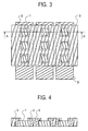
- Fig. 1 is a plan view of the first embodiment of the present invention, wherein the relations between the metal electrode and the pixels (ITO) are illustrated.
- Such a transparent electrode is usually used as an anode or hole injecting electrode.
- the metal electrode (interconnecting electrode) has a sheet resistance of preferably 1 ⁇ / ⁇ or less, and especially 0.5 ⁇ / ⁇ or less. Although there is no lower limit to sheet resistance, a sheet resistance of about 0.1 ⁇ / ⁇ is generally preferred.
- the metal electrode has a thickness of the order of preferably 10 to 2,000 nm, especially 20 to 1,000 nm, and more especially 100 to 500 nm.
- the metal electrode is formed of an alloy containing as the main component Ag, Cu or Ag-Cu and as the first subordinate component one or two or more metal elements selected from the group consisting of Pd, In, Pt and Au. It is preferable that the alloy contains both Ag and Cu as the main components. In this case, Cu should account for preferably 0.1 to 5% by weight, more preferably 0.3 to 3% by weight, and even more preferably 0.5 to 2.0% by weight of all components. By the proper addition of Cu to Ag improvements in corrosion resistance are achievable. However, too little Cu makes its effect slender and too much causes element segregation.
- the metal electrode according to the present invention may contain as the second subordinate component one or two or more metal elements selected from the group consisting of Ti, V, Cr, Mn, Fe, Co, Ni, Nb, Mo, Ta and W.
- the total amount of these metal elements should be preferably 0.1 to 5% by weight, more preferably 0.3 to 3.0% by weight, and even more preferably 0.5 to 2.0% by weight with respect to all components.
- a metal electrode 2 is formed and positioned laterally of an ITO pattern 1 that is the transparent electrode, and an insulating layer 3 is provided in such a way as to cover these parts.
- the insulating layer 3 has an opening in an ITO area defining a pixel area.
- an organic EL structure such as an organic layer.
- the auxiliary electrode is needed although depending on display size and auxiliary electrode material.
- the upper limit to the sheet resistance is a few hundreds ⁇ / ⁇ .
- the electron injecting electrode used has a thickness of usually 300 nm or less, and especially 200 nm or less, too, it is necessary to use the auxiliary electrode, although depending on display size and auxiliary electrode material.
- the thickness of the light emitting layer, the hole injecting and transporting layer, and the electron injecting and transporting layer is not critical and varies with a particular formation technique although it is usually of the order of preferably 5 to 500 nm, and especially 10 to 300 nm.
- the fluorescent compound is used in combination with a host substance capable of emitting light by itself; that is, it is preferable that the fluorescent compound is used as a dopant.
- the content of the fluorescent compound in the light emitting layer is in the range of preferably 0.01 to 10% by weight, and especially 0.1 to 5% by weight.
- Quinolinolato complexes and aluminum complexes containing 8-quinolinol or its derivatives as ligands are preferred for the host substance.
- Such aluminum complexes are typically disclosed in JP-A's 63-264692, 3-255190, 5-70733, 5-258859, 6-215874, etc.
- metal complexes containing quinoline derivatives especially 8-quinolinol or its derivatives as ligands, in particular, tris(8-quinolinolato) aluminum (Alq3).
- quinoline derivatives especially 8-quinolinol or its derivatives
- Alq3 tris(8-quinolinolato) aluminum
- phenylanthracene derivatives and tetraarylethene derivatives.
- the ratio of mixing the compound capable of injecting and transporting holes with the compound capable of injecting and transporting electrons is determined while the carrier mobility and carrier density are taken into consideration.
- the weight ratio between the compound capable of injecting and transporting holes and the compound capable of injecting and transporting electrons is of the order of 1/99 to 99/1, particularly 10/90 to 90/10, and more particularly 20/80 to 80/20.
- the hole injecting and transporting layer is provided as a separate hole injecting layer and a separate hole transporting layer
- two or more compounds are selected in a preferable combination from the compounds already mentioned for the hole injecting and transporting layer.
- ITO hole injecting electrode
- the electron injecting and transporting layer there may be used quinoline derivatives such as organic metal complexes containing 8-quinolinol or its derivatives as ligands, for instance, tris(8-quinolinolato)aluminum (Alq3), oxadiazole derivatives, perylene derivatives, pyridine derivatives, pyrimidine derivatives, quinoxaline derivative, diphenylquinone derivatives, and nitro-substituted fluorene derivatives.
- the electron injecting and transporting layer may also serve as a light emitting layer. In this case, it is preferable to use tris(8-quinolilato)aluminum, etc. As is the case with the light emitting layer, the electron injecting and transporting layer may then be formed by evaporation or the like.
- the electron injecting and transporting layer is a double-layered structure comprising an electron injecting layer and an electron transporting layer
- two or more compounds are selected in a preferably combination from the compounds commonly used for electron injecting and transporting layers.
- an evaporation rate of the order of 0.01 to 1 nm/sec. is preferably applied at a degree of vacuum of 10 -4 Pa or lower. It is also preferable to form the layers continuously in vacuum. If the layers are continuously formed in vacuum, high properties are then obtained because the adsorption of impurities on the interface between the adjacent layers can be avoided. Furthermore, the driving voltage of the device can be lowered while the occurrence and growth of dark spots are inhibited.
- the spacer may have been incorporated in the sealing adhesive agent or may be incorporated in the sealing adhesive agent at the time of bonding.
- the content of the spacer in the sealing adhesive agent should be preferably 0.01 to 30 wt%, and more preferably 0.1 to 5 wt%.
- the organic EL display device of the present invention is generally of the DC or pulse drive type while it may be of the AC drive type.
- the applied voltage is generally of the order of 2 to 30 volts.
- Example 2 An organic EL device was obtained as in Example 2 with the exception that instead of Ag-Pd, a Cu-Pd (Pd: 2.5% by weight) alloy was used as the metal electrode. At this time, the hole injecting electrode had an interconnecting resistance of 300 ⁇ per line. The obtained organic EL device was driven and estimated as in Example 2. The results were substantially the same as in Example 2.
- Example 8 An organic EL device was obtained as in Example 8 with the exception that an IZO transparent electrode was used as the transparent electrode. The obtained organic EL device was driven and estimated as in Example 8. The results were much the same as in Example 8.
Landscapes
- Electroluminescent Light Sources (AREA)
Applications Claiming Priority (2)
| Application Number | Priority Date | Filing Date | Title |
|---|---|---|---|
| JP33993699A JP2001155867A (ja) | 1999-11-30 | 1999-11-30 | 有機el表示装置 |
| JP33993699 | 1999-11-30 |
Publications (1)
| Publication Number | Publication Date |
|---|---|
| EP1107335A2 true EP1107335A2 (de) | 2001-06-13 |
Family
ID=18332171
Family Applications (1)
| Application Number | Title | Priority Date | Filing Date |
|---|---|---|---|
| EP00309143A Withdrawn EP1107335A2 (de) | 1999-11-30 | 2000-10-17 | Organische elektrolumineszente Anzeigevorrichtung |
Country Status (4)
| Country | Link |
|---|---|
| EP (1) | EP1107335A2 (de) |
| JP (1) | JP2001155867A (de) |
| KR (1) | KR20010051823A (de) |
| TW (1) | TW471241B (de) |
Cited By (12)
| Publication number | Priority date | Publication date | Assignee | Title |
|---|---|---|---|---|
| DE10133686A1 (de) * | 2001-07-11 | 2003-01-30 | Osram Opto Semiconductors Gmbh | Organisches, elektrolumineszierendes Display und dessen Herstellung |
| DE10133685A1 (de) * | 2001-07-11 | 2003-01-30 | Osram Opto Semiconductors Gmbh | Organisches, elektrolumineszierendes Display und dessen Herstellung |
| WO2004023575A1 (en) * | 2002-09-05 | 2004-03-18 | Koninklijke Philips Electronics N.V. | Electroluminescent display devices |
| EP1629542A2 (de) * | 2003-05-30 | 2006-03-01 | Schott AG | VERFAHREN ZUR HERSTELLUNG VON OLEDs |
| EP1653517A2 (de) | 2004-10-29 | 2006-05-03 | Lg Electronics Inc. | Organische elektrolumineszente Anzeigevorrichtung und Verfahren zu deren Herstellung |
| EP1286395A3 (de) * | 2001-08-21 | 2006-10-25 | Lg Electronics Inc. | Organische elektrolumineszente Vorrichtung |
| EP1286397A3 (de) * | 2001-08-21 | 2006-10-25 | Lg Electronics Inc. | Organische elektrolumineszente Anzeigevorrichtung und Herstellungsverfahren |
| EP1422977A4 (de) * | 2001-08-31 | 2009-06-17 | Sony Corp | Organisches elektrolumineszenzbauelement und verfahren zu seiner herstellung |
| US7737630B2 (en) | 2002-08-09 | 2010-06-15 | Semiconductor Energy Laboratory Co., Ltd. | Electroluminescence element and a light emitting device using the same |
| EP1608017B1 (de) * | 2004-06-14 | 2016-08-10 | LG Display Co., Ltd. | Organische elektrolumineszente Anzeigevorrichtung und Herstellungsverfahren |
| CN115485818A (zh) * | 2020-06-30 | 2022-12-16 | 株式会社爱发科 | 金属布线结构体、金属布线结构体的制造方法及溅射靶 |
| CN115643770A (zh) * | 2022-11-01 | 2023-01-24 | 四川京龙光电科技有限公司 | 抗冲压的阵列型柔性可拉伸显示组件及其制备方法 |
Families Citing this family (5)
| Publication number | Priority date | Publication date | Assignee | Title |
|---|---|---|---|---|
| JP4434411B2 (ja) * | 2000-02-16 | 2010-03-17 | 出光興産株式会社 | アクティブ駆動型有機el発光装置およびその製造方法 |
| JP4816851B2 (ja) * | 2001-07-26 | 2011-11-16 | 凸版印刷株式会社 | El素子及び表示媒体 |
| JP4997688B2 (ja) | 2003-08-19 | 2012-08-08 | セイコーエプソン株式会社 | 電極、薄膜トランジスタ、電子回路、表示装置および電子機器 |
| TWI305284B (en) * | 2003-12-02 | 2009-01-11 | Chi Mei Optoelectronics Corp | Display device |
| KR100972290B1 (ko) * | 2004-02-04 | 2010-07-23 | 사천홍시현시기건유한공사 | 유기전계발광소자 |
-
1999
- 1999-11-30 JP JP33993699A patent/JP2001155867A/ja active Pending
-
2000
- 2000-10-17 EP EP00309143A patent/EP1107335A2/de not_active Withdrawn
- 2000-10-21 TW TW089122172A patent/TW471241B/zh not_active IP Right Cessation
- 2000-11-20 KR KR1020000069016A patent/KR20010051823A/ko not_active Ceased
Cited By (24)
| Publication number | Priority date | Publication date | Assignee | Title |
|---|---|---|---|---|
| DE10133685A1 (de) * | 2001-07-11 | 2003-01-30 | Osram Opto Semiconductors Gmbh | Organisches, elektrolumineszierendes Display und dessen Herstellung |
| DE10133686C2 (de) * | 2001-07-11 | 2003-07-17 | Osram Opto Semiconductors Gmbh | Organisches, elektrolumineszierendes Display und dessen Herstellung |
| DE10133686A1 (de) * | 2001-07-11 | 2003-01-30 | Osram Opto Semiconductors Gmbh | Organisches, elektrolumineszierendes Display und dessen Herstellung |
| US7417371B2 (en) | 2001-07-11 | 2008-08-26 | Osram Opto Semiconductors Gmbh | Organic electroluminescent device and the production thereof |
| US7375461B2 (en) | 2001-07-11 | 2008-05-20 | Osram Opto Semiconductors Gmbh | Organic, electroluminescent display and method for producing the same |
| DE10133685B4 (de) * | 2001-07-11 | 2006-05-18 | Osram Opto Semiconductors Gmbh | Organisches, elektrolumineszierendes Display und dessen Herstellung |
| EP1286397A3 (de) * | 2001-08-21 | 2006-10-25 | Lg Electronics Inc. | Organische elektrolumineszente Anzeigevorrichtung und Herstellungsverfahren |
| EP1286395A3 (de) * | 2001-08-21 | 2006-10-25 | Lg Electronics Inc. | Organische elektrolumineszente Vorrichtung |
| EP1422977A4 (de) * | 2001-08-31 | 2009-06-17 | Sony Corp | Organisches elektrolumineszenzbauelement und verfahren zu seiner herstellung |
| US9722201B2 (en) | 2001-08-31 | 2017-08-01 | Sony Corporation | Organic electroluminescence device and method of manufacturing the same |
| US10522781B2 (en) | 2001-08-31 | 2019-12-31 | Sony Corporation | Electroluminescence device and display device |
| US10020460B2 (en) | 2001-08-31 | 2018-07-10 | Sony Corporation | Electroluminescence device and display device |
| US8937428B2 (en) | 2001-08-31 | 2015-01-20 | Sony Corporation | Organic electroluminescence device with silver alloy anode and method of manufacturing the same |
| US9240564B2 (en) | 2001-08-31 | 2016-01-19 | Sony Corporation | Organic electroluminescence device and method of manufacturing the same |
| US7737630B2 (en) | 2002-08-09 | 2010-06-15 | Semiconductor Energy Laboratory Co., Ltd. | Electroluminescence element and a light emitting device using the same |
| WO2004023575A1 (en) * | 2002-09-05 | 2004-03-18 | Koninklijke Philips Electronics N.V. | Electroluminescent display devices |
| EP1629542A2 (de) * | 2003-05-30 | 2006-03-01 | Schott AG | VERFAHREN ZUR HERSTELLUNG VON OLEDs |
| CN100557853C (zh) * | 2003-05-30 | 2009-11-04 | 肖特股份公司 | 制造oled的方法 |
| EP1608017B1 (de) * | 2004-06-14 | 2016-08-10 | LG Display Co., Ltd. | Organische elektrolumineszente Anzeigevorrichtung und Herstellungsverfahren |
| EP1653517A3 (de) * | 2004-10-29 | 2007-10-24 | Lg Electronics Inc. | Organische elektrolumineszente Anzeigevorrichtung und Verfahren zu deren Herstellung |
| US7868330B2 (en) | 2004-10-29 | 2011-01-11 | Lg Electronics Inc. | Organic electro-luminescence display device and fabricating method thereof |
| EP1653517A2 (de) | 2004-10-29 | 2006-05-03 | Lg Electronics Inc. | Organische elektrolumineszente Anzeigevorrichtung und Verfahren zu deren Herstellung |
| CN115485818A (zh) * | 2020-06-30 | 2022-12-16 | 株式会社爱发科 | 金属布线结构体、金属布线结构体的制造方法及溅射靶 |
| CN115643770A (zh) * | 2022-11-01 | 2023-01-24 | 四川京龙光电科技有限公司 | 抗冲压的阵列型柔性可拉伸显示组件及其制备方法 |
Also Published As
| Publication number | Publication date |
|---|---|
| KR20010051823A (ko) | 2001-06-25 |
| TW471241B (en) | 2002-01-01 |
| JP2001155867A (ja) | 2001-06-08 |
Similar Documents
| Publication | Publication Date | Title |
|---|---|---|
| US6320311B2 (en) | Organic EL device having a hole injecting electrode including a transparent electrode and a metal electrode | |
| US6469437B1 (en) | Highly transparent organic light emitting device employing a non-metallic cathode | |
| US6200695B1 (en) | Organic electroluminescent device | |
| JP3875401B2 (ja) | 有機el表示装置及び有機el素子 | |
| US6281627B1 (en) | Organic electroluminescent device with a high resistant inorganic electron injecting layer | |
| EP1107335A2 (de) | Organische elektrolumineszente Anzeigevorrichtung | |
| JP3758369B2 (ja) | 有機el表示装置とその製造方法 | |
| US6252246B1 (en) | Organic electroluminescent device | |
| US6166488A (en) | Organic electroluminescent device | |
| EP1079669A1 (de) | Organische elektrolumineszente vorrichtung | |
| US6303239B1 (en) | Organic electroluminescent device | |
| JP4255041B2 (ja) | 有機el素子 | |
| EP1022789A2 (de) | Organische elektrolumineszente Vorrichtung | |
| US6222314B1 (en) | Organic electoluminescent device with inorganic insulating hole injecting layer | |
| EP0892587A2 (de) | Organische elektrolumineszente Vorrichtung und Verfahren zur Herstellung derselben | |
| US6262433B1 (en) | Organic electroluminescent device | |
| JP2001035667A (ja) | 有機el素子 | |
| US6187457B1 (en) | Organic EL element and method of producing the same | |
| US6296954B1 (en) | Organic electroluminescent device | |
| US6338908B1 (en) | Organic electroluminescent device | |
| JPH11135264A (ja) | 有機el素子 | |
| EP0967668A2 (de) | Organische elektrolumineszente Vorrichtung | |
| JP4142779B2 (ja) | 有機el素子 | |
| JP4228021B2 (ja) | 有機el素子 | |
| JPH11354276A (ja) | 発光/表示素子 |
Legal Events
| Date | Code | Title | Description |
|---|---|---|---|
| PUAI | Public reference made under article 153(3) epc to a published international application that has entered the european phase |
Free format text: ORIGINAL CODE: 0009012 |
|
| AK | Designated contracting states |
Kind code of ref document: A2 Designated state(s): AT BE CH CY DE DK ES FI FR GB GR IE IT LI LU MC NL PT SE |
|
| AX | Request for extension of the european patent |
Free format text: AL;LT;LV;MK;RO;SI |
|
| STAA | Information on the status of an ep patent application or granted ep patent |
Free format text: STATUS: THE APPLICATION HAS BEEN WITHDRAWN |
|
| 18W | Application withdrawn |
Withdrawal date: 20020412 |
|
| R18W | Application withdrawn (corrected) |
Effective date: 20020412 |