EP1107456A2 - Verfahren zum Regeln der von einem frequenzsteuerbaren Oszillator abgegebenen Ausgangsfrequenz - Google Patents
Verfahren zum Regeln der von einem frequenzsteuerbaren Oszillator abgegebenen Ausgangsfrequenz Download PDFInfo
- Publication number
- EP1107456A2 EP1107456A2 EP00124958A EP00124958A EP1107456A2 EP 1107456 A2 EP1107456 A2 EP 1107456A2 EP 00124958 A EP00124958 A EP 00124958A EP 00124958 A EP00124958 A EP 00124958A EP 1107456 A2 EP1107456 A2 EP 1107456A2
- Authority
- EP
- European Patent Office
- Prior art keywords
- frequency
- oscillator
- output
- adjustment
- tuning
- Prior art date
- Legal status (The legal status is an assumption and is not a legal conclusion. Google has not performed a legal analysis and makes no representation as to the accuracy of the status listed.)
- Granted
Links
Images


Classifications
-
- H—ELECTRICITY
- H03—ELECTRONIC CIRCUITRY
- H03L—AUTOMATIC CONTROL, STARTING, SYNCHRONISATION OR STABILISATION OF GENERATORS OF ELECTRONIC OSCILLATIONS OR PULSES
- H03L7/00—Automatic control of frequency or phase; Synchronisation
- H03L7/06—Automatic control of frequency or phase; Synchronisation using a reference signal applied to a frequency- or phase-locked loop
- H03L7/08—Details of the phase-locked loop
- H03L7/099—Details of the phase-locked loop concerning mainly the controlled oscillator of the loop
-
- H—ELECTRICITY
- H03—ELECTRONIC CIRCUITRY
- H03L—AUTOMATIC CONTROL, STARTING, SYNCHRONISATION OR STABILISATION OF GENERATORS OF ELECTRONIC OSCILLATIONS OR PULSES
- H03L7/00—Automatic control of frequency or phase; Synchronisation
- H03L7/06—Automatic control of frequency or phase; Synchronisation using a reference signal applied to a frequency- or phase-locked loop
- H03L7/16—Indirect frequency synthesis, i.e. generating a desired one of a number of predetermined frequencies using a frequency- or phase-locked loop
- H03L7/18—Indirect frequency synthesis, i.e. generating a desired one of a number of predetermined frequencies using a frequency- or phase-locked loop using a frequency divider or counter in the loop
- H03L7/183—Indirect frequency synthesis, i.e. generating a desired one of a number of predetermined frequencies using a frequency- or phase-locked loop using a frequency divider or counter in the loop a time difference being used for locking the loop, the counter counting between fixed numbers or the frequency divider dividing by a fixed number
- H03L7/187—Indirect frequency synthesis, i.e. generating a desired one of a number of predetermined frequencies using a frequency- or phase-locked loop using a frequency divider or counter in the loop a time difference being used for locking the loop, the counter counting between fixed numbers or the frequency divider dividing by a fixed number using means for coarse tuning the voltage controlled oscillator of the loop
- H03L7/189—Indirect frequency synthesis, i.e. generating a desired one of a number of predetermined frequencies using a frequency- or phase-locked loop using a frequency divider or counter in the loop a time difference being used for locking the loop, the counter counting between fixed numbers or the frequency divider dividing by a fixed number using means for coarse tuning the voltage controlled oscillator of the loop comprising a D/A converter for generating a coarse tuning voltage
-
- H—ELECTRICITY
- H03—ELECTRONIC CIRCUITRY
- H03L—AUTOMATIC CONTROL, STARTING, SYNCHRONISATION OR STABILISATION OF GENERATORS OF ELECTRONIC OSCILLATIONS OR PULSES
- H03L2207/00—Indexing scheme relating to automatic control of frequency or phase and to synchronisation
- H03L2207/06—Phase locked loops with a controlled oscillator having at least two frequency control terminals
Definitions
- the invention relates to a method for regulating the output frequency output by a frequency controllable oscillator according to the preamble of claim 1 as well to a frequency controllable oscillator according to the preamble of claim 13.
- the output frequency is known to the oscillator of the oscillator 1 in a frequency controller, for example a phase detector 2, with one from a reference frequency oscillator 24 given reference frequency compare and the phase deviation of a frequency actuator of the oscillator as a manipulated variable in the form of a Designated control voltage, control frequency or to supply the like.
- the frequency actuator can an electrically tunable coil, a capacitance diode and / or a mechanically adjustable capacitor or the like exist.
- the object of the present invention is a method to control the output from a frequency controllable oscillator Specify output frequency and a frequency controllable Create oscillator in which a mismatch as well as the need for manual or electrical Adjustment during manufacture and commissioning excluded and is not a re-adjustment due to environmental and Aging influences are required.
- the solution according to the invention is closed by the regulation an electrically or mechanically adjustable frequency actuator a mismatch as well as the need manual or electrical adjustment during manufacture and commissioning an oscillator and requires no readjustment due to short-term fluctuations of the optimal adjustment value, e.g. due to changes in supply voltage or due to temperature influences, or due to long-term changes, for example due to aging frequency-determining Components.
- the solution according to the invention is based on the basic idea the distance between the frequency-determining control variable taking into account the extreme operating frequencies the limits given by the operating voltage range to be measured continuously during normal operation. Approaching the vote is too close to a predetermined limit, so the adjustment is corrected. Otherwise the comparison remains received unchanged.
- the adjustment signal preferably sets the frequency range in this way that the minimum and maximum output frequency attributable vote the same distance from one has a medium vote.
- An advantageous embodiment of the invention is characterized in that the triggering of the saved adjustment values for periods of time is limited after a change in the output frequency.
- An advantageous embodiment of the solution according to the invention is characterized in that after switching on output values of the adjustment signal of the oscillator are delivered to the oscillator. is preferred an initialization phase after switching on the oscillator inserted in between the minimum and maximum Values of the oscillation frequency is switched back and forth. If the upper and lower limits are exceeded or undershot Limit values of the tuning will be a calibration signal to the oscillator with which the adjustment of the oscillator is gradually corrected so that preferably after the respective limit of the Voting is no longer exceeded or undercut.
- One equipped with the features according to the invention frequency controllable oscillator for outputting an output frequency points within a predetermined frequency range at least one mechanically or electrically influenceable Frequency actuator for setting the output from the oscillator Output frequency and a phase locked loop or Frequency control device on which a the deviation of the Output frequency from a target or reference frequency corresponding Tuning signal to a tuning input of the oscillator delivers.
- An additional one, with the frequency actuator connected calibration input of the oscillator is on integrating actuator connected via a Threshold value comparator with that from the phase locked loop submitted vote is acted upon.
- An advantageous embodiment of the invention frequency controllable oscillator is characterized in that a reference voltage and timing device with the threshold comparator and / or with the integrating one Actuator is connected and the threshold comparator and / or the integrating actuator is time or event controlled influenced.
- the threshold value comparator preferably consists of a Window discriminator and the reference voltage and timing control device affects the limit values of the window discriminator, the characteristic of the window discriminator close to the limit values and / or the intensity of the influence of the window discriminator on the integrating Actuator.
- the integrating actuator can be from an analog value memory or an integrator module, the output of which with a control connection of the frequency actuator of the oscillator is connected, the reference voltage and Time control device changes from the analog value memory or integrator module output adjustment signal amplified during predetermined periods of time or events, decreases or blocks.
- the frequency actuator can consist of an adjustable coil Inductance, of a capacitance diode and one in its capacitance controllable (trim) capacitor connected in parallel are set up, the coordination with the capacitance diode adjustable and the comparison with the Trim capacitor can be changed or readjusted.
- the frequency actuator can be connected in parallel a coil with the series connection of a first Capacitor, a capacitance diode and a second Capacitor exist, the connection between the first capacitor and the cathode of the capacitance diode a first resistor the adjustment voltage and to the Connection of the anode of the capacitance diode to the second Capacitor via a resistor combination the tuning voltage is created.
- Figure 3 shows a block diagram of the invention Solution with an oscillator 1 with a tuning input 10 and a matching input 11 and an output for delivery the oscillator output frequency.
- the exit is with the Input of a phase locked loop 2 connected to one Frequency divider 21, a phase discriminator 22, one Reference frequency oscillator 24 and a loop filter 23 contains.
- phase locked loop 2 is with the tuning input 10 of the oscillator 1 and with a low-pass filter 3 connected, the output of which to the detection input Threshold value comparator 4 is connected.
- the low pass filter 3 is used to avoid mutual interference the phase locked loop 2 and the downstream one Circuit for tracking or regulating the adjustment.
- the Threshold value comparator 4 can be used as a window discriminator trained comparator exist, the output with the input of an integrating actuator 6, e.g. an integrator or an analog value memory is, the output in turn via an interference voltage filter 7 connected to the adjustment input 11 of the oscillator 1 is.
- the comparison inputs of the window discriminator 4 are on a reference voltage and timing control device 5 connected via a control input with the Control device of one containing the oscillator circuit Circuit is connected.
- the phase locked loop 2 shown in Figure 3 provides just an example of controlling the output frequency represents an oscillator and can by other known frequency controller be replaced.
- the task of as a tracking synchronization circuit trained phase locked loop 2 is the output frequency of the oscillator 1 so set to match that of the reference frequency oscillator 24 the reference frequency emitted corresponds exactly that the phase shift does not run away. To this end is the via the frequency divider 21 to the phase discriminator 22 output frequency of the oscillator 1 with compared to the reference frequency, the phase discriminator 22 provides an output voltage from the phase shift between the output frequency of the oscillator 1 and the reference frequency of the reference frequency oscillator 24 is determined.
- phase discriminator 22 is via one of the control signal of the associated circuit can be influenced Switch 25 connected to the input of loop filter 23, its output after a settling process as Tracking synchronization circuit trained phase locked loop 2 according to the oscillation frequency to be generated takes minimum and maximum values.
- the frequency divider 21 has a range of N divider values, the smallest divisor value occurring during operation corresponds to the lowest frequency and the highest Divider value of the maximum frequency.
- the loop filter 23 causes a delay to one Input voltage jump and cuts the surge peak from the output of the phase locked loop 2.
- the one from the exit of the loop filter 23 and thus from the output of the Phase locked loop 2 output variable for the vote is used to track or control the output frequency of the oscillator 1 via the low-pass filter 3
- the threshold comparator 4 If the tuning value is within a specified range is the output of the threshold comparator 4 high impedance. If the voltage determining the vote increases becomes small, the threshold comparator 4 gives a defined one Output current. If the tension gets too high the output current is directed in the opposite direction. there switches the output current of the threshold comparator not digitally on and off, but has smooth transitions from zero current to higher values in the range of Limit voltage.
- the output current of the threshold comparator 4 controls the integrating actuator 6, which according to FIG an ideal integrator module 60. As long as the Threshold value comparator 4 does not output an output current the output voltage of the integrator module 60 constant. As soon as an output current from the threshold comparator 4 is released, the voltage increases depending on Sign of the output current of the threshold comparator 4 falls or falls. The larger the current, the steeper is the output voltage ramp of the integrator module 60.
- the integrating actuator 6 can be made from an in Figure 5 shown analog value memory consist of the series connection of an up / down counter 61, a read-only memory (ROM) 62 and a digital / analog converter 63 is constructed.
- the up / down counter input of the up / down counter 61 is with one output of the Threshold comparator 4 is connected, which exceeding of a maximum limit value and the countdown input of the up / down counter 61 is with connected to the other output of the threshold comparator 4 is that the value falls below a minimum limit displays.
- the output of the up / down counter 61 controls the address of the read memory 62, the one below value stored in this address to the digital / analog converter 63 emits that according to Figure 3 via the interference voltage filter 7 controls the frequency actuator of the oscillator 1.
- the integrating actuator 6 delivers after switching on a defined output value of the adjustment signal to the Adjustment input 11 of the oscillator 1.
- This adjustment signal is exceeded by the threshold comparator 4 when exceeded or falling below the limit values of the manipulated variable signal for the vote influenced.
- the characteristics of the threshold comparator 4 near the limit values as well as the intensity the influence of the threshold comparator 4 on the integrating actuator 6 takes the reference voltage and Time control device 5 influence on the oscillator 1 calibration signal emitted.
- This influence of the reference voltage and timing device 5 to the threshold comparator 4 and thus over the integrating actuator 6 can on the adjustment signal be time or event controlled to detect changes in the adjustment signal for example during certain time or Increase, decrease, or entirely sections of events to prevent.
- the influence by the reference voltage and time control device 5 can also on time segments shortly after a frequency change of the oscillator 1 be limited while during an initialization phase after switching on the oscillator 1 a continuous Influencing the integrating actuator by the Reference voltage and time control device 5 preferably is to be provided.
- comparison voltage and time control device 5 also directly control the integrating actuator 6 and thus the delivery of the adjustment signal over time periods limit shortly after a frequency change of the oscillator 1 and in an initialization phase after switching on the Oscillator the integrating actuator 6 throughout influence.
- a single frequency actuator or several frequency actuators can be provided his. For example, at different Place the circuit of the oscillator 1 in parallel with one LC resonant circuit, a switched capacitance diode mechanically through a core with servomotor and angle encoder inductance variable coil, a variable capacitor or the like, of which, for example the one frequency control element from the phase locked loop 2 or from the loop filter 23 and the other frequency actuator controlled by the integrating actuator 6 becomes.
- the automatic control according to the invention leaves optionally the use of an electrical or mechanical controllable frequency actuator in the oscillator 1.
- the frequency actuator in the Figures 6 and 7 shown to be constructed and on the tuning input 10 of the oscillator 1 or to the output of the loop filter 23 and to the adjustment input 11 of the Oscillator 1 or output of filter 7 are connected.
- the frequency actuator has a coil 12 adjustable inductance, which has a capacitance diode 13 and a (trim) capacitor that can be controlled in its capacity 14 are connected in parallel. During the respective vote is set with the capacitance diode 13 is used the trim capacitor 14 to change or readjust of matching.
- the frequency actuator consists of the parallel connection a coil 15 with the series connection of a first capacitor 16, a capacitance diode 17 and one second capacitor 18, being connected to the connection between the first capacitor 16 and the cathode of the capacitance diode 17 the adjustment voltage via a first resistor 19a is applied while connecting the anode to the Capacitance diode 17 with the second capacitor 18 via a Resistor combination 19b, 19c applied the tuning voltage is.
- an optional one Initialization phase can be inserted by the frequency divider 21 back and forth between its minimum and maximum values is switched.
- Adjustment signals are output from the integrating actuator 6 to the adjustment input 11 of the oscillator 1 emitted, the adjustment value of the integrated in the oscillator 1 Correct the frequency actuator step by step so that after a certain time the respective limit of the Threshold value comparator 4 is no longer exceeded.
- the adjustment value drifts in subsequent normal operation or lead e.g. Temperature influences or changes in Supply voltage of the oscillator 1 to approximate the Control variable for coordination with one of the threshold comparators 4 defined limit values, then the one from integrating actuator 6 delivered to the frequency actuator Adjustment value updated accordingly.
- calibration signals are on the frequency actuator of the oscillator 1 tuned so that brief fluctuations in the optimal adjustment value e.g. due to changes in supply voltage or due to temperature influences be adjusted yourself or long-term Changes e.g. due to aging of frequency-determining components be corrected yourself. This eliminates a need Readjustment to be carried out in service during the Life of the device.
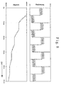
- FIG. 8 shows the course in the upper curve a tuning voltage that is about 1 volt too low. This becomes clear from the cutting off of the overwhelming Minimum amplitudes at the beginning of each vibration block. By gradual lowering of the below also over time shown adjustment voltage will be within a few Milliseconds raised the envelope of the tuning voltage so that they are again in the middle of the intended range lies.
- the Tuning voltage by raising the adjustment voltage one Shift of the tuning voltage in the middle of the given one Limits.
- the invention is not limited in its execution the preferred embodiment given above, a number of variants are conceivable, which ones from that shown in the drawing and description Solution also for fundamentally different types Makes use of.
Landscapes
- Stabilization Of Oscillater, Synchronisation, Frequency Synthesizers (AREA)
- Channel Selection Circuits, Automatic Tuning Circuits (AREA)
Abstract
Description
- Figur 1
- ein Blockschaltbild eines frequenzsteuerbaren Oszillators nach dem Stand der Technik;
- Figur 2
- eine schematische Darstellung einer Oszillator-Frequenzkennlinie;
- Figur 3
- ein Blockschaltbild eines erfindungsgemäß aufgebauten frequenzsteuerbaren Oszillators;
- Figur 4
- ein Blockschaltbild der Verbindung eines Schwellwert-Vergleichers mit einem als Integratormodul ausgebildeten integrierenden Stellglied;
- Figur 5
- ein Blockschaltbild der Verbindung eines Schwellwert-Vergleichers mit einem Analogwert-Speicher als integrierendem Stellglied;
- Figur 6
- eine erste schaltungstechnische Variante eines Frequenzstellgliedes;
- Figur 7
- eine zweite schaltungstechnische Variante eines Frequenzstellgliedes und
- Figur 8
- eine zeitliche Darstellung der (Abstimm-)Steuerspannung und des Abgleichsignals zur Reglung der Ausgangsfrequenz eines Oszillators bei zu geringer Steuerspannung.
Claims (20)
- Verfahren zum Regeln der von einem frequenzsteuerbaren Oszillator abgegebenen Ausgangsfrequenz, deren Abweichung von einer Soll- oder Referenzfrequenz als Abstimmung an den Oszillator abgegeben wird,
dadurch gekennzeichnet,
daß beim Abweichen der Abstimmung von einem vorgegebenen Wert ein den Frequenzbereich der Ausgangsfrequenz bestimmendes Abgleichsignal an den Oszillator abgegeben wird, das den Frequenzbereich in vorgebbaren Zeitabständen, fortlaufend und/oder ereignisgesteuert korrigiert. - Verfahren nach Anspruch 1, dadurch gekennzeichnet, daß das Abgleichsignal den Frequenzbereich so festlegt, daß die der minimalen und der maximalen Ausgangsfrequenz zuzuordnende Abstimmung denselben Abstand von einem mittleren Abstimmungswert aufweist.
- Verfahren nach Anspruch 1 oder 2, dadurch gekennzeichnet, daß das Abgleichsignal den Abgleich des Oszillators (1) schrittweise oder kontinuierlich so korrigiert, daß die Abstimmung nach einer vorgegebenen Zeitspanne innerhalb vorgegebener Grenzwerte liegt.
- Verfahren nach mindestens einem der vorangehenden Ansprüche, dadurch gekennzeichnet, daß die Änderung des Abgleichs innerhalb vorgegebener Zeit- oder Ereignisabschnitte verstärkt oder verringert wird.
- Verfahren nach mindestens einem der vorangehenden Ansprüche, dadurch gekennzeichnet, daß die Änderung des Abgleichs innerhalb vorgegebener Zeit- oder Ereignisabschnitte gesperrt wird.
- Verfahren nach mindestens einem der vorangehenden Ansprüche, dadurch gekennzeichnet, daß die vorgegebenen Grenzwerte der Abstimmung zeit- oder ereignisgesteuert verändert werden.
- Verfahren nach mindestens einem der vorangehenden Ansprüche, dadurch gekennzeichnet, daß die Auswirkung der Grenzwerte der Abstimmung auf die Auslösung gespeicherter Abgleichwerte zeit- oder ereignisgesteuert verändert wird.
- Verfahren nach mindestens einem der vorangehenden Ansprüche, dadurch gekennzeichnet, daß die Auslösung der gespeicherten Abgleichwerte auf Zeitabschnitte kurz nach einem Wechsel der Ausgangsfrequenz begrenzt wird.
- Verfahren nach mindestens einem der vorangehenden Ansprüche, dadurch gekennzeichnet, daß die Auslösung der gespeicherten Abgleichwerte während einer Initialisierungsphase nach dem Einschalten des Oszillators (1) erfolgt.
- Verfahren nach mindestens einem der vorangehenden Ansprüche, dadurch gekennzeichnet, daß nach dem Einschalten des Oszillators (1) definierte Werte des Abstimmsignals an den Oszillator (1) abgegeben werden.
- Verfahren nach mindestens einem der vorangehenden Ansprüche, dadurch gekennzeichnet, daß die Abstimmung des Ozillators (1) mittels Nachlaufsynchronisation (Phase Locked Loop, PLL), Frequenznachführung (Frequency Locked Loop, FLL), direkter digitaler Synthese (DDS) oder digitaler Signalverarbeitung (Digital Signal Processing, DSP) geregelt wird.
- Verfahren nach mindestens einem der vorangehenden Ansprüche, dadurch gekennzeichnet, daß nach dem Einschalten des Oszillators (1) eine Initialisierungsphase eingefügt wird, in der zwischen minimalen und maximalen Werten der Ausgangsfrequenz hin- und hergeschaltet wird und bei einem Über- oder Unterschreiten der unteren und oberen Grenzwerte der Abstimmung der Abgleich des Oszillators (1) so korrigiert wird, daß vorzugsweise nach einer vorgegebenen Zeitspanne der jeweilige Grenzwert nicht mehr über- oder unterschritten wird.
- Frequenzsteuerbarer Oszillator zur Abgabe einer Ausgangsfrequenz innerhalb eines vorgegebenen Frequenzbereichs mit mindestens einem mechanisch oder elektrisch beeinflußbaren Frequenzstellglied zum Einstellen der vom Oszillator abgegebenen Ausgangsfrequenz und mit einer Phasenregelschleife, die ein die Abweichung der Ausgangsfrequenz von einer Soll- oder Referenzfrequenz entsprechendes Abstimmsignal an einen Abstimmeingang des Oszillators abgibt,
dadurch gekennzeichnet,
daß ein mit dem Frequenzstellglied verbundener Abgleicheingang (11) des Oszillators (1) an ein integrierendes Stellglied (6) angeschlossen ist, das über einen Schwellwert-Vergleicher (4) mit dem von der Phasenregelschleife (2) abgegebenen Abstimmwert beaufschlagt ist. - Frequenzsteuerbarer Oszillator nach Anspruch 13, dadurch gekennzeichnet, daß eine Vergleichsspannungs- und Zeitsteuereinrichtung (5) mit dem Schwellwert-Vergleicher (4) und/oder mit dem integrierende Stellglied (6) verbunden ist und den Schwellwert-Vergleicher (4) und/oder das integrierende Stellglied (6) zeit- oder ereignisgesteuert beeinflußt.
- Frequenzsteuerbaren Oszillator nach Anspruch 13 oder 14, dadurch gekennzeichnet, daß der Schwellwert-Vergleicher (4) aus einem Fenster-Diskriminator (3) besteht und daß die Vergleichsspannungs- und Zeitsteuereinrichtung (5) die Grenzwerte des Fenster-Diskriminators (3), die Charakteristik des Fenster-Diskriminators (3) in der Nähe der Grenzwerte und/oder die Intensität des Einflusses des Fenster-Diskriminators (3) auf das integrierende Stellglied (6) beeinflußt.
- Frequenzsteuerbaren Oszillator nach einem der Ansprüche 13 bis 15, dadurch gekennzeichnet, daß der Erfassungseingang des Schwellwert-Vergleichers (4) über einen Tiefpaßfilter (3) mit dem Schleifenfilter (23) der Phasenregelschleife (2) verbunden ist.
- Frequenzsteuerbaren Oszillator nach mindestens einem der vorangehenden Ansprüche 13 bis 16, dadurch gekennzeichnet, daß das integrierende Stellglied (6) aus einem Analogwert-Speicher oder einem Integratormodul besteht, dessen Ausgang mit einem Steueranschluß des Frequenzstellgliedes des Oszillators (1) verbunden ist und daß die Vergleichsspannungs- und Zeitsteuereinrichtung (5) Änderungen des vom Analogwert-Speicher oder Integratormodul abgegebenen Abgleichsignals während vorgegebener Zeit- oder Ereignisabschnitte verstärkt, verringert oder sperrt.
- Frequenzsteuerbaren Oszillator nach Anspruch 17, dadurch gekennzeichnet, daß der Analogwert-Speicher aus der Reihenschaltung eines Aufwärts/Abwärts-Zählers (61), eines Speichers (62) und eines Digital/Analog-Wandlers (63) besteht, daß der Aufwärts-Zähleingang des Aufwärts/Abwärts-Zählers (61) mit dem einen Ausgang des Schwellwert-Vergleichers (4) verbunden ist, der das Überschreiten eines maximalen Grenzwertes angibt und der Abwärts-Zähleingang des Aufwärts/Abwärts-Zählers (61) mit dem anderen Ausgang des Schwellwert-Vergleichers (4) verbunden ist, der das Unterschreiten eines minimalen Grenzwertes anzeigt und daß der Ausgang des Aufwärts/Abwärts-Zählers (61) die Adresse des Lesespeichers (62) ansteuert, die einen unter dieser Adresse gespeicherten Wert an den Digital/Analog-Wandler (63) abgibt, der das Frequenzstellglied des Oszillators (1) ansteuert.
- Frequenzsteuerbaren Oszillator nach mindestens einem der vorangehenden Ansprüche 13 bis 18, dadurch gekennzeichnet, daß das Frequenzstellglied aus einer Spule (12) mit einstellbarer Induktivität, der eine Kapazitätsdiode (13) und ein in seiner Kapazität steuerbarer (Trimm-) Kondensator (14) parallelgeschaltet sind, besteht und daß die Abstimmung mit der Kapazitätsdiode (13) einstellbar ist und der Abgleich mit dem Trimm-Kondensator (14) veränder- bzw. nachregelbar ist.
- Frequenzsteuerbaren Oszillator nach mindestens einem der vorangehenden Ansprüche 13 bis 18, dadurch gekennzeichnet, daß das Frequenzstellglied aus der Parallelschaltung einer Spule (15) mit der Reihenschaltung eines ersten Kondensators (16), einer Kapazitätsdiode (17) und eines zweiten Kondensators (18) besteht, und daß an die Verbindung zwischen dem ersten Kondensator (16) und der Kathode der Kapazitätsdiode (17) über einen ersten Widerstand (19a) die Abgleichspannung und an die Verbindung der Anode der Kapazitätsdiode (17) mit dem zweiten Kondensator (18) über eine Widerstandskombination (19b, 19c) die Abstimmspannung angelegt ist.
Applications Claiming Priority (2)
| Application Number | Priority Date | Filing Date | Title |
|---|---|---|---|
| DE19959265 | 1999-12-03 | ||
| DE19959265A DE19959265A1 (de) | 1999-12-03 | 1999-12-03 | Verfahren zum Regeln der von einem frequenzsteuerbaren Oszillator abgegebenen Ausgangsfrequenz |
Publications (3)
| Publication Number | Publication Date |
|---|---|
| EP1107456A2 true EP1107456A2 (de) | 2001-06-13 |
| EP1107456A3 EP1107456A3 (de) | 2004-01-21 |
| EP1107456B1 EP1107456B1 (de) | 2007-01-03 |
Family
ID=7931920
Family Applications (1)
| Application Number | Title | Priority Date | Filing Date |
|---|---|---|---|
| EP00124958A Expired - Lifetime EP1107456B1 (de) | 1999-12-03 | 2000-11-16 | Verfahren zum Regeln der von einem frequenzsteuerbaren Oszillator abgegebenen Ausgangsfrequenz |
Country Status (5)
| Country | Link |
|---|---|
| EP (1) | EP1107456B1 (de) |
| AT (1) | ATE350811T1 (de) |
| DE (2) | DE19959265A1 (de) |
| DK (1) | DK1107456T3 (de) |
| ES (1) | ES2278570T3 (de) |
Cited By (1)
| Publication number | Priority date | Publication date | Assignee | Title |
|---|---|---|---|---|
| WO2003044961A3 (en) * | 2001-11-16 | 2003-11-27 | Hitachi Ltd | A communication semiconductor integrated circuit device and a wireless communication system |
Families Citing this family (1)
| Publication number | Priority date | Publication date | Assignee | Title |
|---|---|---|---|---|
| DE10240087C5 (de) * | 2002-08-30 | 2011-12-01 | Austriamicrosystems Ag | Vibrationskreisel |
Family Cites Families (9)
| Publication number | Priority date | Publication date | Assignee | Title |
|---|---|---|---|---|
| DE3526363A1 (de) * | 1985-07-19 | 1987-01-22 | Siemens Ag | Verfahren zum herstellen eines einstellbaren frequenzgenerators |
| US4929918A (en) * | 1989-06-07 | 1990-05-29 | International Business Machines Corporation | Setting and dynamically adjusting VCO free-running frequency at system level |
| US5331292A (en) * | 1992-07-16 | 1994-07-19 | National Semiconductor Corporation | Autoranging phase-lock-loop circuit |
| US5382922A (en) * | 1993-12-23 | 1995-01-17 | International Business Machines Corporation | Calibration systems and methods for setting PLL gain characteristics and center frequency |
| DE4415169A1 (de) * | 1994-04-29 | 1995-11-02 | Siemens Ag | Phasenregelkreis |
| DE59702398D1 (de) * | 1996-07-22 | 2000-11-02 | Siemens Ag | Phasenregelkreis mit Technologiekompensation |
| US5736904A (en) * | 1996-12-02 | 1998-04-07 | Motorola, Inc. | Automatic trimming of a controlled oscillator in a phase locked loop |
| US5894246A (en) * | 1997-09-29 | 1999-04-13 | Motorola, Inc. | Automatically tuning a voltage controlled oscillator for minimum side band noise |
| US5942949A (en) * | 1997-10-14 | 1999-08-24 | Lucent Technologies Inc. | Self-calibrating phase-lock loop with auto-trim operations for selecting an appropriate oscillator operating curve |
-
1999
- 1999-12-03 DE DE19959265A patent/DE19959265A1/de not_active Ceased
-
2000
- 2000-11-16 DE DE50013929T patent/DE50013929D1/de not_active Expired - Fee Related
- 2000-11-16 ES ES00124958T patent/ES2278570T3/es not_active Expired - Lifetime
- 2000-11-16 EP EP00124958A patent/EP1107456B1/de not_active Expired - Lifetime
- 2000-11-16 AT AT00124958T patent/ATE350811T1/de not_active IP Right Cessation
- 2000-11-16 DK DK00124958T patent/DK1107456T3/da active
Cited By (3)
| Publication number | Priority date | Publication date | Assignee | Title |
|---|---|---|---|---|
| WO2003044961A3 (en) * | 2001-11-16 | 2003-11-27 | Hitachi Ltd | A communication semiconductor integrated circuit device and a wireless communication system |
| US7148764B2 (en) | 2001-11-16 | 2006-12-12 | Renesas Technology Corp. | Communication semiconductor integrated circuit device and a wireless communication system |
| US7504903B2 (en) | 2001-11-16 | 2009-03-17 | Renesas Technology Corp. | Communication semiconductor integrated circuit device and a wireless communication system |
Also Published As
| Publication number | Publication date |
|---|---|
| ATE350811T1 (de) | 2007-01-15 |
| EP1107456A3 (de) | 2004-01-21 |
| EP1107456B1 (de) | 2007-01-03 |
| ES2278570T3 (es) | 2007-08-16 |
| DE19959265A1 (de) | 2001-06-07 |
| DK1107456T3 (da) | 2007-04-23 |
| DE50013929D1 (de) | 2007-02-15 |
Similar Documents
| Publication | Publication Date | Title |
|---|---|---|
| EP0786708B1 (de) | Fuzzy-Regler bzw. Verfahren zum Abstimmen der Reglerparameter eines Reglers sowie Regler und Verfahren zum Regeln einer Regelstrecke | |
| DE10134640A1 (de) | PLL-Schaltung und Verfahren zur automatischen Einstellung ihrer Ausgangsfrequenz | |
| DE2706224C2 (de) | Digital einstellbarer Frequenzgenerator | |
| DE1959162C3 (de) | Stufenweise nach einem Frequenzraster einstellbarer Frequenzgenerator | |
| DE3202733C2 (de) | ||
| DE69824114T2 (de) | Phasenregelkreis und Verfahren zum Steuern des Phasenregelkreises | |
| DE69030276T2 (de) | Frequenzsynthetisierer | |
| EP1107456B1 (de) | Verfahren zum Regeln der von einem frequenzsteuerbaren Oszillator abgegebenen Ausgangsfrequenz | |
| DE102007001148A1 (de) | Phasenregelschleife zum schnellen Einregeln und darauf bezogenes Verfahren | |
| EP2088672B1 (de) | Schaltung zum Einstellen einer Impedanz | |
| DE2257783B2 (de) | Spannungsgesteuerter Oszillator sowie Verfahren zur elektrischen Änderung der Frequenz eines elektronischen Oszillators | |
| DE10255145A1 (de) | Schaltungsanordnung zur Phasenregelung und Verfahren zum Betrieb der Schaltungsanordnung | |
| EP2618174A1 (de) | Vorrichtung mit einem spannungsgesteuerten Oszillator und einer Schulungsanodnung zum Ansteuern des Oszillators | |
| DE102004059987B4 (de) | Spannungsgesteuerte Oszillatorschaltung mit analoger und digitaler Ansteuerung und phasenverriegelte Regelschleife mit einer solchen Oszillatorschaltung | |
| EP1386400B1 (de) | Phasenregelschleife | |
| EP1847020B1 (de) | Pll- synthesizer mit verbesserter vco vorabstimmung | |
| DE4031939C2 (de) | ||
| EP1333581A1 (de) | Taktsignalerzeugungseinrichtung | |
| EP1374405B1 (de) | Frequenzregelschleife zur frequenzmodulation | |
| DE2735031C3 (de) | Phasenregelkreis | |
| DE68914218T2 (de) | Spannungskommutierungsregler mit stabiliziertes Gewinn. | |
| DE3006632C2 (de) | ||
| WO2000043849A2 (de) | Elektronischer phasenregelkreis (pll) | |
| EP0309922B1 (de) | Schaltung zur kurzzeitigen Erhöhung einer geregelten Betriebsspannung beim Einschalten und bei Spannungseinbrüchen | |
| DE2354871C3 (de) | Schaltung zum Gewinnen einer Stellgleichspannung für die Phasenregelung eines Oszillators |
Legal Events
| Date | Code | Title | Description |
|---|---|---|---|
| PUAI | Public reference made under article 153(3) epc to a published international application that has entered the european phase |
Free format text: ORIGINAL CODE: 0009012 |
|
| AK | Designated contracting states |
Kind code of ref document: A2 Designated state(s): AT BE CH CY DE DK ES FI FR GB GR IE IT LI LU MC NL PT SE TR |
|
| AX | Request for extension of the european patent |
Free format text: AL;LT;LV;MK;RO;SI |
|
| PUAL | Search report despatched |
Free format text: ORIGINAL CODE: 0009013 |
|
| AK | Designated contracting states |
Kind code of ref document: A3 Designated state(s): AT BE CH CY DE DK ES FI FR GB GR IE IT LI LU MC NL PT SE TR |
|
| AX | Request for extension of the european patent |
Extension state: AL LT LV MK RO SI |
|
| 17P | Request for examination filed |
Effective date: 20040217 |
|
| AKX | Designation fees paid |
Designated state(s): AT BE CH CY DE DK ES FI FR GB GR IE IT LI LU MC NL PT SE TR |
|
| 17Q | First examination report despatched |
Effective date: 20050415 |
|
| RAP1 | Party data changed (applicant data changed or rights of an application transferred) |
Owner name: DETEWE SYSTEMS GMBH |
|
| GRAP | Despatch of communication of intention to grant a patent |
Free format text: ORIGINAL CODE: EPIDOSNIGR1 |
|
| GRAS | Grant fee paid |
Free format text: ORIGINAL CODE: EPIDOSNIGR3 |
|
| GRAA | (expected) grant |
Free format text: ORIGINAL CODE: 0009210 |
|
| AK | Designated contracting states |
Kind code of ref document: B1 Designated state(s): AT BE CH CY DE DK ES FI FR GB GR IE IT LI LU MC NL PT SE TR |
|
| PG25 | Lapsed in a contracting state [announced via postgrant information from national office to epo] |
Ref country code: NL Free format text: LAPSE BECAUSE OF FAILURE TO SUBMIT A TRANSLATION OF THE DESCRIPTION OR TO PAY THE FEE WITHIN THE PRESCRIBED TIME-LIMIT Effective date: 20070103 Ref country code: FI Free format text: LAPSE BECAUSE OF FAILURE TO SUBMIT A TRANSLATION OF THE DESCRIPTION OR TO PAY THE FEE WITHIN THE PRESCRIBED TIME-LIMIT Effective date: 20070103 |
|
| REG | Reference to a national code |
Ref country code: GB Ref legal event code: FG4D Free format text: NOT ENGLISH |
|
| REF | Corresponds to: |
Ref document number: 50013929 Country of ref document: DE Date of ref document: 20070215 Kind code of ref document: P |
|
| REG | Reference to a national code |
Ref country code: SE Ref legal event code: TRGR |
|
| GBT | Gb: translation of ep patent filed (gb section 77(6)(a)/1977) |
Effective date: 20070227 |
|
| RAP2 | Party data changed (patent owner data changed or rights of a patent transferred) |
Owner name: AASTRA DETEWE GMBH |
|
| NLT2 | Nl: modifications (of names), taken from the european patent patent bulletin |
Owner name: AASTRA DETEWE GMBH Effective date: 20070404 |
|
| PG25 | Lapsed in a contracting state [announced via postgrant information from national office to epo] |
Ref country code: PT Free format text: LAPSE BECAUSE OF FAILURE TO SUBMIT A TRANSLATION OF THE DESCRIPTION OR TO PAY THE FEE WITHIN THE PRESCRIBED TIME-LIMIT Effective date: 20070604 |
|
| NLV1 | Nl: lapsed or annulled due to failure to fulfill the requirements of art. 29p and 29m of the patents act | ||
| ET | Fr: translation filed | ||
| REG | Reference to a national code |
Ref country code: ES Ref legal event code: FG2A Ref document number: 2278570 Country of ref document: ES Kind code of ref document: T3 |
|
| PLBE | No opposition filed within time limit |
Free format text: ORIGINAL CODE: 0009261 |
|
| STAA | Information on the status of an ep patent application or granted ep patent |
Free format text: STATUS: NO OPPOSITION FILED WITHIN TIME LIMIT |
|
| 26N | No opposition filed |
Effective date: 20071005 |
|
| PG25 | Lapsed in a contracting state [announced via postgrant information from national office to epo] |
Ref country code: GR Free format text: LAPSE BECAUSE OF FAILURE TO SUBMIT A TRANSLATION OF THE DESCRIPTION OR TO PAY THE FEE WITHIN THE PRESCRIBED TIME-LIMIT Effective date: 20070404 |
|
| BERE | Be: lapsed |
Owner name: DETEWE SYSTEMS G.M.B.H. Effective date: 20071130 |
|
| PG25 | Lapsed in a contracting state [announced via postgrant information from national office to epo] |
Ref country code: MC Free format text: LAPSE BECAUSE OF NON-PAYMENT OF DUE FEES Effective date: 20071130 |
|
| REG | Reference to a national code |
Ref country code: DK Ref legal event code: EBP |
|
| EUG | Se: european patent has lapsed | ||
| PG25 | Lapsed in a contracting state [announced via postgrant information from national office to epo] |
Ref country code: BE Free format text: LAPSE BECAUSE OF NON-PAYMENT OF DUE FEES Effective date: 20071130 |
|
| PG25 | Lapsed in a contracting state [announced via postgrant information from national office to epo] |
Ref country code: IE Free format text: LAPSE BECAUSE OF NON-PAYMENT OF DUE FEES Effective date: 20071116 Ref country code: SE Free format text: LAPSE BECAUSE OF NON-PAYMENT OF DUE FEES Effective date: 20071117 Ref country code: DK Free format text: LAPSE BECAUSE OF NON-PAYMENT OF DUE FEES Effective date: 20071130 |
|
| PGFP | Annual fee paid to national office [announced via postgrant information from national office to epo] |
Ref country code: CH Payment date: 20081124 Year of fee payment: 9 |
|
| REG | Reference to a national code |
Ref country code: ES Ref legal event code: FD2A Effective date: 20071117 |
|
| PG25 | Lapsed in a contracting state [announced via postgrant information from national office to epo] |
Ref country code: AT Free format text: LAPSE BECAUSE OF NON-PAYMENT OF DUE FEES Effective date: 20071116 |
|
| PGFP | Annual fee paid to national office [announced via postgrant information from national office to epo] |
Ref country code: IT Payment date: 20081125 Year of fee payment: 9 |
|
| PG25 | Lapsed in a contracting state [announced via postgrant information from national office to epo] |
Ref country code: ES Free format text: LAPSE BECAUSE OF NON-PAYMENT OF DUE FEES Effective date: 20071117 |
|
| PGFP | Annual fee paid to national office [announced via postgrant information from national office to epo] |
Ref country code: FR Payment date: 20081118 Year of fee payment: 9 |
|
| PGFP | Annual fee paid to national office [announced via postgrant information from national office to epo] |
Ref country code: DE Payment date: 20090128 Year of fee payment: 9 |
|
| PGFP | Annual fee paid to national office [announced via postgrant information from national office to epo] |
Ref country code: GB Payment date: 20081121 Year of fee payment: 9 |
|
| PG25 | Lapsed in a contracting state [announced via postgrant information from national office to epo] |
Ref country code: CY Free format text: LAPSE BECAUSE OF FAILURE TO SUBMIT A TRANSLATION OF THE DESCRIPTION OR TO PAY THE FEE WITHIN THE PRESCRIBED TIME-LIMIT Effective date: 20070103 |
|
| PG25 | Lapsed in a contracting state [announced via postgrant information from national office to epo] |
Ref country code: LU Free format text: LAPSE BECAUSE OF NON-PAYMENT OF DUE FEES Effective date: 20071116 |
|
| PG25 | Lapsed in a contracting state [announced via postgrant information from national office to epo] |
Ref country code: TR Free format text: LAPSE BECAUSE OF FAILURE TO SUBMIT A TRANSLATION OF THE DESCRIPTION OR TO PAY THE FEE WITHIN THE PRESCRIBED TIME-LIMIT Effective date: 20070103 |
|
| REG | Reference to a national code |
Ref country code: CH Ref legal event code: PL |
|
| GBPC | Gb: european patent ceased through non-payment of renewal fee |
Effective date: 20091116 |
|
| REG | Reference to a national code |
Ref country code: FR Ref legal event code: ST Effective date: 20100730 |
|
| PG25 | Lapsed in a contracting state [announced via postgrant information from national office to epo] |
Ref country code: LI Free format text: LAPSE BECAUSE OF NON-PAYMENT OF DUE FEES Effective date: 20091130 Ref country code: CH Free format text: LAPSE BECAUSE OF NON-PAYMENT OF DUE FEES Effective date: 20091130 Ref country code: FR Free format text: LAPSE BECAUSE OF NON-PAYMENT OF DUE FEES Effective date: 20091130 |
|
| PG25 | Lapsed in a contracting state [announced via postgrant information from national office to epo] |
Ref country code: DE Free format text: LAPSE BECAUSE OF NON-PAYMENT OF DUE FEES Effective date: 20100601 |
|
| PG25 | Lapsed in a contracting state [announced via postgrant information from national office to epo] |
Ref country code: GB Free format text: LAPSE BECAUSE OF NON-PAYMENT OF DUE FEES Effective date: 20091116 |
|
| PG25 | Lapsed in a contracting state [announced via postgrant information from national office to epo] |
Ref country code: IT Free format text: LAPSE BECAUSE OF NON-PAYMENT OF DUE FEES Effective date: 20091116 |