EP1109227A2 - Condensateur traversant - Google Patents
Condensateur traversant Download PDFInfo
- Publication number
- EP1109227A2 EP1109227A2 EP00311259A EP00311259A EP1109227A2 EP 1109227 A2 EP1109227 A2 EP 1109227A2 EP 00311259 A EP00311259 A EP 00311259A EP 00311259 A EP00311259 A EP 00311259A EP 1109227 A2 EP1109227 A2 EP 1109227A2
- Authority
- EP
- European Patent Office
- Prior art keywords
- coupled
- feed contact
- operable
- conductive layer
- potential
- Prior art date
- Legal status (The legal status is an assumption and is not a legal conclusion. Google has not performed a legal analysis and makes no representation as to the accuracy of the status listed.)
- Withdrawn
Links
Images


Classifications
-
- H—ELECTRICITY
- H10—SEMICONDUCTOR DEVICES; ELECTRIC SOLID-STATE DEVICES NOT OTHERWISE PROVIDED FOR
- H10D—INORGANIC ELECTRIC SEMICONDUCTOR DEVICES
- H10D89/00—Aspects of integrated devices not covered by groups H10D84/00 - H10D88/00
-
- H—ELECTRICITY
- H10—SEMICONDUCTOR DEVICES; ELECTRIC SOLID-STATE DEVICES NOT OTHERWISE PROVIDED FOR
- H10D—INORGANIC ELECTRIC SEMICONDUCTOR DEVICES
- H10D1/00—Resistors, capacitors or inductors
- H10D1/60—Capacitors
- H10D1/68—Capacitors having no potential barriers
-
- H—ELECTRICITY
- H10—SEMICONDUCTOR DEVICES; ELECTRIC SOLID-STATE DEVICES NOT OTHERWISE PROVIDED FOR
- H10W—GENERIC PACKAGES, INTERCONNECTIONS, CONNECTORS OR OTHER CONSTRUCTIONAL DETAILS OF DEVICES COVERED BY CLASS H10
- H10W20/00—Interconnections in chips, wafers or substrates
- H10W20/40—Interconnections external to wafers or substrates, e.g. back-end-of-line [BEOL] metallisations or vias connecting to gate electrodes
- H10W20/495—Capacitive arrangements or effects of, or between wiring layers
- H10W20/496—Capacitor integral with wiring layers
-
- H—ELECTRICITY
- H10—SEMICONDUCTOR DEVICES; ELECTRIC SOLID-STATE DEVICES NOT OTHERWISE PROVIDED FOR
- H10W—GENERIC PACKAGES, INTERCONNECTIONS, CONNECTORS OR OTHER CONSTRUCTIONAL DETAILS OF DEVICES COVERED BY CLASS H10
- H10W20/00—Interconnections in chips, wafers or substrates
- H10W20/01—Manufacture or treatment
- H10W20/031—Manufacture or treatment of conductive parts of the interconnections
Definitions
- a capacitive structure that uses inter-layer vias to contribute to the overall capacitance of the structure. While vias have been typically used to connect elements in an integrated circuit to a power supply, vias are not typically used in conventional capacitors and have never been used to actually contribute to the capacitance of the device.
- Conventional capacitors typically include two oppositely polarized conductive layers disposed one on top of the other and separated by a dielectric. Due to the typically opposite polarization of the two conductive layers, vias have not been used to connect the conductive layers because using a via to connect the layers would create a short circuit.
- One aspect of the present invention is the use of vias to couple stacked conductive layers and to provide a capacitance not only between adjacent plates in the conductive layers, but also between adjacent vias. This may be provided using a unique charging scheme.
- capacitor 16 comprises alternating conductive layers and via layers.
- a first conductive layer 18 is disposed outwardly from semiconductor substrate 12, and a first via layer 20 is disposed outwardly from first conductive layer 18.
- a second conductive layer 22 is disposed outwardly from first via layer 20 and is coupled to first conductive layer 18 by first via layer 20.
- the term “couple” refers to any direct or indirect electrical connection between two or more elements. The elements said to be “coupled” to one another may or may not physically contact one another.
- First conductive layer 18 is disposed outwardly from semiconductor substrate 12.
- first conductive layer 18 comprises two or more conductive plates, each separated by a dielectric 32.
- the term "plate” may refer to any uniform or nonuniform structure capable of forming a lateral capacitance with an approximately adjacent structure.
- first conductive layer 18 is a feed layer, the plates of first conductive layer 18 comprising a first feed contact 34a and a second feed contact 34b disposed approximately adjacent to first feed contact 34a.
- Feed contacts 34a and 34b are separated by dielectric 32.
- Feed contacts 34 are coupled to a power supply (not explicitly shown), which allows feed contact 34a to be charged with one potential and feed contact 34b with a different potential.
- feed contact 34a is operable to be charged with one potential
- feed contact 34b is operable to be charged with an approximately equal potential of opposite polarity.
- first conductive layer 18 as the feed layer
- the invention is not so limited. Any conductive layer could be coupled to the power supply and serve as a feed layer without departing from the scope of the invention.
- integrated circuit 10 may include multiple feed layers, each coupling selected nodes 30 of capacitor 16 to a particular potential power supply.
- capacitor 16 has two nodes 30a and 30b. Nodes 30a and 30b are separated by dielectric 32. In one aspect of operation, nodes 30a and 30b are operable to be charged with differing potentials, creating a capacitance between feed contacts 34, vias 36, and plates 38 of nodes 30a and 30b. In a particular embodiment, nodes 30a and 30b are operable to be charged with approximately equal magnitude, oppositely polarized charges.
- FIGURE 2 is a cross-sectional view of another exemplary embodiment of a via capacitor 116 constructed in accordance with the teachings of the present invention.
- Capacitor 116 comprises a first conductive layer 118, a first via layer 120, a second conductive layer 122, a second via layer 124, and a third conductive layer 126.
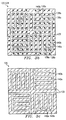
- FIGURES 3a-3c are cut-away views of via capacitor 116 shown in FIGURE 2 along lines 3A-3C, respectively.
- FIGURE 3a is a cut-away view of capacitor 116 along line 3A illustrated in FIGURE 2, showing first conductive layer 118 and first via layer 120.
- fist conductive layer 118 is a feed layer comprising first feed contact 134a and second feed contact 134b.
- first feed contact 134a comprises a plurality of first feed fingers 150
- second feed contact 134b comprises a plurality of second feed fingers 152.
- First feed fingers 150 and second feed fingers 152 are separated by dielectric 132.
- first feed fingers 150 and second feed fingers 152 are interlaced such that each first feed finger 150 is approximately adjacent to at least one second feed finger 152.
- FIGURES 6a-6d have been described as forming plates 38 in second conductive layer 22, similar steps could be implemented to form feed contacts 34 in second conductive layer 22.
Landscapes
- Semiconductor Integrated Circuits (AREA)
- Fixed Capacitors And Capacitor Manufacturing Machines (AREA)
- Internal Circuitry In Semiconductor Integrated Circuit Devices (AREA)
Applications Claiming Priority (2)
| Application Number | Priority Date | Filing Date | Title |
|---|---|---|---|
| US17243999P | 1999-12-17 | 1999-12-17 | |
| US172439P | 1999-12-17 |
Publications (2)
| Publication Number | Publication Date |
|---|---|
| EP1109227A2 true EP1109227A2 (fr) | 2001-06-20 |
| EP1109227A3 EP1109227A3 (fr) | 2004-04-21 |
Family
ID=22627695
Family Applications (1)
| Application Number | Title | Priority Date | Filing Date |
|---|---|---|---|
| EP00311259A Withdrawn EP1109227A3 (fr) | 1999-12-17 | 2000-12-15 | Condensateur traversant |
Country Status (5)
| Country | Link |
|---|---|
| US (1) | US20020072189A1 (fr) |
| EP (1) | EP1109227A3 (fr) |
| JP (1) | JP2001189235A (fr) |
| KR (1) | KR20010062510A (fr) |
| TW (1) | TW499727B (fr) |
Cited By (4)
| Publication number | Priority date | Publication date | Assignee | Title |
|---|---|---|---|---|
| EP1275154A2 (fr) | 2000-04-07 | 2003-01-15 | Koninklijke Philips Electronics N.V. | Structure de condensateur multicouche interdigitee de mos complementaire submicronique profond |
| DE10217566A1 (de) * | 2002-04-19 | 2003-11-13 | Infineon Technologies Ag | Halbleiterbauelement mit integrierter, eine Mehrzahl an Metallisierungsebenen aufweisende Kapazitätsstruktur |
| WO2004075218A1 (fr) * | 2003-02-20 | 2004-09-02 | Infineon Technologies Ag | Condensateur, dispositif a semi-conducteurs a condensateur et procede de fabrication |
| DE102005046734A1 (de) * | 2005-09-29 | 2007-04-05 | Infineon Technologies Ag | Halbleiterbauelement mit integrierter Kapazitätsstruktur |
Families Citing this family (4)
| Publication number | Priority date | Publication date | Assignee | Title |
|---|---|---|---|---|
| KR100425272B1 (ko) * | 2002-05-02 | 2004-03-30 | 주식회사 하이닉스반도체 | 반도체 캐패시터 형성 방법 |
| JP2004172348A (ja) * | 2002-11-20 | 2004-06-17 | Alps Electric Co Ltd | 薄膜コンデンサの形成方法 |
| US20100090308A1 (en) * | 2008-10-10 | 2010-04-15 | Charu Sardana | Metal-oxide-metal capacitors with bar vias |
| US8847376B2 (en) | 2010-07-23 | 2014-09-30 | Tessera, Inc. | Microelectronic elements with post-assembly planarization |
Family Cites Families (6)
| Publication number | Priority date | Publication date | Assignee | Title |
|---|---|---|---|---|
| JP3432963B2 (ja) * | 1995-06-15 | 2003-08-04 | 沖電気工業株式会社 | 半導体集積回路 |
| US5766994A (en) * | 1997-04-11 | 1998-06-16 | Vanguard International Semiconductor Corporation | Dynamic random access memory fabrication method having stacked capacitors with increased capacitance |
| US5770499A (en) * | 1997-05-29 | 1998-06-23 | Texas Instruments Incorporated | Planarized capacitor array structure for high density memory applications |
| US6316801B1 (en) * | 1998-03-04 | 2001-11-13 | Nec Corporation | Semiconductor device having capacitive element structure and multilevel interconnection structure and method of fabricating the same |
| JP3269528B2 (ja) * | 1998-03-04 | 2002-03-25 | 日本電気株式会社 | 容量素子を有する半導体装置及びその製造方法 |
| US6124198A (en) * | 1998-04-22 | 2000-09-26 | Cvc, Inc. | Ultra high-speed chip interconnect using free-space dielectrics |
-
2000
- 2000-12-08 US US09/733,187 patent/US20020072189A1/en not_active Abandoned
- 2000-12-15 EP EP00311259A patent/EP1109227A3/fr not_active Withdrawn
- 2000-12-15 TW TW089126823A patent/TW499727B/zh not_active IP Right Cessation
- 2000-12-16 KR KR1020000077389A patent/KR20010062510A/ko not_active Withdrawn
- 2000-12-18 JP JP2000384106A patent/JP2001189235A/ja active Pending
Cited By (10)
| Publication number | Priority date | Publication date | Assignee | Title |
|---|---|---|---|---|
| EP1275154A2 (fr) | 2000-04-07 | 2003-01-15 | Koninklijke Philips Electronics N.V. | Structure de condensateur multicouche interdigitee de mos complementaire submicronique profond |
| DE10217566A1 (de) * | 2002-04-19 | 2003-11-13 | Infineon Technologies Ag | Halbleiterbauelement mit integrierter, eine Mehrzahl an Metallisierungsebenen aufweisende Kapazitätsstruktur |
| US7061746B2 (en) | 2002-04-19 | 2006-06-13 | Infineon Technologies Ag | Semiconductor component with integrated capacitance structure having a plurality of metallization planes |
| WO2004075218A1 (fr) * | 2003-02-20 | 2004-09-02 | Infineon Technologies Ag | Condensateur, dispositif a semi-conducteurs a condensateur et procede de fabrication |
| US7268383B2 (en) | 2003-02-20 | 2007-09-11 | Infineon Technologies Ag | Capacitor and method of manufacturing a capacitor |
| US7615440B2 (en) | 2003-02-20 | 2009-11-10 | Infineon Technologies Ag | Capacitor and method of manufacturing a capacitor |
| CN1751367B (zh) * | 2003-02-20 | 2010-06-16 | 因芬尼昂技术股份公司 | 电容器及制造电容器的方法 |
| DE102005046734A1 (de) * | 2005-09-29 | 2007-04-05 | Infineon Technologies Ag | Halbleiterbauelement mit integrierter Kapazitätsstruktur |
| US7557426B2 (en) | 2005-09-29 | 2009-07-07 | Infineon Technologies Ag | Integrated capacitor structure |
| DE102005046734B4 (de) * | 2005-09-29 | 2011-06-16 | Infineon Technologies Ag | Halbleiterbauelement mit integrierter Kapazitätsstruktur |
Also Published As
| Publication number | Publication date |
|---|---|
| TW499727B (en) | 2002-08-21 |
| KR20010062510A (ko) | 2001-07-07 |
| EP1109227A3 (fr) | 2004-04-21 |
| JP2001189235A (ja) | 2001-07-10 |
| US20020072189A1 (en) | 2002-06-13 |
Similar Documents
| Publication | Publication Date | Title |
|---|---|---|
| US7274085B1 (en) | Capacitor structure | |
| US5978206A (en) | Stacked-fringe integrated circuit capacitors | |
| KR100815172B1 (ko) | 캐패시터 | |
| US7990676B2 (en) | Density-conforming vertical plate capacitors exhibiting enhanced capacitance and methods of fabricating the same | |
| US5053351A (en) | Method of making stacked E-cell capacitor DRAM cell | |
| US4914546A (en) | Stacked multi-polysilicon layer capacitor | |
| US20070102745A1 (en) | Capacitor structure | |
| JP4621630B2 (ja) | 集積回路用容量性構造およびその製造方法 | |
| US20020047154A1 (en) | Interdigitated multilayer capacitor structure for deep sub-micron CMOS | |
| US11942431B2 (en) | Semiconductor device and manufacturing method thereof | |
| CN100459112C (zh) | 具有集成无源电子组件的电子组件 | |
| CN101390211B (zh) | 三维集成电容结构 | |
| EP1109227A2 (fr) | Condensateur traversant | |
| US6417556B1 (en) | High K dielectric de-coupling capacitor embedded in backend interconnect | |
| US6178083B1 (en) | Layered capacitor device | |
| US7678659B2 (en) | Method of reducing current leakage in a metal insulator metal semiconductor capacitor and semiconductor capacitor thereof | |
| KR102318995B1 (ko) | 트렌치 커패시터 | |
| CN113130444B (zh) | 一种半导体结构及其形成方法 | |
| US20070241425A1 (en) | Three-dimensional capacitor structure | |
| US6600209B1 (en) | Mesh capacitor structure in an integrated circuit | |
| US6323099B1 (en) | High k interconnect de-coupling capacitor with damascene process | |
| EP1943666B1 (fr) | Structure de condensateur | |
| CN100454550C (zh) | 电容结构 | |
| CN1979849A (zh) | 电容结构 | |
| KR100443319B1 (ko) | 반도체 기억장치 및 그 제조방법 |
Legal Events
| Date | Code | Title | Description |
|---|---|---|---|
| PUAI | Public reference made under article 153(3) epc to a published international application that has entered the european phase |
Free format text: ORIGINAL CODE: 0009012 |
|
| AK | Designated contracting states |
Kind code of ref document: A2 Designated state(s): AT BE CH CY DE DK ES FI FR GB GR IE IT LI LU MC NL PT SE TR |
|
| AX | Request for extension of the european patent |
Free format text: AL;LT;LV;MK;RO;SI |
|
| PUAL | Search report despatched |
Free format text: ORIGINAL CODE: 0009013 |
|
| AK | Designated contracting states |
Kind code of ref document: A3 Designated state(s): AT BE CH CY DE DK ES FI FR GB GR IE IT LI LU MC NL PT SE TR |
|
| AX | Request for extension of the european patent |
Extension state: AL LT LV MK RO SI |
|
| AKX | Designation fees paid |
Designated state(s): AT |
|
| REG | Reference to a national code |
Ref country code: DE Ref legal event code: 8566 |
|
| STAA | Information on the status of an ep patent application or granted ep patent |
Free format text: STATUS: THE APPLICATION IS DEEMED TO BE WITHDRAWN |
|
| 18D | Application deemed to be withdrawn |
Effective date: 20041022 |