EP1109432A1 - Wärmeableitung in elektrischem Gerät - Google Patents
Wärmeableitung in elektrischem Gerät Download PDFInfo
- Publication number
- EP1109432A1 EP1109432A1 EP00311330A EP00311330A EP1109432A1 EP 1109432 A1 EP1109432 A1 EP 1109432A1 EP 00311330 A EP00311330 A EP 00311330A EP 00311330 A EP00311330 A EP 00311330A EP 1109432 A1 EP1109432 A1 EP 1109432A1
- Authority
- EP
- European Patent Office
- Prior art keywords
- electrical apparatus
- housing
- platform
- thermally conductive
- component
- Prior art date
- Legal status (The legal status is an assumption and is not a legal conclusion. Google has not performed a legal analysis and makes no representation as to the accuracy of the status listed.)
- Granted
Links
Images

Classifications
-
- H—ELECTRICITY
- H05—ELECTRIC TECHNIQUES NOT OTHERWISE PROVIDED FOR
- H05K—PRINTED CIRCUITS; CASINGS OR CONSTRUCTIONAL DETAILS OF ELECTRIC APPARATUS; MANUFACTURE OF ASSEMBLAGES OF ELECTRICAL COMPONENTS
- H05K7/00—Constructional details common to different types of electric apparatus
- H05K7/20—Modifications to facilitate cooling, ventilating, or heating
- H05K7/2039—Modifications to facilitate cooling, ventilating, or heating characterised by the heat transfer by conduction from the heat generating element to a dissipating body
- H05K7/20436—Inner thermal coupling elements in heat dissipating housings, e.g. protrusions or depressions integrally formed in the housing
-
- H—ELECTRICITY
- H10—SEMICONDUCTOR DEVICES; ELECTRIC SOLID-STATE DEVICES NOT OTHERWISE PROVIDED FOR
- H10W—GENERIC PACKAGES, INTERCONNECTIONS, CONNECTORS OR OTHER CONSTRUCTIONAL DETAILS OF DEVICES COVERED BY CLASS H10
- H10W40/00—Arrangements for thermal protection or thermal control
- H10W40/20—Arrangements for cooling
- H10W40/22—Arrangements for cooling characterised by their shape, e.g. having conical or cylindrical projections
- H10W40/226—Arrangements for cooling characterised by their shape, e.g. having conical or cylindrical projections characterised by projecting parts, e.g. fins to increase surface area
- H10W40/228—Arrangements for cooling characterised by their shape, e.g. having conical or cylindrical projections characterised by projecting parts, e.g. fins to increase surface area the projecting parts being wire-shaped or pin-shaped
Definitions
- the invention which is the subject of this application relates to a device and apparatus for use in the dissipation of heat which is generated by components within electrical apparatus when the apparatus is in operation.
- thermally conductive material is also well known wherein said material is applied to the inside surface of the housing in an attempt to provide some reduction in temperature by using the material to fill in air gaps in the housing but this material is expensive and can add considerably to the cost of the apparatus and as a result use of this form of material is still somewhat limited.
- the aim of the present invention is to allow the use of thermally conductive material to provide an effective cooling effect on components within a housing of electrical apparatus and to do so in an economical manner which minimises the amount of the material which is required to be incorporated while maximising the effect of the same.
- electrical apparatus which comprises at least one electrical or electronic component mounted within a housing, said component mounted on a first side of a printed circuit board and powered by an electricity supply when operational and, when powered, generates heat, said apparatus including thermally conductive material mounted therein to dissipate the heat generated and characterised in that said material is mounted on a raised platform mounted or on or formed by the housing in order to position the material on or adjacent the opposing side of the printed circuit board at the most efficient location to reduce heat with respect to the said component.
- the component is on an upper surface of the printed circuit board and the thermally conductive material is on a lower surface.
- thermally conductive material does not contact the component itself.
- the apparatus will comprise a series of components and if one thermally conductive material position is provided, that position will be determined with respect to design, heat generation and/or efficiency considerations.
- a number of locations can be provided, again, said location determined with reference to the area in which the heat is generated and/or the component locations.
- the housing is formed of sheet material and said sheet material is formed into a platform or platforms at a designated location or locations with respect to the position of components within the housing.
- the platform is formed so as to protrude upwardly from the surface of the housing which in normal use forms the base of the electrical apparatus and this allows the material to be positioned under the component or components at a required distance from the same.
- the sheet material of the housing is sheet metal and the platform which is formed is frustoconical in shape and preferably has a series of slots formed at spaced intervals, said slots allowing two advantages, firstly the reduction in stresses on the sheet material caused by the formation of the platform and secondly the provision of air flow from externally of the housing into the same to improve the cooling effect.
- solder resist material normally coated on a part or whole of the electrical apparatus and/or at least one electrical or electronic component is removed and/or not applied in the area of the thermally conductive material, such that solder is picked up in the area during the solder wave process.
- the extra solder on or surrounding the thermally conductive material increases the thermal conductivity and improves the Electro Magnetic Compatibility (EMC) performance in high current/ high speed regions of the electrical apparatus and/or components.
- EMC Electro Magnetic Compatibility
- the platform can be formed as part of the mould process.
- the thermally conductive material is a gel pad.
- a method of providing a cooling effect on a component or components mounted on an upper surface of a printed circuit board within a housing of electrical apparatus said method including the steps of identifying from tests the heat generated by the components when in operation, identifying the hottest areas within the housing and forming in the housing or locating thereon a platform upon which is mounted thermally conductive sheet material and said platform is of a size so as to position the thermally conductive material at or adjacent the underside of the printed circuit board at or adjacent to the hottest area so as to maximise the cooling effect of the material but without contacting the component or components.
- the provision of the platform allows the use of a minimum of thermally conductive material, preferably provided in a sheet form, to maximum effect as the material can be positioned at the hottest areas in the housing rather than either being placed on the conventional housing inner surface which is removed from the hottest areas or alternatively the sheet material being provided in a relatively thick block to enable the same to reach the hottest areas which is prohibitively expensive.
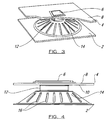
- electrical apparatus which comprises a housing 2 and part of the base of which is shown although it should be appreciated that in practice the housing has a base, a top surface, side walls and front and rear walls.
- a printed circuit board (PCB) 4 on which there are typically provided a series of components which are interconnected to perform the functions of the apparatus but for illustrative purposes only one component 6 in the form of an integrated circuit component is shown.
- the component is mounted on the top side 8 of the board.
- a layer of thermally conductive material 12 which is mounted on a platform 14 to raise the thermally conductive material to a designated height and position with respect to the component 6.
- the platform 14 is, in this embodiment formed as part of the housing base and is formed in a frustoconical shape as shown with a series of slots 16 at spaced intervals around the wall of the same and typically is stamped or pressed as the housing is shaped and formed prior to the assembly with the PCB to form the electrical apparatus.
- the platform or platforms can be formed so as to position the thermally conductive material at or adjacent to the hot spots underneath the printed circuit board.
- the platform 14 is raised to a height of 7mm which leaves a 3mm gap which is filled by the 4mm thick thermally conductive material 12 in the form of a gel pad.
- This pad which is under slight compression acts as a thermal interface between the printed circuit board and the housing.
- the reduction in temperature achieved was found to be 23 degrees Celsius.
- the thermal impedance of the heat path of the PCB is significantly reduced by providing a gel pad and metal dome heatsink. The gel pad does not contact the component directly and only comes into contact with a ground plane of the underside of the PCB.
- the conductive gel pad is typically of a ball grid array type.
- Thermal conductivity/contact between the PCB and the thermally conductive gel pad can be increased by removing solder resist material from the area of the bottom of the PCB adjacent and/or surrounding the pad. During the solder wave process in assembly of the PCB, the area of the PCB not having solder resist picks up solder, thereby reducing the thermal impedance of the heat path in the PCB. This in turn increases the reliability and performance of the PCB and electrical apparatus.
- Removal of solder resist in this area to allow solder to be picked up during the solder wave process results in low thermal resistance from the PCB to the gel pad, both by eliminating the low but finite thermal resistance of i.e., the thin layer of green epoxy resist material, and by providing better contact of the gel pad to the thermal vias and surrounding plane of the PCB. Conduction of heat from the main ground plane of the PCB will also benefit heat dissipation and reduce electrical noise.
- Trailing edges of the components of the PCB can be tapered to also assist in controlled solder thickness on the PCB, thereby avoiding "blobbing" of the solder.
- the invention is equally applicable if placed to the top of the printed circuit board to allow the same to be cooled at the top of the component so that heat is dissipated through the upper surface of the component.
- the present invention provides a means of reducing the internal temperature of an integrated circuit by transferring heat via the gel pad and dissipating the heat into the housing of the apparatus surrounding the integrated circuit.
Landscapes
- Physics & Mathematics (AREA)
- Thermal Sciences (AREA)
- Engineering & Computer Science (AREA)
- Microelectronics & Electronic Packaging (AREA)
- Cooling Or The Like Of Electrical Apparatus (AREA)
- Heating, Cooling, Or Curing Plastics Or The Like In General (AREA)
- Cooling Or The Like Of Semiconductors Or Solid State Devices (AREA)
Applications Claiming Priority (2)
| Application Number | Priority Date | Filing Date | Title |
|---|---|---|---|
| GBGB9929800.2A GB9929800D0 (en) | 1999-12-17 | 1999-12-17 | Heat dissipation in electrical apparatus |
| GB9929800 | 1999-12-17 |
Publications (2)
| Publication Number | Publication Date |
|---|---|
| EP1109432A1 true EP1109432A1 (de) | 2001-06-20 |
| EP1109432B1 EP1109432B1 (de) | 2004-04-21 |
Family
ID=10866473
Family Applications (1)
| Application Number | Title | Priority Date | Filing Date |
|---|---|---|---|
| EP00311330A Expired - Lifetime EP1109432B1 (de) | 1999-12-17 | 2000-12-18 | Wärmeableitung in elektrischem Gerät |
Country Status (5)
| Country | Link |
|---|---|
| US (1) | US6498726B2 (de) |
| EP (1) | EP1109432B1 (de) |
| AT (1) | ATE265132T1 (de) |
| DE (1) | DE60010025T2 (de) |
| GB (1) | GB9929800D0 (de) |
Cited By (5)
| Publication number | Priority date | Publication date | Assignee | Title |
|---|---|---|---|---|
| WO2003056893A1 (es) * | 2001-12-27 | 2003-07-10 | Lear Automotive (Eeds) Spain, S.L. | Contenedor electrónico integrado |
| DE10246577A1 (de) * | 2002-10-05 | 2004-04-15 | Hella Kg Hueck & Co. | Leiterplatte mit Metallgehäuse |
| WO2013167227A3 (de) * | 2012-05-08 | 2014-04-10 | Sew-Eurodrive Gmbh & Co. Kg | Elektrogerät mit gehäuseteil |
| CN104655683A (zh) * | 2015-03-06 | 2015-05-27 | 金陵科技学院 | 能够降温的检测便携装置 |
| DE102015213164A1 (de) * | 2015-07-14 | 2017-01-19 | Conti Temic Microelectronic Gmbh | Leistungselektronikanordnung, Wechselrichter mit einer Leistungselektronikanordnung |
Families Citing this family (11)
| Publication number | Priority date | Publication date | Assignee | Title |
|---|---|---|---|---|
| US20030210524A1 (en) * | 2002-03-13 | 2003-11-13 | Henry Berg | Computer assembly for facilitating heat dissipation |
| JP2003289191A (ja) * | 2002-03-28 | 2003-10-10 | Denso Corp | 電子制御装置 |
| US6700782B1 (en) * | 2002-11-27 | 2004-03-02 | Intel Corporation | Apparatus and method to retain an electronic component in a precise position during assembly manufacturing |
| TW556475B (en) * | 2003-02-19 | 2003-10-01 | Accton Technology Corp | A cover apparatus for dissipating heat and shielding electromagnetic interference |
| US7481267B2 (en) * | 2003-06-26 | 2009-01-27 | The Regents Of The University Of California | Anisotropic thermal and electrical applications of composites of ceramics and carbon nanotubes |
| US6976532B2 (en) * | 2003-06-26 | 2005-12-20 | The Regents Of The University Of California | Anisotropic thermal applications of composites of ceramics and carbon nanotubes |
| US6898084B2 (en) * | 2003-07-17 | 2005-05-24 | The Bergquist Company | Thermal diffusion apparatus |
| US7760507B2 (en) * | 2007-12-26 | 2010-07-20 | The Bergquist Company | Thermally and electrically conductive interconnect structures |
| JP2011077578A (ja) * | 2009-09-29 | 2011-04-14 | Mitsumi Electric Co Ltd | チューナモジュール |
| DE102015218937A1 (de) | 2015-09-30 | 2017-03-30 | Continental Teves Ag & Co. Ohg | Elektronischer Schaltungsträger, Kühlkörper und elektrische Vorrichtung |
| CN116124298B (zh) * | 2021-11-12 | 2026-04-14 | 北京振兴计量测试研究所 | 一种冷却结构和设计方法 |
Citations (6)
| Publication number | Priority date | Publication date | Assignee | Title |
|---|---|---|---|---|
| US4924352A (en) * | 1987-12-22 | 1990-05-08 | Societe Anonyme Dite: Alcatel Cit | Method and device for cooling an integrated circuit package |
| US5307236A (en) * | 1991-07-23 | 1994-04-26 | Alcatel Telspace | Heatsink for contact with multiple electronic components mounted on a circuit board |
| WO1996023397A1 (en) * | 1995-01-25 | 1996-08-01 | Northern Telecom Limited | Printed circuit board and heat sink arrangement |
| US5673176A (en) * | 1995-12-06 | 1997-09-30 | Dell Usa, L.P. | Integrated circuit dual cooling paths and method for constructing same |
| EP0854666A2 (de) * | 1997-01-20 | 1998-07-22 | Robert Bosch Gmbh | Steuergerät bestehend aus mindestens zwei Gehäuseteilen |
| US5991155A (en) * | 1996-12-13 | 1999-11-23 | Mitsubishi Denki Kabushiki Kaisha | Heat sink assembly including flexible heat spreader sheet |
Family Cites Families (5)
| Publication number | Priority date | Publication date | Assignee | Title |
|---|---|---|---|---|
| JP3017837B2 (ja) * | 1991-05-31 | 2000-03-13 | 株式会社日立製作所 | 電子機器装置 |
| US5467251A (en) * | 1993-10-08 | 1995-11-14 | Northern Telecom Limited | Printed circuit boards and heat sink structures |
| JP3597368B2 (ja) * | 1998-02-16 | 2004-12-08 | アルプス電気株式会社 | 電子機器 |
| JP3722616B2 (ja) * | 1998-03-09 | 2005-11-30 | 松下電器産業株式会社 | 情報端末機器 |
| US6156980A (en) * | 1998-06-04 | 2000-12-05 | Delco Electronics Corp. | Flip chip on circuit board with enhanced heat dissipation and method therefor |
-
1999
- 1999-12-17 GB GBGB9929800.2A patent/GB9929800D0/en not_active Ceased
-
2000
- 2000-12-14 US US09/737,203 patent/US6498726B2/en not_active Expired - Lifetime
- 2000-12-18 AT AT00311330T patent/ATE265132T1/de not_active IP Right Cessation
- 2000-12-18 EP EP00311330A patent/EP1109432B1/de not_active Expired - Lifetime
- 2000-12-18 DE DE60010025T patent/DE60010025T2/de not_active Expired - Lifetime
Patent Citations (6)
| Publication number | Priority date | Publication date | Assignee | Title |
|---|---|---|---|---|
| US4924352A (en) * | 1987-12-22 | 1990-05-08 | Societe Anonyme Dite: Alcatel Cit | Method and device for cooling an integrated circuit package |
| US5307236A (en) * | 1991-07-23 | 1994-04-26 | Alcatel Telspace | Heatsink for contact with multiple electronic components mounted on a circuit board |
| WO1996023397A1 (en) * | 1995-01-25 | 1996-08-01 | Northern Telecom Limited | Printed circuit board and heat sink arrangement |
| US5673176A (en) * | 1995-12-06 | 1997-09-30 | Dell Usa, L.P. | Integrated circuit dual cooling paths and method for constructing same |
| US5991155A (en) * | 1996-12-13 | 1999-11-23 | Mitsubishi Denki Kabushiki Kaisha | Heat sink assembly including flexible heat spreader sheet |
| EP0854666A2 (de) * | 1997-01-20 | 1998-07-22 | Robert Bosch Gmbh | Steuergerät bestehend aus mindestens zwei Gehäuseteilen |
Cited By (6)
| Publication number | Priority date | Publication date | Assignee | Title |
|---|---|---|---|---|
| WO2003056893A1 (es) * | 2001-12-27 | 2003-07-10 | Lear Automotive (Eeds) Spain, S.L. | Contenedor electrónico integrado |
| DE10246577A1 (de) * | 2002-10-05 | 2004-04-15 | Hella Kg Hueck & Co. | Leiterplatte mit Metallgehäuse |
| WO2013167227A3 (de) * | 2012-05-08 | 2014-04-10 | Sew-Eurodrive Gmbh & Co. Kg | Elektrogerät mit gehäuseteil |
| CN104655683A (zh) * | 2015-03-06 | 2015-05-27 | 金陵科技学院 | 能够降温的检测便携装置 |
| CN104655683B (zh) * | 2015-03-06 | 2017-11-21 | 金陵科技学院 | 能够降温的检测便携装置 |
| DE102015213164A1 (de) * | 2015-07-14 | 2017-01-19 | Conti Temic Microelectronic Gmbh | Leistungselektronikanordnung, Wechselrichter mit einer Leistungselektronikanordnung |
Also Published As
| Publication number | Publication date |
|---|---|
| DE60010025D1 (de) | 2004-05-27 |
| ATE265132T1 (de) | 2004-05-15 |
| US6498726B2 (en) | 2002-12-24 |
| GB9929800D0 (en) | 2000-02-09 |
| EP1109432B1 (de) | 2004-04-21 |
| DE60010025T2 (de) | 2005-03-31 |
| US20010008481A1 (en) | 2001-07-19 |
Similar Documents
| Publication | Publication Date | Title |
|---|---|---|
| EP1109432B1 (de) | Wärmeableitung in elektrischem Gerät | |
| US6712621B2 (en) | Thermally enhanced interposer and method | |
| US6410982B1 (en) | Heatpipesink having integrated heat pipe and heat sink | |
| US6570764B2 (en) | Low thermal resistance interface for attachment of thermal materials to a processor die | |
| US6816378B1 (en) | Stack up assembly | |
| US5825625A (en) | Heat conductive substrate mounted in PC board for transferring heat from IC to heat sink | |
| EP0913861B1 (de) | Wärmeleitendes Substrat, das in einer Öffnung einer PC-Platine pressmontiert ist, um Wärme vom IC zu einer Wärmesenke zu transferieren | |
| US5920458A (en) | Enhanced cooling of a heat dissipating circuit element | |
| JPH10260230A (ja) | 発熱体の冷却装置 | |
| JP4987231B2 (ja) | 熱伝導性基板パッケージ | |
| JPH09213851A (ja) | Icデバイスの放熱方法及び放熱手段 | |
| CN223414077U (zh) | 功率模组封装结构及电子设备 | |
| US6888722B2 (en) | Thermal design for minimizing interface in a multi-site thermal contact condition | |
| JPH10229288A (ja) | 電力半導体装置 | |
| JPH10294580A (ja) | 発熱体の伝熱部品 | |
| US6173883B1 (en) | Method and apparatus for increasing heat transfer that is restricted in thermally isolated pockets of a medium | |
| JP2002151634A (ja) | 基板放熱装置 | |
| CN2701071Y (zh) | 场效电晶体的散热装置 | |
| JPH11145656A (ja) | 回路基板の放熱方法及び回路基板 | |
| CN1571629A (zh) | 用于待冷却元件的电路布局及相应的冷却方法 | |
| JP4078400B2 (ja) | 電子デバイスの放熱システム | |
| JPH06181395A (ja) | 放熱形プリント配線板 | |
| KR20060057952A (ko) | 인쇄회로기판의 방열구조 | |
| JP2001314074A (ja) | 電源装置 | |
| TW200539407A (en) | FET and its heat sink apparatus |
Legal Events
| Date | Code | Title | Description |
|---|---|---|---|
| PUAI | Public reference made under article 153(3) epc to a published international application that has entered the european phase |
Free format text: ORIGINAL CODE: 0009012 |
|
| AK | Designated contracting states |
Kind code of ref document: A1 Designated state(s): AT BE CH CY DE DK ES FI FR GB GR IE IT LI LU MC NL PT SE TR |
|
| AX | Request for extension of the european patent |
Free format text: AL;LT;LV;MK;RO;SI |
|
| 17P | Request for examination filed |
Effective date: 20010521 |
|
| AKX | Designation fees paid |
Free format text: AT BE CH CY DE DK ES FI FR GB GR IE IT LI LU MC NL PT SE TR |
|
| 17Q | First examination report despatched |
Effective date: 20020620 |
|
| GRAP | Despatch of communication of intention to grant a patent |
Free format text: ORIGINAL CODE: EPIDOSNIGR1 |
|
| RAP1 | Party data changed (applicant data changed or rights of an application transferred) |
Owner name: PACE MICRO TECHNOLOGY PLC |
|
| GRAS | Grant fee paid |
Free format text: ORIGINAL CODE: EPIDOSNIGR3 |
|
| GRAA | (expected) grant |
Free format text: ORIGINAL CODE: 0009210 |
|
| RIN1 | Information on inventor provided before grant (corrected) |
Inventor name: FULLER, COLIN Inventor name: WOODHOUSE, DAVID Inventor name: STURGE, DAVID Inventor name: CROSS, STEPHEN Inventor name: BRISTOW, ANTHONY |
|
| AK | Designated contracting states |
Kind code of ref document: B1 Designated state(s): AT BE CH CY DE DK ES FI FR GB GR IE IT LI LU MC NL PT SE TR |
|
| PG25 | Lapsed in a contracting state [announced via postgrant information from national office to epo] |
Ref country code: CH Free format text: LAPSE BECAUSE OF FAILURE TO SUBMIT A TRANSLATION OF THE DESCRIPTION OR TO PAY THE FEE WITHIN THE PRESCRIBED TIME-LIMIT Effective date: 20040421 Ref country code: BE Free format text: LAPSE BECAUSE OF FAILURE TO SUBMIT A TRANSLATION OF THE DESCRIPTION OR TO PAY THE FEE WITHIN THE PRESCRIBED TIME-LIMIT Effective date: 20040421 Ref country code: NL Free format text: LAPSE BECAUSE OF FAILURE TO SUBMIT A TRANSLATION OF THE DESCRIPTION OR TO PAY THE FEE WITHIN THE PRESCRIBED TIME-LIMIT Effective date: 20040421 Ref country code: CY Free format text: LAPSE BECAUSE OF FAILURE TO SUBMIT A TRANSLATION OF THE DESCRIPTION OR TO PAY THE FEE WITHIN THE PRESCRIBED TIME-LIMIT Effective date: 20040421 Ref country code: FI Free format text: LAPSE BECAUSE OF FAILURE TO SUBMIT A TRANSLATION OF THE DESCRIPTION OR TO PAY THE FEE WITHIN THE PRESCRIBED TIME-LIMIT Effective date: 20040421 Ref country code: AT Free format text: LAPSE BECAUSE OF FAILURE TO SUBMIT A TRANSLATION OF THE DESCRIPTION OR TO PAY THE FEE WITHIN THE PRESCRIBED TIME-LIMIT Effective date: 20040421 Ref country code: TR Free format text: LAPSE BECAUSE OF FAILURE TO SUBMIT A TRANSLATION OF THE DESCRIPTION OR TO PAY THE FEE WITHIN THE PRESCRIBED TIME-LIMIT Effective date: 20040421 Ref country code: LI Free format text: LAPSE BECAUSE OF FAILURE TO SUBMIT A TRANSLATION OF THE DESCRIPTION OR TO PAY THE FEE WITHIN THE PRESCRIBED TIME-LIMIT Effective date: 20040421 |
|
| REG | Reference to a national code |
Ref country code: GB Ref legal event code: FG4D |
|
| REG | Reference to a national code |
Ref country code: CH Ref legal event code: EP |
|
| REG | Reference to a national code |
Ref country code: IE Ref legal event code: FG4D |
|
| REF | Corresponds to: |
Ref document number: 60010025 Country of ref document: DE Date of ref document: 20040527 Kind code of ref document: P |
|
| PG25 | Lapsed in a contracting state [announced via postgrant information from national office to epo] |
Ref country code: DK Free format text: LAPSE BECAUSE OF FAILURE TO SUBMIT A TRANSLATION OF THE DESCRIPTION OR TO PAY THE FEE WITHIN THE PRESCRIBED TIME-LIMIT Effective date: 20040721 Ref country code: SE Free format text: LAPSE BECAUSE OF FAILURE TO SUBMIT A TRANSLATION OF THE DESCRIPTION OR TO PAY THE FEE WITHIN THE PRESCRIBED TIME-LIMIT Effective date: 20040721 Ref country code: GR Free format text: LAPSE BECAUSE OF FAILURE TO SUBMIT A TRANSLATION OF THE DESCRIPTION OR TO PAY THE FEE WITHIN THE PRESCRIBED TIME-LIMIT Effective date: 20040721 |
|
| PG25 | Lapsed in a contracting state [announced via postgrant information from national office to epo] |
Ref country code: ES Free format text: LAPSE BECAUSE OF FAILURE TO SUBMIT A TRANSLATION OF THE DESCRIPTION OR TO PAY THE FEE WITHIN THE PRESCRIBED TIME-LIMIT Effective date: 20040801 |
|
| NLV1 | Nl: lapsed or annulled due to failure to fulfill the requirements of art. 29p and 29m of the patents act | ||
| ET | Fr: translation filed | ||
| REG | Reference to a national code |
Ref country code: CH Ref legal event code: PL |
|
| PG25 | Lapsed in a contracting state [announced via postgrant information from national office to epo] |
Ref country code: LU Free format text: LAPSE BECAUSE OF NON-PAYMENT OF DUE FEES Effective date: 20041218 |
|
| PG25 | Lapsed in a contracting state [announced via postgrant information from national office to epo] |
Ref country code: IE Free format text: LAPSE BECAUSE OF NON-PAYMENT OF DUE FEES Effective date: 20041220 |
|
| PG25 | Lapsed in a contracting state [announced via postgrant information from national office to epo] |
Ref country code: MC Free format text: LAPSE BECAUSE OF NON-PAYMENT OF DUE FEES Effective date: 20041231 |
|
| PLBE | No opposition filed within time limit |
Free format text: ORIGINAL CODE: 0009261 |
|
| STAA | Information on the status of an ep patent application or granted ep patent |
Free format text: STATUS: NO OPPOSITION FILED WITHIN TIME LIMIT |
|
| 26N | No opposition filed |
Effective date: 20050124 |
|
| REG | Reference to a national code |
Ref country code: IE Ref legal event code: MM4A |
|
| PG25 | Lapsed in a contracting state [announced via postgrant information from national office to epo] |
Ref country code: PT Free format text: LAPSE BECAUSE OF NON-PAYMENT OF DUE FEES Effective date: 20040921 |
|
| REG | Reference to a national code |
Ref country code: FR Ref legal event code: CD |
|
| REG | Reference to a national code |
Ref country code: DE Ref legal event code: R082 Ref document number: 60010025 Country of ref document: DE Representative=s name: MAI DOERR BESIER EUROPEAN PATENT ATTORNEYS - E, DE Ref country code: DE Ref legal event code: R082 Ref document number: 60010025 Country of ref document: DE Representative=s name: MAI DOERR BESIER PATENTANWAELTE, DE |
|
| REG | Reference to a national code |
Ref country code: FR Ref legal event code: PLFP Year of fee payment: 16 |
|
| REG | Reference to a national code |
Ref country code: FR Ref legal event code: PLFP Year of fee payment: 17 |
|
| REG | Reference to a national code |
Ref country code: FR Ref legal event code: PLFP Year of fee payment: 18 |
|
| PGFP | Annual fee paid to national office [announced via postgrant information from national office to epo] |
Ref country code: FR Payment date: 20191226 Year of fee payment: 20 Ref country code: IT Payment date: 20191219 Year of fee payment: 20 |
|
| PGFP | Annual fee paid to national office [announced via postgrant information from national office to epo] |
Ref country code: DE Payment date: 20191231 Year of fee payment: 20 Ref country code: GB Payment date: 20200102 Year of fee payment: 20 |
|
| REG | Reference to a national code |
Ref country code: DE Ref legal event code: R071 Ref document number: 60010025 Country of ref document: DE |
|
| REG | Reference to a national code |
Ref country code: GB Ref legal event code: PE20 Expiry date: 20201217 |
|
| PG25 | Lapsed in a contracting state [announced via postgrant information from national office to epo] |
Ref country code: GB Free format text: LAPSE BECAUSE OF EXPIRATION OF PROTECTION Effective date: 20201217 |