EP1109741B1 - Verfahren zur herstellung von durchsichtigen, leitfähigen beschichtungen aus nanopartikeln und deren zusammensetzung - Google Patents
Verfahren zur herstellung von durchsichtigen, leitfähigen beschichtungen aus nanopartikeln und deren zusammensetzung Download PDFInfo
- Publication number
- EP1109741B1 EP1109741B1 EP99942253A EP99942253A EP1109741B1 EP 1109741 B1 EP1109741 B1 EP 1109741B1 EP 99942253 A EP99942253 A EP 99942253A EP 99942253 A EP99942253 A EP 99942253A EP 1109741 B1 EP1109741 B1 EP 1109741B1
- Authority
- EP
- European Patent Office
- Prior art keywords
- process according
- film
- forming agent
- film forming
- aqueous dispersion
- Prior art date
- Legal status (The legal status is an assumption and is not a legal conclusion. Google has not performed a legal analysis and makes no representation as to the accuracy of the status listed.)
- Expired - Lifetime
Links
Images

Classifications
-
- C—CHEMISTRY; METALLURGY
- C01—INORGANIC CHEMISTRY
- C01B—NON-METALLIC ELEMENTS; COMPOUNDS THEREOF; METALLOIDS OR COMPOUNDS THEREOF NOT COVERED BY SUBCLASS C01C
- C01B13/00—Oxygen; Ozone; Oxides or hydroxides in general
- C01B13/14—Methods for preparing oxides or hydroxides in general
- C01B13/145—After-treatment of oxides or hydroxides, e.g. pulverising, drying, decreasing the acidity
-
- B—PERFORMING OPERATIONS; TRANSPORTING
- B82—NANOTECHNOLOGY
- B82Y—SPECIFIC USES OR APPLICATIONS OF NANOSTRUCTURES; MEASUREMENT OR ANALYSIS OF NANOSTRUCTURES; MANUFACTURE OR TREATMENT OF NANOSTRUCTURES
- B82Y30/00—Nanotechnology for materials or surface science, e.g. nanocomposites
-
- C—CHEMISTRY; METALLURGY
- C03—GLASS; MINERAL OR SLAG WOOL
- C03C—CHEMICAL COMPOSITION OF GLASSES, GLAZES OR VITREOUS ENAMELS; SURFACE TREATMENT OF GLASS; SURFACE TREATMENT OF FIBRES OR FILAMENTS MADE FROM GLASS, MINERALS OR SLAGS; JOINING GLASS TO GLASS OR OTHER MATERIALS
- C03C17/00—Surface treatment of glass, not in the form of fibres or filaments, by coating
- C03C17/06—Surface treatment of glass, not in the form of fibres or filaments, by coating with metals
- C03C17/10—Surface treatment of glass, not in the form of fibres or filaments, by coating with metals by deposition from the liquid phase
-
- C—CHEMISTRY; METALLURGY
- C03—GLASS; MINERAL OR SLAG WOOL
- C03C—CHEMICAL COMPOSITION OF GLASSES, GLAZES OR VITREOUS ENAMELS; SURFACE TREATMENT OF GLASS; SURFACE TREATMENT OF FIBRES OR FILAMENTS MADE FROM GLASS, MINERALS OR SLAGS; JOINING GLASS TO GLASS OR OTHER MATERIALS
- C03C17/00—Surface treatment of glass, not in the form of fibres or filaments, by coating
- C03C17/22—Surface treatment of glass, not in the form of fibres or filaments, by coating with other inorganic material
- C03C17/23—Oxides
- C03C17/25—Oxides by deposition from the liquid phase
-
- H—ELECTRICITY
- H01—ELECTRIC ELEMENTS
- H01B—CABLES; CONDUCTORS; INSULATORS; SELECTION OF MATERIALS FOR THEIR CONDUCTIVE, INSULATING OR DIELECTRIC PROPERTIES
- H01B1/00—Conductors or conductive bodies characterised by the conductive materials; Selection of materials as conductors
- H01B1/20—Conductive material dispersed in non-conductive organic material
-
- H—ELECTRICITY
- H10—SEMICONDUCTOR DEVICES; ELECTRIC SOLID-STATE DEVICES NOT OTHERWISE PROVIDED FOR
- H10F—INORGANIC SEMICONDUCTOR DEVICES SENSITIVE TO INFRARED RADIATION, LIGHT, ELECTROMAGNETIC RADIATION OF SHORTER WAVELENGTH OR CORPUSCULAR RADIATION
- H10F71/00—Manufacture or treatment of devices covered by this subclass
- H10F71/138—Manufacture of transparent electrodes, e.g. transparent conductive oxides [TCO] or indium tin oxide [ITO] electrodes
-
- C—CHEMISTRY; METALLURGY
- C01—INORGANIC CHEMISTRY
- C01P—INDEXING SCHEME RELATING TO STRUCTURAL AND PHYSICAL ASPECTS OF SOLID INORGANIC COMPOUNDS
- C01P2004/00—Particle morphology
- C01P2004/60—Particles characterised by their size
- C01P2004/64—Nanometer sized, i.e. from 1-100 nanometer
-
- C—CHEMISTRY; METALLURGY
- C01—INORGANIC CHEMISTRY
- C01P—INDEXING SCHEME RELATING TO STRUCTURAL AND PHYSICAL ASPECTS OF SOLID INORGANIC COMPOUNDS
- C01P2006/00—Physical properties of inorganic compounds
- C01P2006/22—Rheological behaviour as dispersion, e.g. viscosity, sedimentation stability
-
- C—CHEMISTRY; METALLURGY
- C01—INORGANIC CHEMISTRY
- C01P—INDEXING SCHEME RELATING TO STRUCTURAL AND PHYSICAL ASPECTS OF SOLID INORGANIC COMPOUNDS
- C01P2006/00—Physical properties of inorganic compounds
- C01P2006/40—Electric properties
-
- C—CHEMISTRY; METALLURGY
- C01—INORGANIC CHEMISTRY
- C01P—INDEXING SCHEME RELATING TO STRUCTURAL AND PHYSICAL ASPECTS OF SOLID INORGANIC COMPOUNDS
- C01P2006/00—Physical properties of inorganic compounds
- C01P2006/60—Optical properties, e.g. expressed in CIELAB-values
-
- C—CHEMISTRY; METALLURGY
- C03—GLASS; MINERAL OR SLAG WOOL
- C03C—CHEMICAL COMPOSITION OF GLASSES, GLAZES OR VITREOUS ENAMELS; SURFACE TREATMENT OF GLASS; SURFACE TREATMENT OF FIBRES OR FILAMENTS MADE FROM GLASS, MINERALS OR SLAGS; JOINING GLASS TO GLASS OR OTHER MATERIALS
- C03C2217/00—Coatings on glass
- C03C2217/20—Materials for coating a single layer on glass
- C03C2217/21—Oxides
- C03C2217/211—SnO2
-
- C—CHEMISTRY; METALLURGY
- C03—GLASS; MINERAL OR SLAG WOOL
- C03C—CHEMICAL COMPOSITION OF GLASSES, GLAZES OR VITREOUS ENAMELS; SURFACE TREATMENT OF GLASS; SURFACE TREATMENT OF FIBRES OR FILAMENTS MADE FROM GLASS, MINERALS OR SLAGS; JOINING GLASS TO GLASS OR OTHER MATERIALS
- C03C2217/00—Coatings on glass
- C03C2217/20—Materials for coating a single layer on glass
- C03C2217/21—Oxides
- C03C2217/217—FeOx, CoOx, NiOx
-
- C—CHEMISTRY; METALLURGY
- C03—GLASS; MINERAL OR SLAG WOOL
- C03C—CHEMICAL COMPOSITION OF GLASSES, GLAZES OR VITREOUS ENAMELS; SURFACE TREATMENT OF GLASS; SURFACE TREATMENT OF FIBRES OR FILAMENTS MADE FROM GLASS, MINERALS OR SLAGS; JOINING GLASS TO GLASS OR OTHER MATERIALS
- C03C2217/00—Coatings on glass
- C03C2217/20—Materials for coating a single layer on glass
- C03C2217/21—Oxides
- C03C2217/23—Mixtures
- C03C2217/231—In2O3/SnO2
-
- C—CHEMISTRY; METALLURGY
- C03—GLASS; MINERAL OR SLAG WOOL
- C03C—CHEMICAL COMPOSITION OF GLASSES, GLAZES OR VITREOUS ENAMELS; SURFACE TREATMENT OF GLASS; SURFACE TREATMENT OF FIBRES OR FILAMENTS MADE FROM GLASS, MINERALS OR SLAGS; JOINING GLASS TO GLASS OR OTHER MATERIALS
- C03C2217/00—Coatings on glass
- C03C2217/20—Materials for coating a single layer on glass
- C03C2217/21—Oxides
- C03C2217/24—Doped oxides
-
- C—CHEMISTRY; METALLURGY
- C03—GLASS; MINERAL OR SLAG WOOL
- C03C—CHEMICAL COMPOSITION OF GLASSES, GLAZES OR VITREOUS ENAMELS; SURFACE TREATMENT OF GLASS; SURFACE TREATMENT OF FIBRES OR FILAMENTS MADE FROM GLASS, MINERALS OR SLAGS; JOINING GLASS TO GLASS OR OTHER MATERIALS
- C03C2217/00—Coatings on glass
- C03C2217/20—Materials for coating a single layer on glass
- C03C2217/25—Metals
- C03C2217/251—Al, Cu, Mg or noble metals
- C03C2217/254—Noble metals
-
- C—CHEMISTRY; METALLURGY
- C03—GLASS; MINERAL OR SLAG WOOL
- C03C—CHEMICAL COMPOSITION OF GLASSES, GLAZES OR VITREOUS ENAMELS; SURFACE TREATMENT OF GLASS; SURFACE TREATMENT OF FIBRES OR FILAMENTS MADE FROM GLASS, MINERALS OR SLAGS; JOINING GLASS TO GLASS OR OTHER MATERIALS
- C03C2218/00—Methods for coating glass
- C03C2218/10—Deposition methods
- C03C2218/11—Deposition methods from solutions or suspensions
-
- Y—GENERAL TAGGING OF NEW TECHNOLOGICAL DEVELOPMENTS; GENERAL TAGGING OF CROSS-SECTIONAL TECHNOLOGIES SPANNING OVER SEVERAL SECTIONS OF THE IPC; TECHNICAL SUBJECTS COVERED BY FORMER USPC CROSS-REFERENCE ART COLLECTIONS [XRACs] AND DIGESTS
- Y02—TECHNOLOGIES OR APPLICATIONS FOR MITIGATION OR ADAPTATION AGAINST CLIMATE CHANGE
- Y02E—REDUCTION OF GREENHOUSE GAS [GHG] EMISSIONS, RELATED TO ENERGY GENERATION, TRANSMISSION OR DISTRIBUTION
- Y02E10/00—Energy generation through renewable energy sources
- Y02E10/50—Photovoltaic [PV] energy
Definitions
- This invention relates generally to a composition for forming transparent, electrically conductive coatings. More particularly, the present invention relates to substantially stable dispersions of nanocrystalline materials that form transparent conductive coatings.
- Transparent conductive coatings are generally characterized by low electrical resistance, a high transmittance of visible light, and good film strength. Such coatings may function to dissipate static charge, reduce electromagnetic radiation, or absorb and/or reflect specific types of radiation. Accordingly, such coatings are used in a wide range of devices, including window materials for solar cells, transparent electrodes, liquid crystal displays, reflective layers in architectural glasses, and microelectronic conductive components.
- conductive is less than 10 5 ⁇ / ⁇ (ohms per square)
- static dissipative is 10 5 - 10 9 ⁇ / ⁇
- antistatic is 10 9 - 10 14 ⁇ / ⁇
- Transparent conductive films are commonly made from an oxide semiconductor of which indium-tin oxide ("ITO"), which is an indium oxide containing a minor amount of tin oxide, is typical.
- ITO indium-tin oxide
- suitable electronic conductors include carbon fibers, metal fibers, metal-coated fibers, and aluminum flakes.
- European Patent Specification No: 0 713 240 discloses a transparent conductor film for electric field shielding.
- the film is formed on a glass substrate and comprises an ITO dispersed silicate layer and an overcoat silicate layer.
- the ITO dispersed silicate layer essentially consists of ultra fine particles of indium tin oxide and a silicate-based glass matrix.
- the silicate layer consists of one or more among ultra fine particles selected from a group of ruthenium dioxide, rhenium trioxide, iridium dioxide, rhodium dioxide, and iridium based pyrochlore and a silicate-based glass matrix.
- ATO antimony tin oxide
- Anti-static materials are typically hygroscopic and function as "ionic conductors" by trapping a thin layer of moisture, which help prevent the accumulation of static charge.
- Such materials include compounds such as quaternary ammonium salts, sulfonates, and fatty acid esters.
- conductive films to substrates, namely (1) a process of sputtering film precursors, (2) a process of chemical vapor deposition ("CVD") of film precursors, and (3) a process of the applying film precursors from dispersion.
- CVD chemical vapor deposition
- the substrate is masked, placed in a vacuum chamber, and the film applied during sputtering.
- CVD processes are similar to sputtering.
- dispersion the techniques of spin coating, dip coating, or spraying may be employed to apply the dispersion to the substrate.
- sol-gel chemistry and mechanical attrition are typically employed.
- Sol-gel materials are organic solvent-based dispersions.
- the dispersion process of applying the film precursor is the generally preferred process of applying a film precursor.
- sol-gel dispersions are problematic, however, in that such dispersions are unstable due to ongoing chemical interactions between particles or sol-gel precursors.
- Dispersion instability leads to relatively short operational lifetimes (shelf-life).
- conventional sol-gel derived dispersions must be shipped frozen or refrigerated using dry ice, other suitable refrigerant, or using some other suitable refrigeration method, in order to reduce the continued reactivity and chemical interactions among the particles forming the dispersion, as described above.
- most dispersions are formulated by adding a complex mixture of principally organic solvents. The formulations have short shelf lives, contain large conductive particles (which negatively affect optical quality), or require high cure temperatures that limit their application.
- the coating composition disclosed herein forms transparent, electrically conductive coatings from nanoparticles.
- the preparation process disclosed herein provides a substantially stable composition suitable for use in forming transparent, electrically conductive films.
- a nanocrystalline material with primary particles of indium tin oxide having a substantially spherical shape, and present in an amount of 1% to 25% by weight of the aqueous dispersion is added to and mixed with water to form the aqueous dispersion.
- a substantially stable aqueous dispersion of nanocrystalline particles, which forms a transparent conductive coating is prepared by the process identified above.
- a process according to the invention for forming a substantially transparent film comprises the steps of:
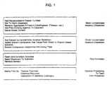
- FIG. 1 there is shown a flow diagram of a process for making conductive transparent films in accordance with one embodiment of the present invention.
- nanocrystalline materials are processed to form transparent conductive ("TC") films.
- TC transparent conductive
- FIG. 1 a flow diagram of a process for preparing aqueous dispersions of nanocrystalline materials for use in forming transparent conductive coatings.
- FIG. 1 a flow diagram of a process for depositing the formulated dispersions of nanocrystalline materials to produce TC films of uniform, controlled thickness, composition, and morphology.
- FIG. 1 is a flow diagram of a process for controlling the characteristics of the deposited nanocrystalline material film to affect film properties.
- the first process step is adding 100% crystalline nanoparticle material (of less than 100 nm with clean defined interfaces) to water.
- acidic or basic aqueous dispersion may be used instead of de-ionized water for acidic or basic nanocrystalline powders, respectively.
- Nanocrystalline material useful in the present invention include, but are not limited to, doped tin oxides, CuO, iron oxides, platinum, palladium, silver and gold.
- the nanoparticulate materials useful in the present composition and process can be discreet primary particles of substantially spherical shape.
- Such nanocrystalline materials, and a process and apparatus for making such nanocrystalline materials are disclosed and claimed in U.S. Patent Nos. 5,874,684, 5,514,349, and 5,460,701.
- Nanosized indium tin oxide is available as an organic-based particulate sol manufactured by dispersing ITO in a solvent, or in a binder solution that comprises a binder polymer dissolved in a mixed organic solvent (a least on polar solvent and at least one non-polar solvent).
- the nanocrystalline particles should be present in an amount at least sufficient to provide an electrically conductive coating when the composition is diluted and applied to a substrate.
- the nanocrystalline particles may be present in amounts ranging from about 1 to about 40 % by weight of the dispersion, most preferably from about 7 to about 30 % by weight of the dispersion.
- the nanocrystalline particles and solvent are then subjected to high shear mixing such as by a mixer emulsifier, or other suitable mixing method, for a time sufficient to form an aqueous dispersion.
- the dispersion is then centrifuged, or clarified of aggregates by other suitable method, the supernatant is collected and filtered, thereby providing a concentrated aqueous metal oxide solution that is relatively free of aggregates.
- a film forming agent is then added to the dispersion.
- the film-forming agents may be polymeric containing at least one hydroxyl group, such as, but not limited to, polyvinyl alcohol-, polyethylene glycol-, or cellulose-based polymers.
- the film forming agent may also be a surfactant, such as but not limited to, organosilanes, ethoxylated alcohols, phosphate esters, glycerol esters, aliphatic polyethers and ethoxylated fatty esters.
- the film forming agent should be present in an amount effective to provide uniform, defect-free films.
- the film-forming agent is preferably added to the dispersion at up to 25% by weight of the nanocrystalline material content. The solids content of the aqueous dispersion may then be adjusted by dilution.
- substantially stable it is meant that the particles do not readily agglomerate, aggregate, or undergo further substantial chemical activity. In other words, there is substantially no latent chemical activity between the nanocrystalline particles.
- the concentrated aqueous dispersion of nanocrystalline particles may be used to make a film by applying the dispersion to a substrate. More particularly, the dispersion is diluted to make a formulation by mixing an appropriate weight percent of a solvent mixture to make the formulation 0.1 to 5 wt% solids.
- the diluent. composition may range from water to organic-based solvents.
- the diluent composition is typically a mixture of low-, medium-, and high-boiling point solvents. Suitable organic diluents include, but are not limited to, alcohols, ketones, and ethers.
- the diluent is mixed with the dispersion by low-shear techniques such as, for example, a paddle blade.
- the diluted aqueous dispersion may then be applied to a cleaned substrate by spin coating, dip coating, meniscus coating, spray coating, or other suitable coating method.
- the method of coating is application specific. For example, a film is applied to a CRT surface by spin coating and a plastic by roll coating. After the dispersion has been applied, the film is heated for a sufficient time to remove the solvent. The drying time will vary depending upon the diluent composition.
- the dried film may be further treated to tailor the electrical and mechanical properties of the film.
- Such treatments include thermal treatment, chemical reduction, and the application of coatings.
- the film is heated to increase the electrical conductivity. More particularly, the film should be heated for a sufficient time at a sufficiently high temperature to cure the particles within the deposited film. Suitable temperatures include a range from about 300°C to about 800°C.
- the deposited film may also be treated by chemical reduction to increase the electrical conductivity.
- Suitable coatings may be applied in a manner similar to that discussed above, for example, by spin coating.
- Suitable coatings include silane monomers or oligomers, such as but not limited to those formed from tetraethoxysilane or tetramethoxysilane, which may then be heated with the film to about 150°C in air or a reducing environment, for a sufficient period of time to dry and cure the films.
- a suitable reducing environment is, for example, a mixture of hydrogen and inert gas (such as, for example, pre-purified nitrogen or argon).
- ITO prepared by physical vapor synthesis (PVS)
- PVS physical vapor synthesis
- a dispersion was prepared in the same manner as set forth in Example 1, except an acidic or basic aqueous solution replaced de-ionized water for acidic or basic nanocrystalline powders, respectively.
- Dispersions were prepared in the manner of Examples 1-2, but film-forming agents were added.
- the film-forming agents may be polymeric containing at least one hydroxyl group, such as, but not limited to, polyvinyl alcohol-, polyethylene glycol- or cellulose-based polymers; or may be a surfactant, such as but not limited to, organosilanes, ethoxylated alcohols, phosphate esters, glycerol esters, aliphatic polyethers and ethoxylated fatty esters.
- the film-forming agent was added to the dispersion at up to about 25 wt% of the metal or metal oxide content.
- the aqueous dispersions in Examples 1-3 were formulated for coating by dilution to an appropriate weight percent with a diluent.
- the diluent composition may range from water to organic-based solvents. Diluent composition determines film drying time and is typically a mixture of low-, medium-, and high-boiling point solvents.
- the ITO formulation prepared in Example 4 was applied to substrates and dried at 120°C for 30 minutes. Films may be further heated to prepare films of controlled conductivity.
- the ITO formulation prepared in Example 4 was applied to substrates and dried at 120°C for 30 minutes.
- the deposited films were subsequently coated with a silane oligomer, such as but not limited to those formed from TEOS or TMOS, and heated to 150°C in air or a reducing environment, such as but not limited to mixtures of hydrogen and inert gas (pre-purified nitrogen or argon), for a period of at least 15 minutes.
- a silane oligomer such as but not limited to those formed from TEOS or TMOS
- the ITO formulation prepared in Example 4 was applied to substrates and heated to between 350°C and 800°C to cure the particles within the deposited film.
- Deposited films were subsequently coated with a silane oligomer, such as but not limited to those formed from TEOS or TMOS, and heated to 150°C in a reducing environment, such as but not limited to mixtures of hydrogen and inert gas (pre-purified nitrogen or argon), for a period of at least 15 minutes.
- a silane oligomer such as but not limited to those formed from TEOS or TMOS
- FIG. 2 is a plot of percent transmission through a film coated on glass as a function of wavelength for a film made in accordance with Example 7. As shown in FIG. 2, the deposited film is characterized by a high degree of transmittance providing an optical transparency of 95%.
- a coating was prepared in the accordance with Examples 6-7, but ITO nanocrystalline powder was replaced or combined with other nanocrystalline formulations containing other metal and metal oxides, such as, but not limited to, doped Tin Oxides, CuO, iron oxides, platinum, palladium, silver and gold.
- Sheet resistance measures 3,000 ⁇ / and is stable at room temperature and 20% relative humidity. Transparency is quantified below. nm 550 650 750 %T 86.1 92.6 96.9
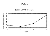
- FIG. 3 is a plot that shows the stability of an aqueous dispersion of ITO prepared in accordance with the method disclosed herein.
- the ITO dispersion is formulated by diluting with the appropriate organic solvents, as discussed in Example 4. This formulation is applied to a substrate and processed, as in Examples 5 and 6.
- the sheet resistance of the film was measured and employed as a method to track the stability of the ITO dispersion. This stability test was done in a humidity chamber, under 80% relative humidity, at 40°C. Such testing accelerates the aging to a rate of approximately 4 to 1, where one day is equivalent to 4. At 12 days, the sheet resistance begins to rise, suggesting that the ITO dispersion has become relatively unstable. It is therefore evident shown that the present ITO dispersion is more stable than known dispersion compositions for transparent conductive coatings, which typically agglomerate within hours at 40°C, 80% relative humidity.
Landscapes
- Chemical & Material Sciences (AREA)
- Engineering & Computer Science (AREA)
- Organic Chemistry (AREA)
- Materials Engineering (AREA)
- Nanotechnology (AREA)
- Geochemistry & Mineralogy (AREA)
- Physics & Mathematics (AREA)
- General Chemical & Material Sciences (AREA)
- Chemical Kinetics & Catalysis (AREA)
- Life Sciences & Earth Sciences (AREA)
- Condensed Matter Physics & Semiconductors (AREA)
- Crystallography & Structural Chemistry (AREA)
- General Physics & Mathematics (AREA)
- Composite Materials (AREA)
- Inorganic Chemistry (AREA)
- Dispersion Chemistry (AREA)
- Spectroscopy & Molecular Physics (AREA)
- Paints Or Removers (AREA)
- Manufacturing Of Electric Cables (AREA)
- Non-Insulated Conductors (AREA)
- Application Of Or Painting With Fluid Materials (AREA)
- Compositions Of Oxide Ceramics (AREA)
- Laminated Bodies (AREA)
- Coating Of Shaped Articles Made Of Macromolecular Substances (AREA)
- Processes Of Treating Macromolecular Substances (AREA)
- Manufacture Of Macromolecular Shaped Articles (AREA)
- Treatments Of Macromolecular Shaped Articles (AREA)
Claims (21)
- Verfahren zur Herstellung einer im Wesentlichen stabilen, wässrigen Dispersion von nanokristallinen Partikeln, die geeignet sind, einer transparenten Beschichtung elektrische Leitfähigkeit zu verleihen, wobei in dem Verfahren ein nanokristallines Material mit Primärpartikeln aus Indiumzinnoxid, die eine im Wesentlichen sphärische Form aufweisen und die in einer Menge von 1 % bis 25 % bezogen auf das Gewicht der wässrigen Dispersion vorhanden sind, in Wasser gegeben und damit gemischt wird, um die wässrige Dispersion zu bilden.
- Verfahren gemäß Anspruch 1, welches den weiteren Schritt des Zugebens eines Filmbildners in einer Menge von bis zu 25 % bezogen auf das Gewicht des nanokristallinen Materials einschließt.
- Verfahren gemäß Anspruch 2, wobei der Filmbildner mindestens eine Hydroxylguppe enthält.
- Verfahren gemäß Anspruch 2, wobei der Filmbildner ein auf Cellulose basierendes Polymer in einer Menge von bis zu 25% bezogen auf das Gewicht des nanokristallinen Materialgehalts umfasst.
- Verfahren gemäß Anspruch 2, wobei der Filmbildner ein auf Cellulose basierendes Polymer in einer Menge von bis zu 5 % bezogen auf das Gewicht des nanokristallinen Materialgehalts umfasst.
- Verfahren gemäß Anspruch 2, wobei der Filmbildner in organischer und wässriger Phase löslich ist.
- Verfahren gemäß Anspruch 2, wobei der Filmbildner in der Dispersion in einer Menge von 5 % bis 15 % bezogen auf das Gewicht des nanokristallinen Materialgehalts vorhanden ist.
- Verfahren gemäß einem der vorstehenden Ansprüche, welches den weiteren Schritt des Zugebens eines Verdünnungsmittels zu der wässrigen Dispersion einschließt.
- Verfahren zur Herstellung eines im Wesentlichen transparenten Films, umfassend die Schritte:(a) Zugeben eines elektrisch leitfähigen, nanokristallinen Materials zu Wasser, wobei das nanokristalline Material Primärpartikel aus Metall oder Metalloxid mit im Wesentlichen sphärischer Form umfasst;(b) Mischen des nanokristallinen Materials und Wasser, um eine elektrisch leitfähige, wässrige Dispersion zu bilden;(c) Zugeben eines Filmbildners zu der wässrigen Dispersion;(d) Zugeben eines Verdünnungsmittels zu der wässrigen Dispersion, um eine Zubereitung herzustellen; und(e) Aufbringen der Zubereitung auf ein Substrat.
- Verfahren gemäß Anspruch 9, wobei der Filmbildner zu der wässrigen Dispersion in einer Menge von bis zu 25 % bezogen auf das Gewicht des nanokristallinen Materials zugegebein wird.
- Verfahren gemäß Anspruch 9, wobei der Filmbildner mindestens eine Hydroxylguppe enthält.
- Verfahren gemäß Anspruch 9, wobei der Filmbildner ein auf Cellulose basierendes Polymer in einer Menge von bis zu 25 % bezogen auf das Gewicht des Metall- oder Metalloxidgehalts umfasst.
- Verfahren gemäß Anspruch 9, umfassend den weiteren Schritt des Zugebens eines Filmbildners zu der wässrigen Dispersion, wobei der Filmbildner ein auf Cellulose basierendes Polymer in einer Menge von bis zu 5 % bezogen auf das Gewicht des Metall- oder Metalloxidgehalts umfasst.
- Verfahren gemäß Anspruch 9, wobei der Filmbildner in organischer und wässriger Phase löslich ist.
- Verfahren gemäß Anspruch 14, wobei der Filmbildner in der Dispersion in einer Menge von 5 % bis 15 % bezogen auf das Gewicht des Metall- oder Metalloxidgehalts vorhanden ist.
- Verfahren gemäß einem der Ansprüche 9 bis 15, welches den weiteren Schritt des Erwärmens des Substrats einschließt, um Wasser und Verdünnungsmittel im Wesentlich zu entfernen, wodurch ein Film auf dem Substrat gebildet wird.
- Verfahren gemäß Anspruch 16, umfassend den weiteren Schritt des Erwärmens des Substrats auf eine Temperatur zwischen 300 °C und 800 °C für eine Zeitdauer, die ausreicht, um die nanokristallinen Partikel im Film zu härten.
- Verfahren gemäß Anspruch 16, umfassend den weiteren Schritt des Beschichtens des Films mit Silanmonomeren oder -oligomeren.
- Verfahren gemäß Anspruch 16, zusätzlich umfassend den Schritt des Erwärmens des Films in einer reduzierenden Umgebung für eine Zeitdauer, die ausreicht, um den Schichtwiderstand des Films zu reduzieren.
- Im Wesentlichen stabile, wässrige Dispersion aus Metalloxidpartikeln, hergestellt durch ein Verfahren gemäß einem der Ansprüche 1 bis 8, die zur Bildung einer transparenten, leitfähigen Beschichtung geeignet ist.
- Im Wesentlichen transparenter Film, hergestellt durch ein Verfahren gemäß einem der Ansprüche 9 bis 19.
Applications Claiming Priority (5)
| Application Number | Priority Date | Filing Date | Title |
|---|---|---|---|
| US9682998P | 1998-08-17 | 1998-08-17 | |
| US96829P | 1998-08-17 | ||
| US374751 | 1999-08-13 | ||
| US09/374,751 US6416818B1 (en) | 1998-08-17 | 1999-08-13 | Compositions for forming transparent conductive nanoparticle coatings and process of preparation therefor |
| PCT/US1999/018677 WO2000009446A1 (en) | 1998-08-17 | 1999-08-16 | Compositions for forming transparent conductive nanoparticle coatings and process of preparation therefor |
Publications (2)
| Publication Number | Publication Date |
|---|---|
| EP1109741A1 EP1109741A1 (de) | 2001-06-27 |
| EP1109741B1 true EP1109741B1 (de) | 2004-10-13 |
Family
ID=26792130
Family Applications (1)
| Application Number | Title | Priority Date | Filing Date |
|---|---|---|---|
| EP99942253A Expired - Lifetime EP1109741B1 (de) | 1998-08-17 | 1999-08-16 | Verfahren zur herstellung von durchsichtigen, leitfähigen beschichtungen aus nanopartikeln und deren zusammensetzung |
Country Status (7)
| Country | Link |
|---|---|
| US (1) | US6416818B1 (de) |
| EP (1) | EP1109741B1 (de) |
| JP (2) | JP2003527454A (de) |
| AU (1) | AU758075B2 (de) |
| CA (1) | CA2340751C (de) |
| DE (1) | DE69921161T2 (de) |
| WO (1) | WO2000009446A1 (de) |
Families Citing this family (90)
| Publication number | Priority date | Publication date | Assignee | Title |
|---|---|---|---|---|
| US6933331B2 (en) * | 1998-05-22 | 2005-08-23 | Nanoproducts Corporation | Nanotechnology for drug delivery, contrast agents and biomedical implants |
| US6497957B1 (en) | 2000-10-04 | 2002-12-24 | Eastman Kodak Company | Antireflection article of manufacture |
| EP1244114A1 (de) * | 2001-03-20 | 2002-09-25 | ILFORD Imaging Switzerland GmbH | Elektrisch aktive Filme |
| JP2003020449A (ja) * | 2001-07-11 | 2003-01-24 | Ishihara Sangyo Kaisha Ltd | 導電性塗料及びそれを用いた導電性塗膜の形成方法 |
| US20030066998A1 (en) * | 2001-08-02 | 2003-04-10 | Lee Howard Wing Hoon | Quantum dots of Group IV semiconductor materials |
| US7005669B1 (en) | 2001-08-02 | 2006-02-28 | Ultradots, Inc. | Quantum dots, nanocomposite materials with quantum dots, devices with quantum dots, and related fabrication methods |
| US6819845B2 (en) * | 2001-08-02 | 2004-11-16 | Ultradots, Inc. | Optical devices with engineered nonlinear nanocomposite materials |
| US6794265B2 (en) * | 2001-08-02 | 2004-09-21 | Ultradots, Inc. | Methods of forming quantum dots of Group IV semiconductor materials |
| US6710366B1 (en) | 2001-08-02 | 2004-03-23 | Ultradots, Inc. | Nanocomposite materials with engineered properties |
| US6855426B2 (en) | 2001-08-08 | 2005-02-15 | Nanoproducts Corporation | Methods for producing composite nanoparticles |
| WO2003020226A2 (en) | 2001-08-31 | 2003-03-13 | L'oreal S.A. | Cosmetic compositions comprising nanoparticles and processes for using the same |
| AU2002366309A1 (en) * | 2001-12-18 | 2003-06-30 | Asahi Kasei Kabushiki Kaisha | Metal oxide dispersion |
| EP1481020A2 (de) * | 2002-02-04 | 2004-12-01 | Nanophase Technologies Corporation | Stabile dispersionen von nanoteilchen in wässrigen medien |
| US7601406B2 (en) * | 2002-06-13 | 2009-10-13 | Cima Nanotech Israel Ltd. | Nano-powder-based coating and ink compositions |
| US7736693B2 (en) * | 2002-06-13 | 2010-06-15 | Cima Nanotech Israel Ltd. | Nano-powder-based coating and ink compositions |
| US7566360B2 (en) * | 2002-06-13 | 2009-07-28 | Cima Nanotech Israel Ltd. | Nano-powder-based coating and ink compositions |
| ATE476470T1 (de) * | 2002-06-28 | 2010-08-15 | Merck Patent Gmbh | Härtung und trocknung von lacksystemen und druckfarben |
| EP1378947A1 (de) * | 2002-07-01 | 2004-01-07 | Interuniversitair Microelektronica Centrum Vzw | Ätzpaste für Halbleiter und Verwendung einer Ätzpaste zum lokalisierten Ätzen von Halbleitersubstraten |
| TWI227719B (en) * | 2002-11-22 | 2005-02-11 | Far Eastern Textile Ltd | Method of preparing a surface modifier for nanoparticles dispersion of inorganic oxide nanoparticles |
| US7708974B2 (en) | 2002-12-10 | 2010-05-04 | Ppg Industries Ohio, Inc. | Tungsten comprising nanomaterials and related nanotechnology |
| US7745514B2 (en) * | 2003-06-24 | 2010-06-29 | Ppg Industries Ohio, Inc. | Tinted, abrasion resistant coating compositions and coated articles |
| US7635727B2 (en) | 2003-06-24 | 2009-12-22 | Ppg Industries Ohio, Inc. | Composite transparencies |
| US7671109B2 (en) | 2003-06-24 | 2010-03-02 | Ppg Industries Ohio, Inc. | Tinted, abrasion resistant coating compositions and coated articles |
| US7612124B2 (en) | 2003-06-24 | 2009-11-03 | Ppg Industries Ohio, Inc. | Ink compositions and related methods |
| US7605194B2 (en) * | 2003-06-24 | 2009-10-20 | Ppg Industries Ohio, Inc. | Aqueous dispersions of polymer-enclosed particles, related coating compositions and coated substrates |
| CA2530122C (en) * | 2003-06-24 | 2010-09-28 | Ppg Industries Ohio, Inc. | Aqueous dispersions of microparticles having a nanoparticulate phase and coating compositions containing the same |
| US20050016061A1 (en) * | 2003-07-21 | 2005-01-27 | Allen Thomas K. | Metal oxide-containing dispersion and method of preparing the same |
| US6913830B2 (en) | 2003-08-14 | 2005-07-05 | Ppg Industries Ohio, Inc. | Coating compositions containing semiconductor colorants |
| WO2005060610A2 (en) * | 2003-12-11 | 2005-07-07 | The Trustees Of Columbia University In The City Ofnew York | Nano-sized particles, processes of making, compositions and uses thereof |
| US20100184911A1 (en) * | 2009-01-22 | 2010-07-22 | Ppg Industries Ohio, Inc. | Aqueous dispersions of polymer-enclosed particles, related coating compositions and coated substrates |
| US7910634B2 (en) * | 2004-03-25 | 2011-03-22 | Ppg Industries Ohio, Inc. | Aqueous dispersions of polymer-enclosed particles, related coating compositions and coated substrates |
| US7081234B1 (en) | 2004-04-05 | 2006-07-25 | Xerox Corporation | Process of making hydrophobic metal oxide nanoparticles |
| KR20070053164A (ko) * | 2004-05-27 | 2007-05-23 | 나노페이스 테크놀로지스 코포레이션 | 나노결정성의 금속산화물 입자, 중합체성 분산제 및표면활성화제들의 조합을 포함하는 증가된 내스크래치성을갖는 물품 |
| EP1810001A4 (de) * | 2004-10-08 | 2008-08-27 | Sdc Materials Llc | Vorrichtung und verfahren zur probenahme und zum sammeln von in einem gasstrom fliessenden pulvern |
| US7265176B2 (en) * | 2005-01-31 | 2007-09-04 | E. I. Du Pont De Nemours And Company | Composition comprising nanoparticle TiO2 and ethylene copolymer |
| JP5009907B2 (ja) * | 2005-06-10 | 2012-08-29 | シーマ ナノ テック イスラエル リミティド | 向上透明導電性被膜及びそれらを作製する方法 |
| US20070015002A1 (en) * | 2005-07-14 | 2007-01-18 | Ut-Battele, Llc | Oxygen-donor and catalytic coatings of metal oxides and metals |
| WO2007011331A2 (en) * | 2005-07-14 | 2007-01-25 | 3M Innovative Properties Company | Water-soluble polymeric substrate having metallic nanoparticle coating |
| SG150516A1 (en) | 2005-08-12 | 2009-03-30 | Cambrios Technologies Corp | Nanowires-based transparent conductors |
| US8178160B2 (en) * | 2006-01-20 | 2012-05-15 | Ppg Industries Ohio, Inc. | Decorative and durable coating having a homogeneous hue, methods for their preparation, and articles coated therewith |
| US20100129524A1 (en) * | 2006-01-20 | 2010-05-27 | Steven Sternberger | Methods of dispensing powder coating compositions and articles coated therewith |
| WO2008085550A2 (en) * | 2006-08-02 | 2008-07-17 | Battelle Memorial Institute | Electrically conductive coating composition |
| US8018568B2 (en) | 2006-10-12 | 2011-09-13 | Cambrios Technologies Corporation | Nanowire-based transparent conductors and applications thereof |
| EP2083865A2 (de) | 2006-10-12 | 2009-08-05 | C-3 International, Llc | Verfahren zur bereitstellung einer prophylaktischen oberflächenbehandlung für flüssigkeitsaufbereitungssysteme und ihre komponenten |
| WO2008046058A2 (en) * | 2006-10-12 | 2008-04-17 | Cambrios Technologies Corporation | Nanowire-based transparent conductors and applications thereof |
| US20090297626A1 (en) * | 2006-11-03 | 2009-12-03 | The Trustees Of Columbia University In The City Of New York | Methods for preparing metal oxides |
| CN101578667B (zh) * | 2007-01-16 | 2011-07-06 | 帝人株式会社 | 透明导电性层压体及其形成的触摸面板 |
| TWI556456B (zh) | 2007-04-20 | 2016-11-01 | 坎畢歐科技公司 | 複合透明導體及形成其之方法 |
| EP2150971B1 (de) | 2007-05-11 | 2018-11-28 | Umicore AG & Co. KG | Verfahren und vorrichtung zur herstellung gleichförmiger und ultrakleiner nanopartikel |
| US20090098289A1 (en) * | 2007-10-12 | 2009-04-16 | Deininger Mark A | Pig and Method for Applying Prophylactic Surface Treatments |
| US8481449B1 (en) | 2007-10-15 | 2013-07-09 | SDCmaterials, Inc. | Method and system for forming plug and play oxide catalysts |
| US20170194515A9 (en) * | 2007-10-17 | 2017-07-06 | Heraeus Precious Metals North America Conshohocken Llc | Dielectric coating for single sided back contact solar cells |
| US8623301B1 (en) | 2008-04-09 | 2014-01-07 | C3 International, Llc | Solid oxide fuel cells, electrolyzers, and sensors, and methods of making and using the same |
| USD627900S1 (en) | 2008-05-07 | 2010-11-23 | SDCmaterials, Inc. | Glove box |
| GB0817224D0 (en) * | 2008-09-19 | 2008-10-29 | Dupont Teijin Films Us Ltd | Coated polymeric substrates |
| US8507050B2 (en) * | 2008-11-12 | 2013-08-13 | Ppg Industries Ohio, Inc. | Methods for depositing ultra thin coatings exhibiting low haze and methods for the preparation of such coatings |
| GB0908300D0 (en) | 2009-05-14 | 2009-06-24 | Dupont Teijin Films Us Ltd | Polyester films |
| US9126191B2 (en) | 2009-12-15 | 2015-09-08 | SDCmaterials, Inc. | Advanced catalysts for automotive applications |
| US8557727B2 (en) | 2009-12-15 | 2013-10-15 | SDCmaterials, Inc. | Method of forming a catalyst with inhibited mobility of nano-active material |
| US8803025B2 (en) | 2009-12-15 | 2014-08-12 | SDCmaterials, Inc. | Non-plugging D.C. plasma gun |
| US9149797B2 (en) | 2009-12-15 | 2015-10-06 | SDCmaterials, Inc. | Catalyst production method and system |
| US8545652B1 (en) | 2009-12-15 | 2013-10-01 | SDCmaterials, Inc. | Impact resistant material |
| US9119309B1 (en) | 2009-12-15 | 2015-08-25 | SDCmaterials, Inc. | In situ oxide removal, dispersal and drying |
| US8652992B2 (en) | 2009-12-15 | 2014-02-18 | SDCmaterials, Inc. | Pinning and affixing nano-active material |
| US8470112B1 (en) | 2009-12-15 | 2013-06-25 | SDCmaterials, Inc. | Workflow for novel composite materials |
| US20130020113A1 (en) * | 2010-01-27 | 2013-01-24 | Javier Jesus Concepcion Corbea | Nanoparticle Electrodes and Methods of Preparation |
| EP2531566B1 (de) * | 2010-02-05 | 2018-09-12 | CAM Holding Corporation | Lichtempfindliche tintenzusammensetzungen und transparente leiter sowie anwendungsverfahren dafür |
| CA2789281C (en) | 2010-02-10 | 2015-11-24 | C3 International, Llc | Low temperature electrolytes for solid oxide cells having high ionic conductivity |
| WO2011140119A2 (en) * | 2010-05-03 | 2011-11-10 | The Regents Of The University Of California | Flexible and moldable materials with bi-conductive surfaces |
| CN102372440B (zh) * | 2010-08-24 | 2013-09-11 | 上海沪正纳米科技有限公司 | 视窗玻璃的隔热防紫外涂抹液 |
| GB201019212D0 (en) | 2010-11-12 | 2010-12-29 | Dupont Teijin Films Us Ltd | Polyester film |
| US8669202B2 (en) | 2011-02-23 | 2014-03-11 | SDCmaterials, Inc. | Wet chemical and plasma methods of forming stable PtPd catalysts |
| US20120298930A1 (en) * | 2011-05-23 | 2012-11-29 | Chaofeng Zou | Nanostructure compositions, coatings, and films |
| JP5352638B2 (ja) * | 2011-07-26 | 2013-11-27 | 石原産業株式会社 | 導電性塗料の製造方法及び該導電性塗料を用いた導電性塗膜の形成方法 |
| CN102432187A (zh) * | 2011-08-11 | 2012-05-02 | 西安交通大学 | 一种在导电玻璃上制备多种形貌金属纳米颗粒薄膜的方法 |
| EP2744590A4 (de) | 2011-08-19 | 2016-03-16 | Sdcmaterials Inc | Beschichtete substrate zur verwendung in der katalyse und katalysatoren sowie verfahren zur beschichtung von substraten mit grundierungszusammensetzungen |
| US9977019B2 (en) * | 2012-04-25 | 2018-05-22 | Ms² Array Llc | Fluorous peptide microarray, detection process using a fluorous peptide microarray, and process of forming a fluorous peptide microarray |
| US9156025B2 (en) | 2012-11-21 | 2015-10-13 | SDCmaterials, Inc. | Three-way catalytic converter using nanoparticles |
| US9511352B2 (en) | 2012-11-21 | 2016-12-06 | SDCmaterials, Inc. | Three-way catalytic converter using nanoparticles |
| WO2015009618A1 (en) | 2013-07-15 | 2015-01-22 | Fcet, Llc | Low temperature solid oxide cells |
| US9586179B2 (en) | 2013-07-25 | 2017-03-07 | SDCmaterials, Inc. | Washcoats and coated substrates for catalytic converters and methods of making and using same |
| US9427732B2 (en) | 2013-10-22 | 2016-08-30 | SDCmaterials, Inc. | Catalyst design for heavy-duty diesel combustion engines |
| JP2016535664A (ja) | 2013-10-22 | 2016-11-17 | エスディーシーマテリアルズ, インコーポレイテッド | リーンNOxトラップの組成物 |
| EP3082171B1 (de) * | 2013-12-09 | 2022-04-27 | Nissan Chemical Corporation | Zusammensetzung für eine anodenpufferschicht einer organische dünnschichtsolarzelle und organische dünnschichtsolarzelle |
| EP3119500A4 (de) | 2014-03-21 | 2017-12-13 | SDC Materials, Inc. | Zusammensetzungen für passive nox-adsorptionssysteme |
| US20180040751A1 (en) | 2015-02-26 | 2018-02-08 | Dynamic Solar Systems Ag | Obtaining a pv film structure by means of a room temperature method and room temperature method for producing a pv film structure |
| JP2018511698A (ja) * | 2015-02-26 | 2018-04-26 | ダイナミック ソーラー システムズ アクツィエンゲゼルシャフトDynamic Solar Systems Ag | 電気工学薄層の製造のための室温方法、その使用、及びこの方法で得られる薄層発熱システム |
| EP3262674A1 (de) * | 2015-02-26 | 2018-01-03 | Dynamic Solar Systems AG | Raumtemperatur-verfahren zur herstellung elektrotechnischer dünnschichten und elektrotechnische dünnschicht |
| WO2016186569A1 (en) * | 2015-05-19 | 2016-11-24 | Ah Eng Siaw | A composition for optimising energy usage |
| WO2016186570A1 (en) * | 2015-05-19 | 2016-11-24 | Ah Eng Siaw | A method of optimising energy usage |
Family Cites Families (17)
| Publication number | Priority date | Publication date | Assignee | Title |
|---|---|---|---|---|
| JPS5785866A (en) | 1980-11-18 | 1982-05-28 | Mitsubishi Metal Corp | Antistatic transparent paint |
| KR840009328A (ko) | 1983-05-27 | 1984-12-26 | 쯔지가다 다께시 | 산화 주석 인듐 졸 조성물 |
| DE3827631A1 (de) | 1988-08-16 | 1990-02-22 | Hoechst Ag | Selbsttragendes flaechengebilde mit wenigstens einer strukturierten oberflaeche |
| DE69223186T2 (de) | 1991-07-24 | 1998-03-12 | Matsushita Electric Ind Co Ltd | Zusammensetzung zur Verwendung in einem transparenten elektrisch leitenden Film sowie Verfahren zur Herstellung dieses Films |
| DE4212633A1 (de) | 1992-04-15 | 1993-10-21 | Inst Neue Mat Gemein Gmbh | Verfahren zur Herstellung oberflächenmodifizierter nanoskaliger keramischer Pulver |
| US5690805A (en) | 1993-05-17 | 1997-11-25 | Electrochemicals Inc. | Direct metallization process |
| JPH06340829A (ja) * | 1993-06-02 | 1994-12-13 | Mitsubishi Materials Corp | 導電膜形成用組成物 |
| US5460701A (en) | 1993-07-27 | 1995-10-24 | Nanophase Technologies Corporation | Method of making nanostructured materials |
| US5504133A (en) | 1993-10-05 | 1996-04-02 | Mitsubishi Materials Corporation | Composition for forming conductive films |
| KR0153029B1 (ko) | 1993-10-28 | 1998-11-16 | 시노자키 아키히코 | 투명 전도성 기판 및 그 제조방법 |
| JP3147644B2 (ja) * | 1994-03-04 | 2001-03-19 | 三菱マテリアル株式会社 | 透明導電膜形成用組成物および透明導電膜 |
| JP2981401B2 (ja) * | 1994-07-15 | 1999-11-22 | 住友大阪セメント株式会社 | 導電性プラスチック板、及び製造方法 |
| JP3230395B2 (ja) * | 1994-11-17 | 2001-11-19 | 三菱マテリアル株式会社 | 導電膜形成用組成物と導電膜の形成方法 |
| EP0713240B1 (de) | 1994-11-17 | 2004-10-13 | Sumitomo Metal Mining Company Limited | Transparente Leiterschicht zur elektrischen Feldabschirmung |
| JPH09193433A (ja) | 1996-01-18 | 1997-07-29 | Rohm Co Ltd | 発熱抵抗体における保護膜 |
| JP3460484B2 (ja) * | 1996-12-25 | 2003-10-27 | 三菱マテリアル株式会社 | 透明導電膜 |
| US5866287A (en) * | 1997-11-13 | 1999-02-02 | Eastman Kodak Company | Imaging element comprising and electrically-conductive layer containing metal antimonate and non-conductive metal-containing colloidal particles |
-
1999
- 1999-08-13 US US09/374,751 patent/US6416818B1/en not_active Expired - Fee Related
- 1999-08-16 CA CA002340751A patent/CA2340751C/en not_active Expired - Fee Related
- 1999-08-16 WO PCT/US1999/018677 patent/WO2000009446A1/en not_active Ceased
- 1999-08-16 AU AU55675/99A patent/AU758075B2/en not_active Ceased
- 1999-08-16 EP EP99942253A patent/EP1109741B1/de not_active Expired - Lifetime
- 1999-08-16 JP JP2000564901A patent/JP2003527454A/ja not_active Withdrawn
- 1999-08-16 DE DE69921161T patent/DE69921161T2/de not_active Expired - Lifetime
-
2008
- 2008-12-10 JP JP2008314223A patent/JP2009131844A/ja active Pending
Also Published As
| Publication number | Publication date |
|---|---|
| JP2003527454A (ja) | 2003-09-16 |
| JP2009131844A (ja) | 2009-06-18 |
| AU758075B2 (en) | 2003-03-13 |
| WO2000009446A8 (en) | 2000-05-25 |
| DE69921161D1 (de) | 2004-11-18 |
| AU5567599A (en) | 2000-03-06 |
| WO2000009446A1 (en) | 2000-02-24 |
| DE69921161T2 (de) | 2005-10-27 |
| EP1109741A1 (de) | 2001-06-27 |
| CA2340751C (en) | 2007-01-09 |
| WO2000009446A9 (en) | 2000-07-13 |
| US6416818B1 (en) | 2002-07-09 |
| CA2340751A1 (en) | 2000-02-24 |
Similar Documents
| Publication | Publication Date | Title |
|---|---|---|
| US6416818B1 (en) | Compositions for forming transparent conductive nanoparticle coatings and process of preparation therefor | |
| CN109206017A (zh) | 一种石墨烯掺杂玻璃镀膜液及其制备方法 | |
| JP3402215B2 (ja) | 導電膜形成用塗布液および導電膜 | |
| DE3735574C2 (de) | ||
| KR100471098B1 (ko) | 열선차폐필름용코팅용액및이를사용하여열선차폐필름을제조하는방법 | |
| CN112174210B (zh) | 水性免分散纳米铯钨氧化物包覆体的制备方法 | |
| US6576290B2 (en) | Method of preparation of an electrically conductive paint | |
| CN105324338B (zh) | 氟掺杂的氧化锡胶体以及用于制备其的方法 | |
| CZ199094A3 (en) | Process for producing electrically conducting layers reflecting infra-red rays on a glass surface, glass ceramics or enamel | |
| JP2003020449A (ja) | 導電性塗料及びそれを用いた導電性塗膜の形成方法 | |
| KR20150088551A (ko) | 알칼리금속산화물이 도핑된 텅스텐산화물 복합체, 투명전도성 조성물, 코팅필름 및 이를 포함하는 광학소자 | |
| KR100378019B1 (ko) | 투명 도전막의 보호막 형성용 조성물 및 이로부터 투명도전막을 제조하는 방법 | |
| JPH0586605B2 (de) | ||
| JP3606772B2 (ja) | 透明帯電防止膜形成用塗料および透明帯電防止膜付基材 | |
| KR20210013705A (ko) | 높은 투명성을 갖는 무기산화물 분산체 | |
| JPH05290621A (ja) | 高 温 焼 成 用 i t o ペ ー ス ト | |
| KR102094581B1 (ko) | 발수성이 우수하고 uv 경화가 가능한 박막용 조성물 및 이로부터 제조된 발수성 박막 | |
| JPH02234309A (ja) | 導電性皮膜形成用組成物 | |
| JPH06279755A (ja) | 電界シールド用処理液 | |
| JP2001139883A (ja) | 透明被膜形成用塗布液、透明被膜付基材および表示装置 | |
| JP2678033B6 (ja) | 塗料材料及びその製法 | |
| JP2000151181A (ja) | 耐食性と抗菌性を有する導電膜とそのための処理液 | |
| JP2008201879A (ja) | 透明帯電防止膜形成用塗料及び透明帯電防止膜並びに透明帯電防止膜の製造方法 | |
| JP2003020420A (ja) | 金微粒子含有塗液及びその製造方法 | |
| JPH11144537A (ja) | 透明導電膜形成方法 |
Legal Events
| Date | Code | Title | Description |
|---|---|---|---|
| PUAI | Public reference made under article 153(3) epc to a published international application that has entered the european phase |
Free format text: ORIGINAL CODE: 0009012 |
|
| 17P | Request for examination filed |
Effective date: 20010212 |
|
| AK | Designated contracting states |
Kind code of ref document: A1 Designated state(s): AT BE CH CY DE DK ES FI FR GB GR IE IT LI LU MC NL PT SE |
|
| AX | Request for extension of the european patent |
Free format text: AL;LT;LV;MK;RO;SI |
|
| 17Q | First examination report despatched |
Effective date: 20010816 |
|
| GRAP | Despatch of communication of intention to grant a patent |
Free format text: ORIGINAL CODE: EPIDOSNIGR1 |
|
| GRAS | Grant fee paid |
Free format text: ORIGINAL CODE: EPIDOSNIGR3 |
|
| GRAA | (expected) grant |
Free format text: ORIGINAL CODE: 0009210 |
|
| AK | Designated contracting states |
Kind code of ref document: B1 Designated state(s): CH DE FR GB LI SE |
|
| PG25 | Lapsed in a contracting state [announced via postgrant information from national office to epo] |
Ref country code: LI Free format text: LAPSE BECAUSE OF FAILURE TO SUBMIT A TRANSLATION OF THE DESCRIPTION OR TO PAY THE FEE WITHIN THE PRESCRIBED TIME-LIMIT Effective date: 20041013 Ref country code: CH Free format text: LAPSE BECAUSE OF FAILURE TO SUBMIT A TRANSLATION OF THE DESCRIPTION OR TO PAY THE FEE WITHIN THE PRESCRIBED TIME-LIMIT Effective date: 20041013 |
|
| REG | Reference to a national code |
Ref country code: GB Ref legal event code: FG4D |
|
| REG | Reference to a national code |
Ref country code: CH Ref legal event code: EP |
|
| REG | Reference to a national code |
Ref country code: IE Ref legal event code: FG4D |
|
| REF | Corresponds to: |
Ref document number: 69921161 Country of ref document: DE Date of ref document: 20041118 Kind code of ref document: P |
|
| PG25 | Lapsed in a contracting state [announced via postgrant information from national office to epo] |
Ref country code: SE Free format text: LAPSE BECAUSE OF FAILURE TO SUBMIT A TRANSLATION OF THE DESCRIPTION OR TO PAY THE FEE WITHIN THE PRESCRIBED TIME-LIMIT Effective date: 20050113 |
|
| LTIE | Lt: invalidation of european patent or patent extension |
Effective date: 20041013 |
|
| REG | Reference to a national code |
Ref country code: CH Ref legal event code: PL |
|
| ET | Fr: translation filed | ||
| PLBI | Opposition filed |
Free format text: ORIGINAL CODE: 0009260 |
|
| PLAX | Notice of opposition and request to file observation + time limit sent |
Free format text: ORIGINAL CODE: EPIDOSNOBS2 |
|
| 26 | Opposition filed |
Opponent name: DEGUSSA AG Effective date: 20050711 |
|
| PLAF | Information modified related to communication of a notice of opposition and request to file observations + time limit |
Free format text: ORIGINAL CODE: EPIDOSCOBS2 |
|
| PLBB | Reply of patent proprietor to notice(s) of opposition received |
Free format text: ORIGINAL CODE: EPIDOSNOBS3 |
|
| PGFP | Annual fee paid to national office [announced via postgrant information from national office to epo] |
Ref country code: GB Payment date: 20110825 Year of fee payment: 13 Ref country code: DE Payment date: 20110830 Year of fee payment: 13 Ref country code: FR Payment date: 20110830 Year of fee payment: 13 |
|
| PLAB | Opposition data, opponent's data or that of the opponent's representative modified |
Free format text: ORIGINAL CODE: 0009299OPPO |
|
| R26 | Opposition filed (corrected) |
Opponent name: EVONIK DEGUSSA GMBH Effective date: 20050711 |
|
| PLCK | Communication despatched that opposition was rejected |
Free format text: ORIGINAL CODE: EPIDOSNREJ1 |
|
| PLBN | Opposition rejected |
Free format text: ORIGINAL CODE: 0009273 |
|
| STAA | Information on the status of an ep patent application or granted ep patent |
Free format text: STATUS: OPPOSITION REJECTED |
|
| 27O | Opposition rejected |
Effective date: 20120628 |
|
| REG | Reference to a national code |
Ref country code: DE Ref legal event code: R100 Ref document number: 69921161 Country of ref document: DE Effective date: 20120628 |
|
| GBPC | Gb: european patent ceased through non-payment of renewal fee |
Effective date: 20120816 |
|
| REG | Reference to a national code |
Ref country code: FR Ref legal event code: ST Effective date: 20130430 |
|
| PG25 | Lapsed in a contracting state [announced via postgrant information from national office to epo] |
Ref country code: GB Free format text: LAPSE BECAUSE OF NON-PAYMENT OF DUE FEES Effective date: 20120816 Ref country code: DE Free format text: LAPSE BECAUSE OF NON-PAYMENT OF DUE FEES Effective date: 20130301 |
|
| PG25 | Lapsed in a contracting state [announced via postgrant information from national office to epo] |
Ref country code: FR Free format text: LAPSE BECAUSE OF NON-PAYMENT OF DUE FEES Effective date: 20120831 |
|
| REG | Reference to a national code |
Ref country code: DE Ref legal event code: R119 Ref document number: 69921161 Country of ref document: DE Effective date: 20130301 |