EP1111356A2 - Verfahren und Vorrichtung zur Behandlung von Halbleitersubstraten - Google Patents
Verfahren und Vorrichtung zur Behandlung von Halbleitersubstraten Download PDFInfo
- Publication number
- EP1111356A2 EP1111356A2 EP00126312A EP00126312A EP1111356A2 EP 1111356 A2 EP1111356 A2 EP 1111356A2 EP 00126312 A EP00126312 A EP 00126312A EP 00126312 A EP00126312 A EP 00126312A EP 1111356 A2 EP1111356 A2 EP 1111356A2
- Authority
- EP
- European Patent Office
- Prior art keywords
- substrate processing
- wavelengths
- plasma
- substrate
- radiation
- Prior art date
- Legal status (The legal status is an assumption and is not a legal conclusion. Google has not performed a legal analysis and makes no representation as to the accuracy of the status listed.)
- Granted
Links
Images




Classifications
-
- H—ELECTRICITY
- H10—SEMICONDUCTOR DEVICES; ELECTRIC SOLID-STATE DEVICES NOT OTHERWISE PROVIDED FOR
- H10P—GENERIC PROCESSES OR APPARATUS FOR THE MANUFACTURE OR TREATMENT OF DEVICES COVERED BY CLASS H10
- H10P50/00—Etching of wafers, substrates or parts of devices
- H10P50/20—Dry etching; Plasma etching; Reactive-ion etching
- H10P50/24—Dry etching; Plasma etching; Reactive-ion etching of semiconductor materials
- H10P50/242—Dry etching; Plasma etching; Reactive-ion etching of semiconductor materials of Group IV materials
-
- H—ELECTRICITY
- H10—SEMICONDUCTOR DEVICES; ELECTRIC SOLID-STATE DEVICES NOT OTHERWISE PROVIDED FOR
- H10P—GENERIC PROCESSES OR APPARATUS FOR THE MANUFACTURE OR TREATMENT OF DEVICES COVERED BY CLASS H10
- H10P74/00—Testing or measuring during manufacture or treatment of wafers, substrates or devices
- H10P74/23—Testing or measuring during manufacture or treatment of wafers, substrates or devices characterised by multiple measurements, corrections, marking or sorting processes
- H10P74/238—Testing or measuring during manufacture or treatment of wafers, substrates or devices characterised by multiple measurements, corrections, marking or sorting processes comprising acting in response to an ongoing measurement without interruption of processing, e.g. endpoint detection or in-situ thickness measurement
-
- H—ELECTRICITY
- H10—SEMICONDUCTOR DEVICES; ELECTRIC SOLID-STATE DEVICES NOT OTHERWISE PROVIDED FOR
- H10P—GENERIC PROCESSES OR APPARATUS FOR THE MANUFACTURE OR TREATMENT OF DEVICES COVERED BY CLASS H10
- H10P74/00—Testing or measuring during manufacture or treatment of wafers, substrates or devices
- H10P74/20—Testing or measuring during manufacture or treatment of wafers, substrates or devices characterised by the properties tested or measured, e.g. structural or electrical properties
- H10P74/203—Structural properties, e.g. testing or measuring thicknesses, line widths, warpage, bond strengths or physical defects
Definitions
- the present invention relates to a technique for monitoring film thickness including a method of controlling etch and deposition processes.
- One specific embodiment of the present invention relates to a method of controlling and detecting the end point in a plasma etch process by using the plasma emission as a broadband light source and measuring the radiation reflected off the wafer being etched with a spectrometer.
- the present invention may be used to control a variety of plasma and non-plasma processes and is particularly useful in controlling plasma etch processes used in the manufacture of integrated circuits.
- Etching one or more layers of a semiconductor substrate in a plasma etch environment is one of the most common steps in the manufacture of integrated circuits.
- Typical plasma etch processes in semiconductor manufacturing are controlled and stopped either as a timed process or by relying on an end point detection (detection of the time at which the film being etched is completely removed) technique that monitors the optical emission lines of certain species in the plasma.
- one common process used to etch a polysilicon gate structure includes three separate steps. The first step removes a top oxide layer that may have formed over the polysilicon, the second step etches the bulk of the polysilicon at a relatively high etch rate to increase wafer throughput and the third step switches to a slower, but more selective (relative to the underlying oxide layer) final etch.
- an endpoint prediction technique that triggers a process switch to obtain high selectivity to the gate oxide near the end of the plasma etch. Because of variations from one etching step to another, a timed etch may result in under- or over-etching of the polysilicon layer.
- employing an endpoint detection technique that monitors optical line emissions relies on exposing the underlayer (i.e., the gate oxide in this example) to the plasma etch chemistry. Such exposure can degrade the integrity of the gate oxide layer.
- an endpoint prediction technique that directly monitors the wafer state is required.
- IEP interferometric endpoint
- the IEP system uses a mercury (Hg) lamp that generates a strong Hg atomic line emission that is coupled to a bifurcated optical fiber.
- a collimating lens and folding mirror set at the output end of the fiber illuminates a spot diameter of approximately 1 cm in diameter on the wafer through a sapphire window mounted on the top of the dome.
- the light reflected from the wafer is coupled back to the second arm of the bifurcated fiber and measured by a single wavelength optical detector, such as a photomultiplier or photodiode.
- the single wavelength optical signal shows optical fringes as the thickness of the top layer film is etched away.
- fringe counting can be used for etch rate measurements and etch-to-depth prediction.
- some films have higher absorption and the fringes will be observed only below a certain film thickness.
- the single wavelength detection limits the IEP system to the existing Hg lines, usually the useful lines are 254, 313, 365, 405 and 435 nm.
- UV ultraviolet
- film properties such as spectral dependent absorption may require the use of optical lines other than those available by Hg lamp.
- Another technique that has been developed to detect the endpoint of plasma etch processes uses a CCD camera with appropriate sensors, filters, optics and software to monitor the reflection of a single wavelength of radiation from numerous spots on the wafer.
- This technique can be used to determine the etch rate of an etch process by examining and comparing the timing of two or more fringes.
- the technique cannot directly determine film thickness and instead can be used to estimate thickness based on the thickness of the film as deposited and the measured etch rate.
- the present invention provides an improved technique to monitor film thickness including an improved plasma etch monitoring and endpoint prediction technique.
- One embodiment of the invention uses the plasma emission of the etch process as a broadband light source and measures the reflectance off the wafer with a spectrometer. A plurality of the measured wavelengths are then compared using pattern recognition techniques to previous measurements taken during an earlier, preferably pre-production calibration run to control the plasma etch process. The previous measurements act as "fingerprints" of a particular process for a particular integrated circuit design that can be subsequently compared to data measured from the same process performed on a subsequent wafer used in the manufacture of the same integrated circuit design.
- the fingerprints can be taken at various times of the etch process and used as check points to time the process by identifying when the thickness of the production film matches the thickness of the calibration process film at a previously identified point. Once the "matching" thickness is found, actions such as altering the process chemistry or stopping the process altogether when its endpoint is reached can be taken.
- Other embodiments monitor and control the thickness of a deposited film, and some embodiments measure the reflectance of radiation off the surface of the wafer generated by a light source other than the plasma emissions, e.g., a mercury, deuterium or xenon lamp.
- PCA principal component analysis
- PCs principal components
- the technique capitalizes on the fact that very often many parameters are correlated.
- the PC vectors eigenvectors
- PC vectors are ordered by their eigenvalues.
- two PC vectors capture more than 90% of the variations in the signals, therefore, minimizing the dimensionality of the system.
- Another embodiment of the invention uses programmed neural net pattern recognition techniques.
- Fig. 1 is a simplified cross-sectional view of an exemplary plasma etch chamber 10 configured to practice the method of the present invention.
- etch chamber 10 includes a housing 12 that surrounds a substrate processing region 14. During an etch process a substrate 18 is supported on a pedestal 16 and exposed to a plasma formed in region 14.
- the plasma generates electromagnetic radiation that includes emissions having wavelengths in the optical spectrum (i.e., from about 180 to 1100 nm). A portion of these emissions are reflected off the surface of substrate 18 and through a window 20 so they can be measured by spectrometer 22.
- a folding mirror 24 reflects the radiation that passes through window 20 towards a lens 26 that collimates the radiation into a fiber optic cable 28. Fiber optic cable 28 is the vehicle through which the radiation travels to reach spectrometer 22. Folding mirror 24 and lens 26 are positioned so that radiation reflected from the upper surface of substrate 18 passes through window 20 vertically into optical fiber 28. Placement of window 20 above substrate 18 as shown in Fig.
- fiber optic cable 28 is a bifurcated cable.
- light source 34 is optically coupled to one of the channels of bifurcated cable 28 and spectrometer 22 is coupled to the other channel.
- Light from broadband light source 34 e.g., a mercury, deuterium or xenon lamp, travels along one channel of cable 28 through window 20 and is reflected off substrate 18. The reflected light passes through window 20 into the other channel of cable 28 as described above before finally reaching spectrometer 22.
- Spectrometer 22 spectrally separates radiation based on wavelength (e.g., via a prism or diffraction grating (not shown)), and generates detection signals (e.g., detection currents) for a plurality of the spatially separated wavelengths.
- a data acquisition card 30 coupled to a processor 32 collects data representing the separated wavelengths at a periodic sampling rate.
- processor 32 also controls the operation of chamber 10 by executing computer instructions stored in a memory 31 coupled to the processor.
- spectrometer 22 spatially separates the radiation wavelengths onto a 2048 linear silicon charge-coupled device (CCD) array.
- the CCD array generates 2048 detection currents or 2048 "channels" of detection signal information (i.e., optical emission spectroscopy (OES) information) for radiation wavelengths from about 180-870 nanometers.
- detection signal information i.e., optical emission spectroscopy (OES) information
- data acquisition card 30 periodically samples the CCD's output at a rate of 1 MHz and converts the sampled signals into 12-bit digital data.
- spectral interference measurements need to be taken from a previous process.
- This previous process is typically, but not necessarily, a pre-production run process and is referred to herein as a calibration process.
- Successfully monitoring and controlling a plasma etch process according to the method of the present invention depends on identifying matches between measurements taken from the calibration process and measurements taken during the process being monitored and controlled. Factors such as process chemistry, chamber pressure, substrate temperature and substrate topology among others, effect the spectral interference measurements taken during both the calibration process and monitored/controlled processes. Accordingly, the process conditions of the calibration process should match those of the monitored/controlled process as closely as possible.
- this includes performing the calibration measurements on a substrate having similar topology to that of the substrate processed during the monitored/controlled process. For example, if the process being controlled is a via etch to an underlying metal layer, having an ARC, an oxide layer and patterned photoresist layer deposited over the metal layer in order from bottom to top, the calibration process should also be performed on a substrate that has a similarly patterned photoresist layer deposited over a similar oxide layer to reproduce a topology substantially similar to the topology of the monitored/controlled process.
- Fig. 2 is a flowchart illustrating the steps involved in a calibration process 40 according to an embodiment of the present invention that uses principal component analysis (PCA) techniques to detect desired events or points within a subsequently monitored/controlled process.
- PCA principal component analysis
- other embodiments of the invention may employ pattern recognition techniques other than PCA techniques. These other pattern recognition techniques, for example neural net techniques, will include calibration processes appropriate for the given pattern recognition technique.
- calibration process 40 starts by performing a pre-production run of the process that will be subsequently monitored and controlled using the techniques (e.g., a semiconductor plasma etch process) of the present invention (step 42).
- data is periodically collected (e.g., at 1 MHz) by data acquisition card 30 (step 44).
- the collected data is stored within a memory (e.g., a hard disk) of processor 32.
- one or more time periods are identified within the collected data that correspond to a film thickness to be identified in the calibration process (step 46).
- This time or time period identification typically is performed following the calibration process and may therefore be conducted using sophisticated, albeit time consuming, identification techniques not suitable for real-time use during a process, such as an oxide etch for a contact opening of a semiconductor device.
- the endpoint or breakthrough time for etching a material layer may be determined by performing a series of different duration etches under identical process conditions and by examining the cross section (e.g., via scanning electron or transmission electron microscopy techniques) of the material layer for each etch duration to determine and verify the precise endpoint or breakthrough time for the etching of the material layer.
- PCA principal component analysis
- a window of data e.g., a window comprising data for ten different measurement times, or any other window size
- the collected data within the window is used to form a matrix having rows comprising the measured correlated attribute data and columns comprising the time each attribute set was measured.
- the data within the matrix may be analyzed as collected but preferably is mean centered (as described below). Thereafter a singular value decomposition is performed on the matrix and principal component eigenvectors are generated for the collected data within the matrix.
- the principal eigenvectors for each identified time period are associated with film thickness measured in the calibration process.
- typically one principal component will contain a sharp feature indicative of the particular thickness (step 50).
- the identified principal component is then designated as a "reference" principal component for the identified thickness (step 52).
- the reference principal component may be used during the performance of a production process (e.g., in real time) to rapidly identify when the process reaches the selected thickness.
- the reference principal components may be stored in a memory, such as memory 31, that is accessible to processor 32.
- control of the process can be in the form of modifying the process chemistry when the process reaches an appropriate control point or stopping the process at a control point.
- detection of a particular film thickness can be used to stop film deposition or modify deposition parameters, (e.g., alter the deposition-to-etch ratio of the film or switch from a deposition chemistry to deposit a gapfill layer to a chemistry to deposit a capping layer, among other actions).
- detection of a particular film thickness can be used to stop the etch process, modify the etch chemistry or take other appropriate action as determined by the thickness of the film at the selected thickness point.
- Fig. 3 is a flowchart illustrating the steps of a method 60 for controlling a plasma etch production process according to one embodiment of the present invention.
- Method 60 can be implemented under the control of computer processor 32.
- the production process is performed with essentially the same process parameters as the calibration process (step 62).
- spectral interference measurements are taken by spectrometer 30 (step 64) and stored within an evolving window wherein new collected data is added to the window and old data dropped from the window over time until all collected spectral interference data passes through the window.
- the evolving window for the production process is preferably, but not necessarily, the same size as the window used to compute reference principal components for the calibration process.
- principal component analysis is performed on the data therein to generate one or more principal components for the production process (e.g., one or more non-reference principal components).
- principal component analysis may be performed only near the expected time for the desired film thickness (step 66).
- Each non-reference principal component is compared to the reference principal component (step 68).
- the non-reference and reference principal components may be compared by any method (e.g., subtraction, subtraction followed by a norm operation, division, with a coherence-type function, etc.) but preferably are compared by computing the inner product of the two principal components. Because the two principal components have unit length, the inner product of the reference and non-reference principal components is approximately +1.0 if the reference and non-reference principal components have approximately the same features that change in the same directions, is approximately -1.0 if the reference and non-reference principal components have approximately the same features but in opposite signs and is approximately zero if the reference and non-reference principal components are orthogonal. Thus, by taking the inner product of the reference and non-reference principal components, the non-reference principal component can be easily compared to the reference principal component.
- appropriate action e.g., change in process chemistry or stop process altogether
- step 64 et al. If the reference and non-reference principal components are determined not to match, additional correlated attributes are measured for the production process and the additional measured correlated attributes are added to the evolving window (steps 64 et al.).
- a step can be put in the process (not shown) so that if after step 70 a match between the reference and non-reference principal components is not found a determination is made as to whether the process has proceeded longer than expected (e.g., timed-out) and if so, the process can be stopped.
- the plasma etch process etches a polysilicon layer deposited over a thin oxide layer.
- Spectrometer 22 monitors a broad spectral range (from 180-875 nm) and detects interference fringes across the entire spectral range.
- Fig. 4 shows the time-dependent optical emission spectra for one particular polysilicon etch process.
- the x-axis in Fig. 4 represents the time at which the spectral interference data was collected, the y-axis spans a spectral range between 180-875 nm and the color-scale represents the changes in the intensity of the plasma optical emission relative to its time average intensity.
- Data for the color scale was calculated by converting the analog output of the CCD array in spectrometer 22 into a 12-bit digital signal. The time average intensity of the signal for each wavelength was then determined and colors assigned to represent measured values relative to the time averaged intensity, i.e., the variation from mean.
- the calculations and color assignments were all made using LabviewTM software distributed by National Instruments.
- the pattern seen in Fig. 4 corresponds to the spectral interference fringes as the polysilicon film is etched away.
- the fringe spacing depends on the observed wavelength and on the wavelength-dependent index of refraction of the film.
- the complete clearing of the film in Fig. 4 occurs at approximately 360 seconds, where the fringes are absent from the traces.
- the plasma emission in this case is broadband, bright and stable enough to obtain these multiple wavelengths fringes.
- the change of the fringes' intensity is related to the etch-rate and the remaining film thickness.
- Fig. 5 is a graph plotting the intensity of a subset of radiation wavelengths from 365 nm to 525 nm over time.
- the periodicity of the fringes corresponds to the etch rate and as is already known to those skilled in the art can be calculated using a FFT algorithm.
- the multiple wavelength information can be used to calculate both the absolute thickness of the film and the remaining film thickness.
- the absolute thickness of the film can be calculated using the known dependence of the film's index of refraction and extinction, n and k, respectively.
- the phase relation between the different fringes as a function of wavelength can be interpreted as film thickness.
- the information on the remaining film thickness can be gathered from the appearance of fringes as a function of wavelength.
- the reflected signal from the film depends on the film's spectral absorption and the film thickness, as shown in Fig. 5. The shorter wavelengths are absorbed more than the long wavelengths, therefore, the blue and UV fringes are observed later in time relative to the red lines.
- the method of the present invention provides a different technique to monitor film thickness than those discussed above with respect to Fig. 5.
- the method of the invention is based on a on a pattern recognition algorithm on spectral interference data.
- An example of a principal component analysis algorithm employing a 10 second window to pick up the major changes in the interference spectra as presented using the LabviewTM software is shown in Fig. 6A. It is worth noting that the color scale in Fig. 6A represents a fraction differential change in intensity of a measured wavelength relative to the average intensity of the reflected radiation.
- the full spectral interference pattern over the measured spectral range changes with the variations in the deposited/etched film thickness.
- running a PCA on different time segments of the deposition or etch training run can be used to build-up a set of reference PC vectors that relate to known film thicknesses. These reference PC vectors, at different times, are the film thickness references.
- An example of a second PC vector (PC2) is shown in Fig. 6B.
- the reference PC2 (Ref2) was calculated at 80 seconds and the running PC2 (i.e., the PC2 calculated during the polysilicon etch process) at 50 seconds.
- the x-axis corresponds to the CCD pixel number or wavelength and the y-axis corresponds to the weight associated with each wavelength, which specifies the change observed at the specific wavelength.
- the time dependent or running PC vector is compared to the reference PC vector by carrying and inner product of the two vectors.
- the two vectors coincide the value will be unity.
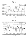
- Figs. 6C and 6D show the inner product of the first and second reference PC vectors with the first and second running PC vectors, respectively, as a function of time.
- the inner product is different from one.
- the inner product is 1.0 for PC1 and -1.0 for PC2, where the sign represents an increase or decrease of the signals, thereby indicating a match.
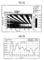
- Figs. 7A-D shows that for each of the times for which reference principal components were generated, the method was able to detect the same time during the production process in spite of the inclusion of random noise in the signal measured from the production process proving the robustness of the method of the present invention.
- Figs. 7B and 7C show that the PCA pattern recognition technique was successful in identifying the correct thickness of the film remaining after the etch process had proceeded for 20 seconds.
- the present invention was primarily described in conjunction with a plasma etch process, the invention can be used to monitor and control a variety of other plasma processes including both standard and high density plasma enhanced chemical vapor deposition processes among others.
- the invention can also be used to control non-plasma etch and deposition process (or processes where the plasma is formed remotely) by measuring wavelengths of radiation generated from a broadband lamp or similar light source reflected off the surface of the substrate being processed.
Landscapes
- Drying Of Semiconductors (AREA)
- Chemical Vapour Deposition (AREA)
Applications Claiming Priority (2)
| Application Number | Priority Date | Filing Date | Title |
|---|---|---|---|
| US09/470,828 US6413867B1 (en) | 1999-12-23 | 1999-12-23 | Film thickness control using spectral interferometry |
| US470828 | 1999-12-23 |
Publications (3)
| Publication Number | Publication Date |
|---|---|
| EP1111356A2 true EP1111356A2 (de) | 2001-06-27 |
| EP1111356A3 EP1111356A3 (de) | 2004-06-09 |
| EP1111356B1 EP1111356B1 (de) | 2008-11-05 |
Family
ID=23869222
Family Applications (1)
| Application Number | Title | Priority Date | Filing Date |
|---|---|---|---|
| EP00126312A Expired - Lifetime EP1111356B1 (de) | 1999-12-23 | 2000-12-01 | Verfahren und Vorrichtung zur Behandlung von Halbleitersubstraten |
Country Status (6)
| Country | Link |
|---|---|
| US (2) | US6413867B1 (de) |
| EP (1) | EP1111356B1 (de) |
| JP (1) | JP4925507B2 (de) |
| KR (1) | KR100748288B1 (de) |
| DE (1) | DE60040719D1 (de) |
| TW (1) | TW516075B (de) |
Cited By (16)
| Publication number | Priority date | Publication date | Assignee | Title |
|---|---|---|---|---|
| WO2003027609A1 (en) * | 2001-09-24 | 2003-04-03 | Applied Materials, Inc. | In-situ film thickness measurement using spectral interference at grazing incidence |
| WO2003102502A1 (de) * | 2002-05-29 | 2003-12-11 | Infineon Technologies Ag | Verfahren und vorrichtung zum ermitteln einer schichtdicke einer auf einem träger aufgebrachten schicht, sowie überwachungssystem |
| WO2004013907A1 (en) * | 2002-08-05 | 2004-02-12 | Advanced Micro Devices, Inc. | Dual damascene trench depth monitoring |
| WO2004015727A3 (en) * | 2002-08-13 | 2004-04-29 | Lam Res Corp | Method for controlling a recess etch process |
| WO2004059708A3 (en) * | 2002-12-20 | 2004-09-30 | Agere Systems Inc | Structure and method for bonding to copper interconnect structures |
| US6979578B2 (en) | 2002-08-13 | 2005-12-27 | Lam Research Corporation | Process endpoint detection method using broadband reflectometry |
| US7019844B2 (en) | 2002-08-13 | 2006-03-28 | Lam Research Corporation | Method for in-situ monitoring of patterned substrate processing using reflectometry. |
| DE102006035596A1 (de) * | 2006-07-27 | 2008-01-31 | Qimonda Ag | Verfahren und Anordnung zur Durchführung eines Ätz- oder Reinigungsschrittes |
| US7399711B2 (en) | 2002-08-13 | 2008-07-15 | Lam Research Corporation | Method for controlling a recess etch process |
| WO2008106207A3 (en) * | 2007-02-28 | 2008-12-31 | Advanced Micro Devices Inc | Technique for patterning differently stressed layers formed above transistors by enhanced etch control strategies |
| EP1376112B1 (de) * | 2002-06-27 | 2009-01-21 | Fraunhofer-Gesellschaft zur Förderung der angewandten Forschung e.V. | Verfahren zum Steuern eines Reinigungsvorgangs von Belägen auf einem Arbeitsteil |
| EP1647049A4 (de) * | 2003-07-22 | 2010-09-01 | Lam Res Corp | Verfahren und system zur elektronischen räumlichen filterung von optischen signalen eines spektralreflektometers |
| US7812966B2 (en) | 2007-08-30 | 2010-10-12 | Infineon Technologies Ag | Method of determining the depth profile of a surface structure and system for determining the depth profile of a surface structure |
| CN109631764A (zh) * | 2018-11-22 | 2019-04-16 | 南京理工大学 | 基于RealSense相机的尺寸测量系统及方法 |
| CN111834289A (zh) * | 2019-04-16 | 2020-10-27 | 中电海康集团有限公司 | 一种金属铝的刻蚀方法 |
| CN112461366A (zh) * | 2020-12-16 | 2021-03-09 | 四川长虹电器股份有限公司 | 一种基于随机滤波器阵列的近红外光谱仪实现方法 |
Families Citing this family (73)
| Publication number | Priority date | Publication date | Assignee | Title |
|---|---|---|---|---|
| US7037403B1 (en) * | 1992-12-28 | 2006-05-02 | Applied Materials Inc. | In-situ real-time monitoring technique and apparatus for detection of thin films during chemical/mechanical polishing planarization |
| US6614529B1 (en) * | 1992-12-28 | 2003-09-02 | Applied Materials, Inc. | In-situ real-time monitoring technique and apparatus for endpoint detection of thin films during chemical/mechanical polishing planarization |
| US7042580B1 (en) * | 1999-02-01 | 2006-05-09 | Tokyo Electron Limited | Apparatus for imaging metrology |
| US7177019B2 (en) * | 1999-02-01 | 2007-02-13 | Tokyo Electron Limited | Apparatus for imaging metrology |
| SE514718C2 (sv) * | 1999-06-29 | 2001-04-09 | Jan Otto Solem | Anordning för behandling av bristande tillslutningsförmåga hos mitralisklaffapparaten |
| US6368975B1 (en) * | 1999-07-07 | 2002-04-09 | Applied Materials, Inc. | Method and apparatus for monitoring a process by employing principal component analysis |
| TW499702B (en) * | 2000-07-04 | 2002-08-21 | Tokyo Electron Ltd | Method for monitoring operation of processing apparatus |
| US6936842B2 (en) * | 2001-06-27 | 2005-08-30 | Applied Materials, Inc. | Method and apparatus for process monitoring |
| JP3686866B2 (ja) * | 2001-12-18 | 2005-08-24 | 株式会社日立製作所 | 半導体製造装置及び製造方法 |
| US6960416B2 (en) * | 2002-03-01 | 2005-11-01 | Applied Materials, Inc. | Method and apparatus for controlling etch processes during fabrication of semiconductor devices |
| US7225047B2 (en) * | 2002-03-19 | 2007-05-29 | Applied Materials, Inc. | Method, system and medium for controlling semiconductor wafer processes using critical dimension measurements |
| US6943053B2 (en) * | 2002-03-20 | 2005-09-13 | Applied Materials, Inc. | System, method and medium for modeling, monitoring and/or controlling plasma based semiconductor manufacturing processes |
| US20030209518A1 (en) * | 2002-05-08 | 2003-11-13 | Taiwan Semiconductor Manufacturing Co., Ltd. | Method of detecting abnormal chamber conditions in etcher |
| US20040040658A1 (en) * | 2002-08-29 | 2004-03-04 | Tatehito Usui | Semiconductor fabricating apparatus and method and apparatus for determining state of semiconductor fabricating process |
| US6842661B2 (en) * | 2002-09-30 | 2005-01-11 | Advanced Micro Devices, Inc. | Process control at an interconnect level |
| US7265382B2 (en) * | 2002-11-12 | 2007-09-04 | Applied Materials, Inc. | Method and apparatus employing integrated metrology for improved dielectric etch efficiency |
| US7172792B2 (en) * | 2002-12-20 | 2007-02-06 | Applied Materials, Inc. | Method for forming a high quality low temperature silicon nitride film |
| US6904384B2 (en) * | 2003-04-03 | 2005-06-07 | Powerchip Semiconductor Corp. | Complex multivariate analysis system and method |
| US7482178B2 (en) * | 2003-08-06 | 2009-01-27 | Applied Materials, Inc. | Chamber stability monitoring using an integrated metrology tool |
| US6911399B2 (en) * | 2003-09-19 | 2005-06-28 | Applied Materials, Inc. | Method of controlling critical dimension microloading of photoresist trimming process by selective sidewall polymer deposition |
| US20050220984A1 (en) * | 2004-04-02 | 2005-10-06 | Applied Materials Inc., A Delaware Corporation | Method and system for control of processing conditions in plasma processing systems |
| DE102004018454A1 (de) * | 2004-04-16 | 2005-11-03 | Infineon Technologies Ag | Verfahren und Vorrichtung zum Überwachen des Ätzvorgangs einer regelmässigen Tiefenstruktur in einem Halbleitersubstrat |
| US20060000799A1 (en) * | 2004-06-30 | 2006-01-05 | Hyun-Ho Doh | Methods and apparatus for determining endpoint in a plasma processing system |
| US7363195B2 (en) * | 2004-07-07 | 2008-04-22 | Sensarray Corporation | Methods of configuring a sensor network |
| US20060012796A1 (en) * | 2004-07-14 | 2006-01-19 | Susumu Saito | Plasma treatment apparatus and light detection method of a plasma treatment |
| US7393459B2 (en) * | 2004-08-06 | 2008-07-01 | Applied Materials, Inc. | Method for automatic determination of substrates states in plasma processing chambers |
| US7250373B2 (en) * | 2004-08-27 | 2007-07-31 | Applied Materials, Inc. | Method and apparatus for etching material layers with high uniformity of a lateral etch rate across a substrate |
| US7601272B2 (en) * | 2005-01-08 | 2009-10-13 | Applied Materials, Inc. | Method and apparatus for integrating metrology with etch processing |
| US20060154388A1 (en) * | 2005-01-08 | 2006-07-13 | Richard Lewington | Integrated metrology chamber for transparent substrates |
| US7851368B2 (en) * | 2005-06-28 | 2010-12-14 | Lam Research Corporation | Methods and apparatus for igniting a low pressure plasma |
| US7566900B2 (en) * | 2005-08-31 | 2009-07-28 | Applied Materials, Inc. | Integrated metrology tools for monitoring and controlling large area substrate processing chambers |
| US7962113B2 (en) * | 2005-10-31 | 2011-06-14 | Silicon Laboratories Inc. | Receiver with multi-tone wideband I/Q mismatch calibration and method therefor |
| JP4833687B2 (ja) * | 2006-02-27 | 2011-12-07 | 株式会社日立ハイテクノロジーズ | プラズマ処理装置 |
| US7662646B2 (en) * | 2006-03-17 | 2010-02-16 | Tokyo Electron Limited | Plasma processing method and plasma processing apparatus for performing accurate end point detection |
| US20070249071A1 (en) * | 2006-04-21 | 2007-10-25 | Lei Lian | Neural Network Methods and Apparatuses for Monitoring Substrate Processing |
| KR100769566B1 (ko) * | 2006-05-24 | 2007-10-23 | 중앙대학교 산학협력단 | 신경망을 이용한 박막 두께 측정 방법, 장치 및 이를 위한기록매체 |
| US7469164B2 (en) * | 2006-06-26 | 2008-12-23 | Nanometrics Incorporated | Method and apparatus for process control with in-die metrology |
| US20080029484A1 (en) * | 2006-07-25 | 2008-02-07 | Applied Materials, Inc. | In-situ process diagnostics of in-film aluminum during plasma deposition |
| US20080063810A1 (en) * | 2006-08-23 | 2008-03-13 | Applied Materials, Inc. | In-situ process state monitoring of chamber |
| US7774082B2 (en) * | 2006-10-05 | 2010-08-10 | Tokyo Electron Limited | Substrate processing method and storage medium having program stored therein |
| US8017029B2 (en) | 2006-10-30 | 2011-09-13 | Applied Materials, Inc. | Plasma mask etch method of controlling a reactor tunable element in accordance with the output of an array of optical sensors viewing the mask backside |
| US8012366B2 (en) * | 2006-10-30 | 2011-09-06 | Applied Materials, Inc. | Process for etching a transparent workpiece including backside endpoint detection steps |
| US7976671B2 (en) * | 2006-10-30 | 2011-07-12 | Applied Materials, Inc. | Mask etch plasma reactor with variable process gas distribution |
| US20080099437A1 (en) * | 2006-10-30 | 2008-05-01 | Richard Lewington | Plasma reactor for processing a transparent workpiece with backside process endpoint detection |
| US9218944B2 (en) | 2006-10-30 | 2015-12-22 | Applied Materials, Inc. | Mask etch plasma reactor having an array of optical sensors viewing the workpiece backside and a tunable element controlled in response to the optical sensors |
| US7967930B2 (en) * | 2006-10-30 | 2011-06-28 | Applied Materials, Inc. | Plasma reactor for processing a workpiece and having a tunable cathode |
| US8002946B2 (en) * | 2006-10-30 | 2011-08-23 | Applied Materials, Inc. | Mask etch plasma reactor with cathode providing a uniform distribution of etch rate |
| US8520194B2 (en) | 2006-11-29 | 2013-08-27 | Macronix International Co., Ltd. | Method of forming a deposited material by utilizing a multi-step deposition/etch/deposition (D/E/D) process |
| US8184288B2 (en) | 2006-11-29 | 2012-05-22 | Macronix International Co., Ltd. | Method of depositing a silicon-containing material by utilizing a multi-step fill-in process in a deposition machine |
| US7813895B2 (en) * | 2007-07-27 | 2010-10-12 | Applied Materials, Inc. | Methods for plasma matching between different chambers and plasma stability monitoring and control |
| US20090065478A1 (en) * | 2007-09-11 | 2009-03-12 | Dockery Kevin P | Measuring etching rates using low coherence interferometry |
| GB0811991D0 (en) * | 2008-07-01 | 2008-08-06 | Scalar Technologies Ltd | Authentication apparatus and methods |
| US8101906B2 (en) | 2008-10-08 | 2012-01-24 | Applied Materials, Inc. | Method and apparatus for calibrating optical path degradation useful for decoupled plasma nitridation chambers |
| CN101834128B (zh) * | 2009-03-12 | 2012-03-21 | 中芯国际集成电路制造(上海)有限公司 | 半导体器件的制作方法 |
| JP5383265B2 (ja) | 2009-03-17 | 2014-01-08 | 株式会社日立ハイテクノロジーズ | エッチング装置、分析装置、エッチング処理方法、およびエッチング処理プログラム |
| JP5862433B2 (ja) | 2012-04-09 | 2016-02-16 | 株式会社島津製作所 | 表面処理状況モニタリング装置 |
| JP5888111B2 (ja) | 2012-05-18 | 2016-03-16 | 株式会社島津製作所 | エッチングモニタ装置 |
| JP2014002068A (ja) | 2012-06-19 | 2014-01-09 | Shimadzu Corp | 厚みモニタリング装置、エッチング深さモニタリング装置および厚みモニタリング方法 |
| US9818657B2 (en) * | 2013-06-21 | 2017-11-14 | Renesas Electronics Corporation | Dry etching method and method of manufacturing semiconductor device |
| JP6132688B2 (ja) * | 2013-07-18 | 2017-05-24 | 株式会社日立ハイテクノロジーズ | プラズマ処理装置及びプラズマ処理方法 |
| US10192763B2 (en) * | 2015-10-05 | 2019-01-29 | Applied Materials, Inc. | Methodology for chamber performance matching for semiconductor equipment |
| US10861755B2 (en) * | 2017-02-08 | 2020-12-08 | Verity Instruments, Inc. | System and method for measurement of complex structures |
| US10910201B1 (en) * | 2019-08-22 | 2021-02-02 | Tokyo Electron Limited | Synthetic wavelengths for endpoint detection in plasma etching |
| CN111081584B (zh) * | 2019-12-30 | 2022-07-19 | 中国科学院电子学研究所 | 基于光谱仪的离子刻蚀终点检测装置及应用其的刻蚀系统 |
| WO2022059114A1 (ja) * | 2020-09-17 | 2022-03-24 | 株式会社日立ハイテク | プラズマ処理装置およびプラズマ処理方法 |
| JP7587180B2 (ja) * | 2021-02-26 | 2024-11-20 | 日本電信電話株式会社 | 光導波路デバイスの製造方法および製造システム |
| JP7545093B2 (ja) * | 2021-02-26 | 2024-09-04 | 日本電信電話株式会社 | 光集積回路の製造システムおよび製造方法 |
| JP7545094B2 (ja) * | 2021-02-26 | 2024-09-04 | 日本電信電話株式会社 | 光集積回路の製造システムおよび製造方法 |
| WO2022180839A1 (ja) * | 2021-02-26 | 2022-09-01 | 日本電信電話株式会社 | 光導波路デバイスの製造方法および製造システム |
| US12218015B2 (en) * | 2021-04-16 | 2025-02-04 | Taiwan Semiconductor Manufacturing Company, Ltd. | Interferometer systems and methods for real time etch process compensation control |
| WO2024054380A1 (en) * | 2022-09-08 | 2024-03-14 | Lam Research Corporation | Multi-sensor determination of a state of semiconductor equipment |
| DE102024102041A1 (de) | 2024-01-24 | 2025-07-24 | Aixtron Se | Verfahren und Vorrichtung zur Ermittlung der Prozessfähigkeit eines Substrates |
| JPWO2026047926A1 (de) | 2024-08-29 | 2026-03-05 |
Family Cites Families (20)
| Publication number | Priority date | Publication date | Assignee | Title |
|---|---|---|---|---|
| US4602981A (en) * | 1985-05-06 | 1986-07-29 | International Business Machines Corporation | Monitoring technique for plasma etching |
| JPH0427120A (ja) * | 1990-05-23 | 1992-01-30 | Hitachi Ltd | 終点検出方法および装置 |
| JPH05197811A (ja) * | 1992-01-22 | 1993-08-06 | Mitsubishi Heavy Ind Ltd | パターン認識装置 |
| US5653894A (en) * | 1992-12-14 | 1997-08-05 | Lucent Technologies Inc. | Active neural network determination of endpoint in a plasma etch process |
| US5450205A (en) | 1993-05-28 | 1995-09-12 | Massachusetts Institute Of Technology | Apparatus and method for real-time measurement of thin film layer thickness and changes thereof |
| US5737496A (en) * | 1993-11-17 | 1998-04-07 | Lucent Technologies Inc. | Active neural network control of wafer attributes in a plasma etch process |
| EP0735565B1 (de) * | 1995-03-31 | 1999-06-02 | International Business Machines Corporation | Verfahren und Gerät zur Überwachung des Trockenätzens eines dielektrischen Films bis zu einer gegebenen Dicke |
| US5738756A (en) | 1995-06-30 | 1998-04-14 | Lam Research Corporation | Method and apparatus for detecting optimal endpoints in plasma etch processes |
| EP0756318A1 (de) | 1995-07-24 | 1997-01-29 | International Business Machines Corporation | Methode zur augenblicklichen in-situ-Überwachung eines Grabenformungsprozesses |
| US5658423A (en) * | 1995-11-27 | 1997-08-19 | International Business Machines Corporation | Monitoring and controlling plasma processes via optical emission using principal component analysis |
| US5846373A (en) * | 1996-06-28 | 1998-12-08 | Lam Research Corporation | Method for monitoring process endpoints in a plasma chamber and a process monitoring arrangement in a plasma chamber |
| US6018334A (en) | 1997-02-20 | 2000-01-25 | Eckerberg; Mark | Computer pointing device |
| US5926690A (en) | 1997-05-28 | 1999-07-20 | Advanced Micro Devices, Inc. | Run-to-run control process for controlling critical dimensions |
| US6153115A (en) * | 1997-10-23 | 2000-11-28 | Massachusetts Institute Of Technology | Monitor of plasma processes with multivariate statistical analysis of plasma emission spectra |
| US6148239A (en) | 1997-12-12 | 2000-11-14 | Advanced Micro Devices, Inc. | Process control system using feed forward control threads based on material groups |
| US6081334A (en) * | 1998-04-17 | 2000-06-27 | Applied Materials, Inc | Endpoint detection for semiconductor processes |
| US6136712A (en) * | 1998-09-30 | 2000-10-24 | Lam Research Corporation | Method and apparatus for improving accuracy of plasma etching process |
| US6052176A (en) | 1999-03-31 | 2000-04-18 | Lam Research Corporation | Processing chamber with optical window cleaned using process gas |
| US6160621A (en) * | 1999-09-30 | 2000-12-12 | Lam Research Corporation | Method and apparatus for in-situ monitoring of plasma etch and deposition processes using a pulsed broadband light source |
| US6245581B1 (en) | 2000-04-19 | 2001-06-12 | Advanced Micro Devices, Inc. | Method and apparatus for control of critical dimension using feedback etch control |
-
1999
- 1999-12-23 US US09/470,828 patent/US6413867B1/en not_active Expired - Lifetime
-
2000
- 2000-11-08 TW TW089123642A patent/TW516075B/zh not_active IP Right Cessation
- 2000-12-01 DE DE60040719T patent/DE60040719D1/de not_active Expired - Lifetime
- 2000-12-01 EP EP00126312A patent/EP1111356B1/de not_active Expired - Lifetime
- 2000-12-22 KR KR1020000080204A patent/KR100748288B1/ko not_active Expired - Fee Related
- 2000-12-25 JP JP2000392867A patent/JP4925507B2/ja not_active Expired - Fee Related
-
2002
- 2002-04-23 US US10/131,726 patent/US6589869B2/en not_active Expired - Fee Related
Cited By (26)
| Publication number | Priority date | Publication date | Assignee | Title |
|---|---|---|---|---|
| WO2003027609A1 (en) * | 2001-09-24 | 2003-04-03 | Applied Materials, Inc. | In-situ film thickness measurement using spectral interference at grazing incidence |
| WO2003102502A1 (de) * | 2002-05-29 | 2003-12-11 | Infineon Technologies Ag | Verfahren und vorrichtung zum ermitteln einer schichtdicke einer auf einem träger aufgebrachten schicht, sowie überwachungssystem |
| EP1376112B1 (de) * | 2002-06-27 | 2009-01-21 | Fraunhofer-Gesellschaft zur Förderung der angewandten Forschung e.V. | Verfahren zum Steuern eines Reinigungsvorgangs von Belägen auf einem Arbeitsteil |
| WO2004013907A1 (en) * | 2002-08-05 | 2004-02-12 | Advanced Micro Devices, Inc. | Dual damascene trench depth monitoring |
| US7399711B2 (en) | 2002-08-13 | 2008-07-15 | Lam Research Corporation | Method for controlling a recess etch process |
| WO2004015727A3 (en) * | 2002-08-13 | 2004-04-29 | Lam Res Corp | Method for controlling a recess etch process |
| US6979578B2 (en) | 2002-08-13 | 2005-12-27 | Lam Research Corporation | Process endpoint detection method using broadband reflectometry |
| US7019844B2 (en) | 2002-08-13 | 2006-03-28 | Lam Research Corporation | Method for in-situ monitoring of patterned substrate processing using reflectometry. |
| US7531369B2 (en) | 2002-08-13 | 2009-05-12 | Lam Research Corporation | Process endpoint detection method using broadband reflectometry |
| US7328830B2 (en) | 2002-12-20 | 2008-02-12 | Agere Systems Inc. | Structure and method for bonding to copper interconnect structures |
| WO2004059708A3 (en) * | 2002-12-20 | 2004-09-30 | Agere Systems Inc | Structure and method for bonding to copper interconnect structures |
| GB2411767A (en) * | 2002-12-20 | 2005-09-07 | Agere Systems Inc | Structure and method for bonding to copper interconnect structures |
| GB2411767B (en) * | 2002-12-20 | 2006-11-01 | Agere Systems Inc | Structure and method for bonding to copper interconnect structures |
| EP1647049A4 (de) * | 2003-07-22 | 2010-09-01 | Lam Res Corp | Verfahren und system zur elektronischen räumlichen filterung von optischen signalen eines spektralreflektometers |
| DE102006035596B4 (de) * | 2006-07-27 | 2008-04-30 | Qimonda Ag | Verfahren und Anordnung zur Durchführung eines Ätz- oder Reinigungsschrittes |
| DE102006035596A1 (de) * | 2006-07-27 | 2008-01-31 | Qimonda Ag | Verfahren und Anordnung zur Durchführung eines Ätz- oder Reinigungsschrittes |
| US7883629B2 (en) | 2007-02-28 | 2011-02-08 | Globalfoundries Inc. | Technique for patterning differently stressed layers formed above transistors by enhanced etch control strategies |
| WO2008106207A3 (en) * | 2007-02-28 | 2008-12-31 | Advanced Micro Devices Inc | Technique for patterning differently stressed layers formed above transistors by enhanced etch control strategies |
| US7812966B2 (en) | 2007-08-30 | 2010-10-12 | Infineon Technologies Ag | Method of determining the depth profile of a surface structure and system for determining the depth profile of a surface structure |
| DE102008039322B4 (de) * | 2007-08-30 | 2014-06-12 | Infineon Technologies Ag | Verfahren zum Ermitteln des Tiefenprofils einer Oberflächenstruktur und System zum Ermitteln des Tiefenprofils einer Oberflächenstruktur |
| CN109631764A (zh) * | 2018-11-22 | 2019-04-16 | 南京理工大学 | 基于RealSense相机的尺寸测量系统及方法 |
| CN109631764B (zh) * | 2018-11-22 | 2020-12-04 | 南京理工大学 | 基于RealSense相机的尺寸测量系统及方法 |
| CN111834289A (zh) * | 2019-04-16 | 2020-10-27 | 中电海康集团有限公司 | 一种金属铝的刻蚀方法 |
| CN111834289B (zh) * | 2019-04-16 | 2022-10-28 | 中电海康集团有限公司 | 一种金属铝的刻蚀方法 |
| CN112461366A (zh) * | 2020-12-16 | 2021-03-09 | 四川长虹电器股份有限公司 | 一种基于随机滤波器阵列的近红外光谱仪实现方法 |
| CN112461366B (zh) * | 2020-12-16 | 2021-12-21 | 四川长虹电器股份有限公司 | 一种基于随机滤波器阵列的近红外光谱仪实现方法 |
Also Published As
| Publication number | Publication date |
|---|---|
| US6589869B2 (en) | 2003-07-08 |
| KR100748288B1 (ko) | 2007-08-09 |
| DE60040719D1 (de) | 2008-12-18 |
| JP4925507B2 (ja) | 2012-04-25 |
| EP1111356B1 (de) | 2008-11-05 |
| TW516075B (en) | 2003-01-01 |
| US6413867B1 (en) | 2002-07-02 |
| KR20010070338A (ko) | 2001-07-25 |
| US20020119660A1 (en) | 2002-08-29 |
| EP1111356A3 (de) | 2004-06-09 |
| JP2001244254A (ja) | 2001-09-07 |
Similar Documents
| Publication | Publication Date | Title |
|---|---|---|
| US6413867B1 (en) | Film thickness control using spectral interferometry | |
| JP4833396B2 (ja) | 主成分分析を用いてプロセスをモニタするための方法 | |
| US20230097892A1 (en) | Optical diagnostics of semiconductor process using hyperspectral imaging | |
| EP1218689B1 (de) | Verfahren und vorrichtung für die in-situ-messung von plasma-ätz-prozessen und plasma-abscheidungs-prozessen mit hilfe einer breitbandigen gepulsten lichtquelle | |
| US6673200B1 (en) | Method of reducing process plasma damage using optical spectroscopy | |
| US6815228B2 (en) | Film thickness measuring method of member to be processed using emission spectroscopy and processing method of the member using the measuring method | |
| US8747608B2 (en) | Plasma processing apparatus | |
| JP3854810B2 (ja) | 発光分光法による被処理材の膜厚測定方法及び装置とそれを用いた被処理材の処理方法及び装置 | |
| US6824813B1 (en) | Substrate monitoring method and apparatus | |
| KR20030000274A (ko) | 반도체 제조공정에서 실시간 플라즈마 측정과 박막분석을위한 다채널 분광분석기 | |
| JP2001093885A (ja) | エッチング監視装置 | |
| US8085390B2 (en) | Multivariate monitoring method for plasma process machine | |
| KR20010099591A (ko) | 프로세스 모니터 | |
| US7599058B2 (en) | Methods for plasma diagnostics and the measurement of thin films | |
| US6605482B2 (en) | Process for monitoring the thickness of layers in a microelectronic device | |
| JP2006119145A (ja) | 半導体ウエハの処理方法及び処理装置 | |
| KR100733120B1 (ko) | 반도체 웨이퍼처리의 검출방법 및 검출장치 | |
| JP2013507635A (ja) | 原位置における極薄の光学膜の厚さデータ決定のための方法およびシステム | |
| TW200401885A (en) | Method and device for determining the thickness of a layer applied to a carrier, and monitoring system | |
| JP2000306821A (ja) | ベーク終了検知装置 |
Legal Events
| Date | Code | Title | Description |
|---|---|---|---|
| PUAI | Public reference made under article 153(3) epc to a published international application that has entered the european phase |
Free format text: ORIGINAL CODE: 0009012 |
|
| AK | Designated contracting states |
Kind code of ref document: A2 Designated state(s): AT BE CH CY DE DK ES FI FR GB GR IE IT LI LU MC NL PT SE TR |
|
| AX | Request for extension of the european patent |
Free format text: AL;LT;LV;MK;RO;SI |
|
| PUAL | Search report despatched |
Free format text: ORIGINAL CODE: 0009013 |
|
| AK | Designated contracting states |
Kind code of ref document: A3 Designated state(s): AT BE CH CY DE DK ES FI FR GB GR IE IT LI LU MC NL PT SE TR |
|
| AX | Request for extension of the european patent |
Extension state: AL LT LV MK RO SI |
|
| RIC1 | Information provided on ipc code assigned before grant |
Ipc: 7H 01J 37/32 B Ipc: 7G 01B 11/06 B Ipc: 7G 01J 3/28 A Ipc: 7H 01L 21/66 B |
|
| AKX | Designation fees paid | ||
| REG | Reference to a national code |
Ref country code: DE Ref legal event code: 8566 |
|
| 17P | Request for examination filed |
Effective date: 20050218 |
|
| RBV | Designated contracting states (corrected) |
Designated state(s): BE CH DE FR GB LI NL |
|
| 17Q | First examination report despatched |
Effective date: 20050406 |
|
| GRAP | Despatch of communication of intention to grant a patent |
Free format text: ORIGINAL CODE: EPIDOSNIGR1 |
|
| GRAS | Grant fee paid |
Free format text: ORIGINAL CODE: EPIDOSNIGR3 |
|
| GRAA | (expected) grant |
Free format text: ORIGINAL CODE: 0009210 |
|
| AK | Designated contracting states |
Kind code of ref document: B1 Designated state(s): BE CH DE FR GB LI NL |
|
| REG | Reference to a national code |
Ref country code: GB Ref legal event code: FG4D |
|
| REG | Reference to a national code |
Ref country code: CH Ref legal event code: EP |
|
| REF | Corresponds to: |
Ref document number: 60040719 Country of ref document: DE Date of ref document: 20081218 Kind code of ref document: P |
|
| NLV1 | Nl: lapsed or annulled due to failure to fulfill the requirements of art. 29p and 29m of the patents act | ||
| PG25 | Lapsed in a contracting state [announced via postgrant information from national office to epo] |
Ref country code: NL Free format text: LAPSE BECAUSE OF FAILURE TO SUBMIT A TRANSLATION OF THE DESCRIPTION OR TO PAY THE FEE WITHIN THE PRESCRIBED TIME-LIMIT Effective date: 20081105 |
|
| PG25 | Lapsed in a contracting state [announced via postgrant information from national office to epo] |
Ref country code: BE Free format text: LAPSE BECAUSE OF FAILURE TO SUBMIT A TRANSLATION OF THE DESCRIPTION OR TO PAY THE FEE WITHIN THE PRESCRIBED TIME-LIMIT Effective date: 20081105 |
|
| REG | Reference to a national code |
Ref country code: CH Ref legal event code: PL |
|
| PLBE | No opposition filed within time limit |
Free format text: ORIGINAL CODE: 0009261 |
|
| STAA | Information on the status of an ep patent application or granted ep patent |
Free format text: STATUS: NO OPPOSITION FILED WITHIN TIME LIMIT |
|
| 26N | No opposition filed |
Effective date: 20090806 |
|
| GBPC | Gb: european patent ceased through non-payment of renewal fee |
Effective date: 20090205 |
|
| PG25 | Lapsed in a contracting state [announced via postgrant information from national office to epo] |
Ref country code: CH Free format text: LAPSE BECAUSE OF NON-PAYMENT OF DUE FEES Effective date: 20081231 Ref country code: LI Free format text: LAPSE BECAUSE OF NON-PAYMENT OF DUE FEES Effective date: 20081231 |
|
| PGFP | Annual fee paid to national office [announced via postgrant information from national office to epo] |
Ref country code: FR Payment date: 20090206 Year of fee payment: 9 |
|
| PG25 | Lapsed in a contracting state [announced via postgrant information from national office to epo] |
Ref country code: GB Free format text: LAPSE BECAUSE OF NON-PAYMENT OF DUE FEES Effective date: 20090205 |
|
| REG | Reference to a national code |
Ref country code: FR Ref legal event code: ST Effective date: 20100831 |
|
| PG25 | Lapsed in a contracting state [announced via postgrant information from national office to epo] |
Ref country code: FR Free format text: LAPSE BECAUSE OF NON-PAYMENT OF DUE FEES Effective date: 20091231 |
|
| PGFP | Annual fee paid to national office [announced via postgrant information from national office to epo] |
Ref country code: DE Payment date: 20131230 Year of fee payment: 14 |
|
| REG | Reference to a national code |
Ref country code: DE Ref legal event code: R119 Ref document number: 60040719 Country of ref document: DE |
|
| PG25 | Lapsed in a contracting state [announced via postgrant information from national office to epo] |
Ref country code: DE Free format text: LAPSE BECAUSE OF NON-PAYMENT OF DUE FEES Effective date: 20150701 |