EP1111472B1 - Appareil lithographique avec un système de détection de position - Google Patents
Appareil lithographique avec un système de détection de position Download PDFInfo
- Publication number
- EP1111472B1 EP1111472B1 EP20000311469 EP00311469A EP1111472B1 EP 1111472 B1 EP1111472 B1 EP 1111472B1 EP 20000311469 EP20000311469 EP 20000311469 EP 00311469 A EP00311469 A EP 00311469A EP 1111472 B1 EP1111472 B1 EP 1111472B1
- Authority
- EP
- European Patent Office
- Prior art keywords
- radiation
- detector
- substrate
- reference frame
- object table
- Prior art date
- Legal status (The legal status is an assumption and is not a legal conclusion. Google has not performed a legal analysis and makes no representation as to the accuracy of the status listed.)
- Expired - Lifetime
Links
- 238000001514 detection method Methods 0.000 title claims description 22
- 230000005855 radiation Effects 0.000 claims description 60
- 239000000758 substrate Substances 0.000 claims description 49
- 238000000034 method Methods 0.000 claims description 13
- 238000000059 patterning Methods 0.000 claims description 12
- 238000004519 manufacturing process Methods 0.000 claims description 7
- 238000005286 illumination Methods 0.000 claims description 6
- 238000003384 imaging method Methods 0.000 claims description 5
- 239000000463 material Substances 0.000 claims description 5
- 239000011248 coating agent Substances 0.000 claims description 3
- 238000000576 coating method Methods 0.000 claims description 3
- 239000013307 optical fiber Substances 0.000 claims description 3
- 239000010410 layer Substances 0.000 description 9
- 238000005259 measurement Methods 0.000 description 9
- 238000006073 displacement reaction Methods 0.000 description 6
- 230000008569 process Effects 0.000 description 5
- 230000008901 benefit Effects 0.000 description 3
- 230000035945 sensitivity Effects 0.000 description 3
- 230000003068 static effect Effects 0.000 description 3
- 241000282326 Felis catus Species 0.000 description 2
- XUIMIQQOPSSXEZ-UHFFFAOYSA-N Silicon Chemical compound [Si] XUIMIQQOPSSXEZ-UHFFFAOYSA-N 0.000 description 2
- 238000010894 electron beam technology Methods 0.000 description 2
- 230000006870 function Effects 0.000 description 2
- 150000002500 ions Chemical class 0.000 description 2
- 230000003287 optical effect Effects 0.000 description 2
- 239000002245 particle Substances 0.000 description 2
- 230000010363 phase shift Effects 0.000 description 2
- 238000005070 sampling Methods 0.000 description 2
- 238000007493 shaping process Methods 0.000 description 2
- 229910052710 silicon Inorganic materials 0.000 description 2
- 239000010703 silicon Substances 0.000 description 2
- 229910001374 Invar Inorganic materials 0.000 description 1
- 239000006094 Zerodur Substances 0.000 description 1
- 238000003491 array Methods 0.000 description 1
- 230000002238 attenuated effect Effects 0.000 description 1
- 230000005540 biological transmission Effects 0.000 description 1
- 230000008859 change Effects 0.000 description 1
- 238000012512 characterization method Methods 0.000 description 1
- 238000010276 construction Methods 0.000 description 1
- 230000008878 coupling Effects 0.000 description 1
- 238000010168 coupling process Methods 0.000 description 1
- 238000005859 coupling reaction Methods 0.000 description 1
- 230000001186 cumulative effect Effects 0.000 description 1
- 230000001419 dependent effect Effects 0.000 description 1
- 238000013461 design Methods 0.000 description 1
- 238000011161 development Methods 0.000 description 1
- 238000009826 distribution Methods 0.000 description 1
- 230000005670 electromagnetic radiation Effects 0.000 description 1
- 238000005530 etching Methods 0.000 description 1
- 230000004907 flux Effects 0.000 description 1
- 230000001939 inductive effect Effects 0.000 description 1
- 238000007689 inspection Methods 0.000 description 1
- 238000005468 ion implantation Methods 0.000 description 1
- 238000010884 ion-beam technique Methods 0.000 description 1
- 239000002346 layers by function Substances 0.000 description 1
- 239000007788 liquid Substances 0.000 description 1
- 239000004973 liquid crystal related substance Substances 0.000 description 1
- 238000001459 lithography Methods 0.000 description 1
- 230000005381 magnetic domain Effects 0.000 description 1
- 239000011159 matrix material Substances 0.000 description 1
- 230000015654 memory Effects 0.000 description 1
- QSHDDOUJBYECFT-UHFFFAOYSA-N mercury Chemical compound [Hg] QSHDDOUJBYECFT-UHFFFAOYSA-N 0.000 description 1
- 229910052753 mercury Inorganic materials 0.000 description 1
- 238000001465 metallisation Methods 0.000 description 1
- 230000003647 oxidation Effects 0.000 description 1
- 238000007254 oxidation reaction Methods 0.000 description 1
- 238000005498 polishing Methods 0.000 description 1
- 230000037452 priming Effects 0.000 description 1
- 238000012545 processing Methods 0.000 description 1
- 239000004065 semiconductor Substances 0.000 description 1
- 238000003860 storage Methods 0.000 description 1
- 239000010409 thin film Substances 0.000 description 1
- 238000012546 transfer Methods 0.000 description 1
Images

Classifications
-
- G—PHYSICS
- G03—PHOTOGRAPHY; CINEMATOGRAPHY; ANALOGOUS TECHNIQUES USING WAVES OTHER THAN OPTICAL WAVES; ELECTROGRAPHY; HOLOGRAPHY
- G03F—PHOTOMECHANICAL PRODUCTION OF TEXTURED OR PATTERNED SURFACES, e.g. FOR PRINTING, FOR PROCESSING OF SEMICONDUCTOR DEVICES; MATERIALS THEREFOR; ORIGINALS THEREFOR; APPARATUS SPECIALLY ADAPTED THEREFOR
- G03F9/00—Registration or positioning of originals, masks, frames, photographic sheets or textured or patterned surfaces, e.g. automatically
- G03F9/70—Registration or positioning of originals, masks, frames, photographic sheets or textured or patterned surfaces, e.g. automatically for microlithography
- G03F9/7003—Alignment type or strategy, e.g. leveling, global alignment
- G03F9/7007—Alignment other than original with workpiece
- G03F9/7015—Reference, i.e. alignment of original or workpiece with respect to a reference not on the original or workpiece
-
- G—PHYSICS
- G03—PHOTOGRAPHY; CINEMATOGRAPHY; ANALOGOUS TECHNIQUES USING WAVES OTHER THAN OPTICAL WAVES; ELECTROGRAPHY; HOLOGRAPHY
- G03F—PHOTOMECHANICAL PRODUCTION OF TEXTURED OR PATTERNED SURFACES, e.g. FOR PRINTING, FOR PROCESSING OF SEMICONDUCTOR DEVICES; MATERIALS THEREFOR; ORIGINALS THEREFOR; APPARATUS SPECIALLY ADAPTED THEREFOR
- G03F7/00—Photomechanical, e.g. photolithographic, production of textured or patterned surfaces, e.g. printing surfaces; Materials therefor, e.g. comprising photoresists; Apparatus specially adapted therefor
- G03F7/70—Microphotolithographic exposure; Apparatus therefor
- G03F7/70691—Handling of masks or workpieces
- G03F7/70716—Stages
-
- G—PHYSICS
- G03—PHOTOGRAPHY; CINEMATOGRAPHY; ANALOGOUS TECHNIQUES USING WAVES OTHER THAN OPTICAL WAVES; ELECTROGRAPHY; HOLOGRAPHY
- G03F—PHOTOMECHANICAL PRODUCTION OF TEXTURED OR PATTERNED SURFACES, e.g. FOR PRINTING, FOR PROCESSING OF SEMICONDUCTOR DEVICES; MATERIALS THEREFOR; ORIGINALS THEREFOR; APPARATUS SPECIALLY ADAPTED THEREFOR
- G03F9/00—Registration or positioning of originals, masks, frames, photographic sheets or textured or patterned surfaces, e.g. automatically
- G03F9/70—Registration or positioning of originals, masks, frames, photographic sheets or textured or patterned surfaces, e.g. automatically for microlithography
- G03F9/7049—Technique, e.g. interferometric
Definitions
- the present invention relates to the use of the position detection system in lithographic projection apparatus comprising:
- patterning means should be broadly interpreted as referring to means that can be used to endow an incoming radiation beam with a patterned cross-section, corresponding to a pattern that is to be created in a target portion of the substrate; the term “light valve” has also been used in this context.
- the said pattern will correspond to a particular functional layer in a device being created in the target portion, such as an integrated circuit or other device (see below). Examples of such patterning means include:
- the projection system may hereinafter be referred to as the "lens"; however, this term should be broadly interpreted as encompassing various types of projection system, including refractive optics, reflective optics, and catadioptric systems, for example.
- the illumination system may also include components operating according to any of these design types for directing, shaping or controlling the projection beam of radiation, and such components may also be referred to below, collectively or singularly, as a “lens”.
- the first and second object tables may be referred to as the "mask table” and the "substrate table", respectively.
- Lithographic projection apparatus can be used, for example, in the manufacture of integrated circuits (ICs).
- the patterning means may generate a circuit pattern corresponding to an individual layer of the IC, and this pattern can be imaged onto a target portion (comprising one or more dies) on a substrate (silicon wafer) that has been coated with a layer of radiation-sensitive material (resist).
- a target portion comprising one or more dies
- a substrate silicon wafer
- a layer of radiation-sensitive material resist
- a single wafer will contain a whole network of adjacent target portions that are successively irradiated via the projection system, one at a time.
- employing patterning by a mask on a mask table a distinction can be made between two different types of machine.
- each target portion is irradiated by exposing the entire mask pattern onto the target portion in one go; such an apparatus is commonly referred to as wafer stepper.
- a step-and-scan apparatus each target portion is irradiated by progressively scanning the mask pattern under the projection beam in a given reference direction (the "scanning" direction) while synchronously scanning the substrate table parallel or anti-parallel to this direction; since, in general, the projection system will have a magnification factor M (generally ⁇ 1), the speed V at which the substrate table is scanned will be a factor M times that at which the mask table is scanned.
- M magnification factor
- apparatus of this type contained a single first object (mask) table and a single second object (substrate) table.
- first object mask
- second object substrate
- machines are becoming available in which there are at least two independently movable substrate tables; see, for example, the multi-stage apparatus described in US 5,969,441 and US Serial No. 09/180,011, filed 27 February, 1998 (WO 98/40791).
- the basic operating principle behind such a multi-stage apparatus is that, while a first substrate table is underneath the projection system so as to allow exposure of a first substrate located on that table, a second substrate table can run to a loading position, discharge an exposed substrate, pick up a new substrate, perform some initial metrology steps on the new substrate, and then stand by to transfer this new substrate to the exposure position underneath the projection system as soon as exposure of the first substrate is completed, whence the cycle repeats itself; in this manner, it is possible to achieve a substantially increased machine throughout, which in turn improves the cost of ownership of the machine.
- lithographic projection apparatus In a lithographic apparatus, the size of features that can be imaged onto the substrate is limited by the wavelength of the projection radiation. To produce integrated circuits with a higher density of devices and hence higher operating speeds, it is desirable to be able to image smaller features. Whilst most current lithographic projection apparatus employ ultraviolet light generated by mercury lamps or excimer lasers, it has been proposed to use higher frequency (energy) radiation, e.g. EUV or X-rays, or particle beams, e.g. electrons or ions, as the projection radiation in lithographic apparatus.
- EUV ultraviolet light generated by mercury lamps or excimer lasers
- particle beams e.g. electrons or ions
- a substrate or mask positioning system it is often desirable to be able to position the mask or substrate in all 6 degrees of freedom (DOF).
- DOF degrees of freedom
- Six zero reference systems and six incremental positioning systems are therefore coupled together in a kinematic chain which can result in cumulative repeatability errors which are unacceptably high.
- the zero reference of the holder is often referenced to a vibration-isolated reference frame, onto which only the most critical metrology components are mounted.
- Zero references of encoder systems for coarse positioning do not fit into this category and so are mounted on separate structures, the position of which remains undefined at micrometer level relative to the isolated reference frame.
- US 4,676,649 discloses an interferometer system using plane mirrors mounted on moveable objects and fringe counters.
- GB 2,297,87 discloses a distance measurement device in which an astigmatic liquid beam is to be measured. The shape of the reflected beam on a detector is indicative of the distance of the object.
- An object of the present invention is to provide a referencing system which allows repeatable referencing, preferably to sub-micrometer accuracy, of a moveable object relative to a reference frame. Ideally the system should provide the ability to reference the moveable object in six degrees of freedom simultaneously.
- the above described position detection device can measure the position of the object table in two degrees of freedom; to detect its position in six degrees of freedom, three such position detection devices having mutually different (i.e. not parallel), preferably substantially orthogonal, orientations may be provided in the lithographic projection apparatus.
- the radiation source is preferably a source of collimated radiation and may comprise a monochromatic light source such as an LED or laser diode mounted on the sensor housing or away from the reference frame and with an optical fiber to bring light emitted by said light source to beam directing optics mounted on said reference frame.
- a monochromatic light source such as an LED or laser diode mounted on the sensor housing or away from the reference frame and with an optical fiber to bring light emitted by said light source to beam directing optics mounted on said reference frame.
- the two-dimensional position detector may be a two-dimensional PSD (position sensing detector), a CCD camera, a four quadrant photo-detector or any suitable two-dimensional detector array which can provide an output signal in each of two orthogonal directions as a function of the position of the reflected light beam on the detector (array).
- the resolution of a CCD camera used in the invention may be enhanced by sub-pixel interpolation.
- a pattern in a mask is imaged onto a substrate which is at least partially covered by a layer of radiation-sensitive material (resist).
- the substrate Prior to this imaging step, the substrate may undergo various procedures, such as priming, resist coating and a soft bake. After exposure, the substrate may be subjected to other procedures, such as a post-exposure bake (PEB), development, a hard bake and measurement/inspection of the imaged features.
- PEB post-exposure bake
- This array of procedures is used as a basis to pattern an individual layer of a device, e.g. an IC.
- Such a patterned layer may then undergo various processes such as etching, ion-implantation (doping), metallisation, oxidation, chemo-mechanical polishing, etc., all intended to finish off an individual layer. If several layers are required, then the whole procedure, or a variant thereof, will have to be repeated for each new layer. Eventually, an array of devices will be present on the substrate (wafer). These devices are then separated from one another by a technique such as dicing or sawing, whence the individual devices can be mounted on a carrier, connected to pins, etc. Further information regarding such processes can be obtained, for example, from the book “Microchip Fabrication: A Practical Guide to Semiconductor Processing", Third Edition, by Peter van Zant, McGraw Hill Publishing Co., 1997, ISBN 0-07-067250-4.
- UV radiation e.g. at a wavelength of 365nm, 248 nm, 193 nm, 157nm or 126nm
- EUV radiation extreme ultraviolet radiation
- X-rays electrons and ions.
- Figure 1 schematically depicts a lithographic projection apparatus according to the invention.
- the apparatus comprises:
- the radiation system comprises a source LA (e.g. a Hg lamp, excimer laser, a laser-produced or discharge plasma source, an undulator provided around the path of an electron beam in a storage ring or synchrotron, or an electron or ion beam source) which produces a beam of radiation.
- a source LA e.g. a Hg lamp, excimer laser, a laser-produced or discharge plasma source, an undulator provided around the path of an electron beam in a storage ring or synchrotron, or an electron or ion beam source
- This beam is passed along various optical components comprised in the illumination system II., - e.g. beam shaping optics Ex, an integrator IN and a condenser CO -so that the resultant beam PB has a desired shape and intensity distribution.
- the beam PB subsequently intercepts the mask MA which is held in a mask holder on a mask table MT. Having passed through the mask MA, the beam PB passes through the lens PL, which focuses the beam PB onto a target portion C of the substrate W.
- the substrate table WT can be moved accurately by the second positioning means, e.g. so as to position different target portions C in the path of the beam PB.
- the first positioning means and interferometric displacement measuring means can be used to accurately position the mask MA with respect to the path of the beam PB, e.g. after mechanical retrieval of the mask MA from a mask library.
- movement of the object tables MT, WT will be realized with the aid of a long stroke module (course positioning) and a short stroke module (fine positioning), which are not explicitly depicted in Figure 1.
- the depicted apparatus can be used in two different modes:
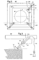
- FIG. 2 shows in plan an embodiment of the present invention used in conjunction with the substrate (wafer) table WT. It will be appreciated that the present invention can also be used with a mask (reticle) table.
- the wafer W and reference X & Y-axes are shown in phantom.
- the Z-axis is normal to the X and Y-axes.
- the position detection system according to the invention comprises three similar position detection apparatus 10A, 10B, 10C.
- Each position detection apparatus comprises a radiation source 11 which emits an incident beam 12 of collimated radiation towards a retro-reflector 13, that is a reflector which reflects the incident light onto a return path that is parallel to but displaced from the incident light path.
- the displacement of the return beam 14, in two dimensions, is a function of the relative position of the radiation source and the reflector in a plane normal to the incident beam 12.
- the retro-reflector 13 may, for example, be constructed from three mutually perpendicular plane reflectors meeting at a single corner, a so-called "corner cube".
- the reflectors may be formed by providing a mirror coating on three external faces of a corner (notionally) cut from a transmissive cube.
- the return beam 14 impinges on a two-dimensional radiation detector 15.
- the radiation source 11 and radiation detector 15 are mounted adjacent to one another and on the isolated reference or metrology frame MF of the lithographic apparatus in a highly stable manner.
- the radiation source 11 and radiation detector 15 may be mounted to each other or to a single bracket 16, shown in Figure 3.
- the housing(s) and/or mounting bracket(s) of the position detector 15 and radiation source 11 are preferably made of a material with very low thermal coefficient of expansion, such as Zerodur (RTM) or Invar, for high thermal stability.
- the isolated reference or metrology frame MF may also be made of such a material.
- the retro-reflector 13 is mounted on the wafer table WT at a convenient location, e.g. near one corner.
- the two-dimensional position detector 15 may be a two-dimensional PSD (position sensing detector), a CCD camera, a four quadrant photo-detector or any suitable two-dimensional detector array and is mounted with its sensing plane substantially perpendicular to the incident and reflected beams 12, 14.
- PSD position sensing detector
- CCD camera CCD camera
- four quadrant photo-detector any suitable two-dimensional detector array and is mounted with its sensing plane substantially perpendicular to the incident and reflected beams 12, 14.
- the positions of the position detection apparatus 10A, 10B, 10C and their orientations, i.e. angles ⁇ , ⁇ , ⁇ , are selected to provide the highest possible balanced positional sensitivity in all 6 degrees of freedom.
- the position and orientations of the position detection apparatus will be determined by factors such as the shape of the substrate table and reference frame as well as the differing sensitivities of the lithographic apparatus to positional, pitch, roll and yaw errors.
- Figure 3 is a partial cross-sectional view of one position detection apparatus 10.
- the radiation source 11 and radiation detector 15 are mounted via bracket 16 to the metrology frame MF at such a position that the incident and return beams 12, 14 are inclined at an angle ⁇ to the X-Y plane, to which the wafer W is substantially parallel.
- Angle ⁇ is preferably substantially 45E so that horizontal and vertical displacements of the reflector 13 relative to the incident light beam 12 of equal magnitude result in equal displacement of the return light beam 14 on the radiation detector 15.
- the radiation source 11 is formed of a LED or laser diode 111 or a similar monochromatic light source for emitting light into a single mode optical fiber 112 which leads that light to collimating optics 113 mounted on the metrology frame MF.
- the light source 111 can be placed away from the metrology frame MF and thermally isolated from it.
- the removal of the light source from the detector housing also leads to much higher pointing stability of the collimated beam with respect to the sensor/detector.
- Figure 4 shows a possible arrangement of a corner cube reflector 13 inset into the substrate table WT.
- the light source 11 directs the incident beam 12 into corner cube reflector 13 via aperture 17.
- the incident beam 12 is normal to the upper surface of the substrate table WT and is reflected by the three faces 13a, 13b, 13c of the corner cube reflector 13 so that the return beam 14 is on a parallel path to detector 15.
- the position detection apparatus detects displacement in directions parallel to the upper surface of the substrate table WT.
- retro-reflector 13N known as a cat's-eye
- the cat's-eye 13N comprises a lens 131 and a mirror 132 placed at a distance for the lens 131 equal to its focal length, f.
- the lens 131 is formed in the carved front surface of a single transparent body 133 which has a plane rear surface that is selectively silvered to form mirror 132.
- the three position detection devices of the invention forming a position sensing system, provide six signals dependent on the position and orientation of the wafer table WT.
- the system can be used in two modes:
- the positions of the radiation source/detector units on the metrology (reference) frame and the reflectors on the table are such that the table can be moved to a position where zero outputs are given for all six degrees of freedom simultaneously.
- the "zero" position need not be the position at which all detectors give their zero or mid range outputs; any repeatable and unique combination of output signals from the three 2-dimensional detectors can be defined as the zero position.
- the capture zones of all the detection apparatus 10A, 10B, 10C should overlap. However, it may not always be possible because of the requirements of other components of the device to arrange this.
- the table may be moved between the capture zones of each of apparatus 10A, 10B, 10C and position signals from the incremental detector indicating the movement of the table between specific positions as indicated by the reference detection apparatus 10A, 10B, 10C used to determine the zero reference position.
- the referencing process may be either static, or dynamic.
- a static process the fable is moved to the reference position(s) and held stationary whilst the necessary measurements are made.
- the table may simply be moved through or near the reference position(s) and referencing of the system can be calculated from coincident measurements from the absolute and incremental reference systems. If the table does not actually pass through the reference position(s), or if samples of the measurement systems do not coincide with that passage, the measurements taken may be extrapolated or interpolated as required.
- the present invention has been illustrated when used to detect the position of the substrate (wafer) table of a lithographic apparatus. It will readily be appreciated that the invention can also be used to detect the position of a mask (reticle) table in a lithographic apparatus.
- a significant advantage of the position detection signal of the present invention is that there is no residual force between the metrology (reference) frame and the wafer table, as there is in the case of inductive, magnetic or capacitive sensors. This is important as the reference or metrology frame is isolated in 6 degrees of freedom with extremely low Eigenfrequencies for maximum stability. Any disturbance forces, that might be transmitted to the frame by sensors that do involve a force coupling, would result in vibrations that would take a very long time to stabilize.
- a second advantage derives from the use of collimated light. This means that the sensitivity of the sensor is substantially independent of working distance, allowing greater flexibility in the layout of the reference frame, sensor modules and object table.
- the invention may be used to zero reference a metrology system for detecting the position of either a substrate (wafer) table or a mask (reticle) table in a lithographic apparatus.
- a lithographic apparatus with multiple (substrate or mask) tables and/or multiple working zones (e.g. exposure and measurement or characterization zones)
- multiple systems may be provided with the static parts (radiation source and detector) provided in or adjacent each working zone and reflectors provided on each table.
- the different sets of radiation source and detector may operate in conjunction with reflectors on any table that can be positioned within their areas of operation.
Landscapes
- Physics & Mathematics (AREA)
- General Physics & Mathematics (AREA)
- Exposure And Positioning Against Photoresist Photosensitive Materials (AREA)
- Length Measuring Devices By Optical Means (AREA)
Claims (12)
- Appareil de projection lithographique comportant :un système d'illumination (12) pour délivrer un faisceau de projection de rayonnement ;une première table d'objet (MT) pour supporter des moyens de mise en forme capables de mettre en forme le faisceau de projection conformément à un motif voulu ;une seconde table d'objet (WT) pour supporter un substrat ;un système de projection (PL) pour reproduire des parties irradiées du masque sur des parties cibles du substrat ;un cadre de référence (MF) ; etun dispositif de détection de position comportant :une source de rayonnement (11) montée sur ledit cadre de référence (MF) ;un détecteur de rayonnement (15) monté à une position fixe sur ledit cadre de référence (MF) ; etun rétro-réflecteur (13) monté sur une desdites tables d'objet (MT, WT) qui est mobile par rapport audit cadre de référence (MF) agencé pour réfléchir un rayonnement émis par ladite source de rayonnement (11) vers ledit détecteur de rayonnement (15) ; caractérisé en ce que :ledit détecteur de rayonnement (15) est un détecteur de rayonnement bidimensionnel agencé pour délivrer un signal de sortie dans chaque direction parmi deux directions orthogonales en fonction de la position du faisceau lumineux réfléchi sur le détecteur.
- Appareil selon la revendication 1, dans lequel ladite source de rayonnement (11) est une source de rayonnement collimaté.
- Appareil selon la revendication 1 ou 2, dans lequel ladite source de rayonnement (11) est une source de rayonnement monochromatique.
- Appareil selon l'une quelconque des revendications précédentes, dans lequel ladite source de rayonnement (11) comporte une source de lumière (111) pouvant être montée à distance du cadre de référence (MF), des optiques de direction de faisceau (113) montés sur ledit cadre de référence et une fibre optique (112) pour coupler ladite source de lumière auxdits optiques de direction de faisceau.
- Appareil selon l'une quelconque des revendications précédentes, dans lequel ladite source de rayonnement (11) comporte une diode laser, ou une LED en tant que source de lumière.
- Appareil selon l'une quelconque des revendications précédentes, dans lequel ledit détecteur de position bidimensionnel (15) est un PSD bidimensionnel, ou une caméra à CCD, ou un photodétecteur à quatre quadrants.
- Appareil selon l'une quelconque des revendications précédentes, dans lequel ledit rétro-réflecteur (13) comporte une forme trapézoïdale d'un matériau transparent vis-à-vis dudit rayonnement et ayant trois surfaces mutuellement perpendiculaires se rejoignant à un coin, lesdites trois surfaces étant munies d'un revêtement réflecteur.
- Appareil selon l'une quelconque des revendications 1 à 6, dans lequel ledit rétro-réflecteur (13) comporte une lentille convergente et une surface réflectrice, ladite surface réflectrice étant espacée par rapport à ladite lentille d'une distance égale à la longueur focale de ladite lentille.
- Appareil selon l'une quelconque des revendications précédentes, comportant trois dispositifs de détection de position comme défini ici.
- Appareil selon l'une quelconque des revendications précédentes, comportant de plus un dispositif de détection de position incrémentiel pour détecter la position de ladite table d'objet mobile dans une plage de détection plus large que celle dudit dispositif de détection de position et des moyens pour combiner des signaux de sortie provenant dudit dispositif de détection de position incrémentiel et dudit détecteur de position pour déterminer une position absolue de ladite table d'objet dans ladite plage de détection.
- Procédé pour fabriquer un dispositif en utilisant un appareil de projection lithographique comportant :un système d'illumination (12) pour délivrer un faisceau de projection de rayonnement ;une première table d'objet (MT) pour supporter des moyens de mise en forme capables de mettre en forme le faisceau de projection conformément à un motif voulu ;une seconde table d'objet (WT) pour supporter un substrat ;un cadre de référence (MF) ; etun système de projection (PL) pour reproduire des parties irradiées du masque sur des parties cibles du substrat ; le procédé comportant les étapes consistant à :fournir un substrat muni d'une couche sensible au rayonnement sur ladite seconde table d'objet ;délivrer un faisceau de projection de rayonnement en utilisant le système d'illumination ;utiliser lesdits moyens de mise en forme pour doter le faisceau de projection d'un motif dans sa section transversale ; etprojeter le faisceau mis en forme sur lesdites parties cibles dudit substrat ; caractérisé en ce queavant ou pendant l'étape de projection, une première desdites tables d'objet qui est mobile par rapport audit cadre de référence est déterminée comme étant à une position de référence par les étapes comportant l'émission d'un rayonnement depuis une source de rayonnement montée sur ledit cadre de référence en direction d'un rétro-réflecteur (13) monté sur ladite première table d'objet ; la réflexion du rayonnement par ledit rétro-réflecteur et la détection du rayonnement réfléchi dans un détecteur de rayonnement (15) monté à une position fixe sur ledit cadre de référence, dans lequel ledit détecteur de rayonnement (15) est un détecteur de rayonnement bidimensionnel conçu pour délivrer un signal de sortie dans chaque direction parmi deux directions orthogonales en fonction de la position du faisceau lumineux réfléchi sur le détecteur.
- Procédé selon la revendication 11, dans lequel ledit appareil de projection lithographique comporte de plus un système de détection de position incrémentiel pour détecter la position de ladite première table d'objet, ledit procédé comportant l'étape supplémentaire, après avoir déterminé que ladite première table d'objet est à ladite position de référence, consistant à déterminer la position absolue de ladite première table d'objet en mesurant des mouvements de celle-ci par rapport à ladite position de référence en utilisant ledit système de détection de position incrémentiel.
Priority Applications (1)
| Application Number | Priority Date | Filing Date | Title |
|---|---|---|---|
| EP20000311469 EP1111472B1 (fr) | 1999-12-22 | 2000-12-20 | Appareil lithographique avec un système de détection de position |
Applications Claiming Priority (3)
| Application Number | Priority Date | Filing Date | Title |
|---|---|---|---|
| EP99310407 | 1999-12-22 | ||
| EP99310407 | 1999-12-22 | ||
| EP20000311469 EP1111472B1 (fr) | 1999-12-22 | 2000-12-20 | Appareil lithographique avec un système de détection de position |
Publications (3)
| Publication Number | Publication Date |
|---|---|
| EP1111472A2 EP1111472A2 (fr) | 2001-06-27 |
| EP1111472A3 EP1111472A3 (fr) | 2004-02-04 |
| EP1111472B1 true EP1111472B1 (fr) | 2007-03-07 |
Family
ID=26073389
Family Applications (1)
| Application Number | Title | Priority Date | Filing Date |
|---|---|---|---|
| EP20000311469 Expired - Lifetime EP1111472B1 (fr) | 1999-12-22 | 2000-12-20 | Appareil lithographique avec un système de détection de position |
Country Status (1)
| Country | Link |
|---|---|
| EP (1) | EP1111472B1 (fr) |
Cited By (1)
| Publication number | Priority date | Publication date | Assignee | Title |
|---|---|---|---|---|
| CN102549501A (zh) * | 2009-08-25 | 2012-07-04 | 株式会社尼康 | 曝光装置、曝光方法、以及组件制造方法 |
Families Citing this family (9)
| Publication number | Priority date | Publication date | Assignee | Title |
|---|---|---|---|---|
| EP1477852A1 (fr) * | 2003-05-16 | 2004-11-17 | ASML Netherlands B.V. | Appareil lithographique, méthode pour la production d'un dispositif et dispositif fabriqué par le méthode |
| US7602489B2 (en) | 2006-02-22 | 2009-10-13 | Asml Netherlands B.V. | Lithographic apparatus and device manufacturing method |
| US7710540B2 (en) | 2007-04-05 | 2010-05-04 | Asml Netherlands B.V. | Lithographic apparatus and device manufacturing method |
| NL1036180A1 (nl) * | 2007-11-20 | 2009-05-25 | Asml Netherlands Bv | Stage system, lithographic apparatus including such stage system, and correction method. |
| CN103134428B (zh) * | 2013-03-18 | 2015-09-02 | 哈尔滨工业大学 | 一种分布式平面六自由度位姿快速精密测量方法 |
| EP3190381B1 (fr) * | 2014-09-03 | 2019-11-06 | Beijing Jiaotong University | Système pour mesurer simultanément des erreurs à six degrés de liberté de façon à coupler des lasers à double fréquence dans une fibre optique unique |
| CN108613647B (zh) * | 2018-07-02 | 2020-02-25 | 燕山大学 | 三自由度平面并联机构动平台位姿检测装置 |
| EP3614098A1 (fr) * | 2018-08-24 | 2020-02-26 | Nederlandse Organisatie voor toegepast- natuurwetenschappelijk onderzoek TNO | Dispositif et procédé de mesure interférométrique d'une traduction bidimensionnelle ou tridimensionnelle d'un objet |
| CN117949959A (zh) * | 2022-10-27 | 2024-04-30 | 华为技术有限公司 | 位置测量装置、半导体器件制造设备、器件的制造方法 |
Family Cites Families (3)
| Publication number | Priority date | Publication date | Assignee | Title |
|---|---|---|---|---|
| GB8420096D0 (en) * | 1984-08-07 | 1984-09-12 | Putra Siregar N I | Measurement of errors |
| US4676649A (en) * | 1985-11-27 | 1987-06-30 | Compact Spindle Bearing Corp. | Multi-axis gas bearing stage assembly |
| KR0156800B1 (ko) * | 1995-02-10 | 1998-12-15 | 이대원 | 레이저 다이오드를 이용한 자동 초점 조절 장치 |
-
2000
- 2000-12-20 EP EP20000311469 patent/EP1111472B1/fr not_active Expired - Lifetime
Cited By (2)
| Publication number | Priority date | Publication date | Assignee | Title |
|---|---|---|---|---|
| CN102549501A (zh) * | 2009-08-25 | 2012-07-04 | 株式会社尼康 | 曝光装置、曝光方法、以及组件制造方法 |
| CN102549501B (zh) * | 2009-08-25 | 2015-04-08 | 株式会社尼康 | 曝光装置、曝光方法、以及组件制造方法 |
Also Published As
| Publication number | Publication date |
|---|---|
| EP1111472A3 (fr) | 2004-02-04 |
| EP1111472A2 (fr) | 2001-06-27 |
Similar Documents
| Publication | Publication Date | Title |
|---|---|---|
| US6894261B2 (en) | Position measuring system for use in lithographic apparatus | |
| KR100665749B1 (ko) | 리소그래피 장치, 디바이스 제조방법, 및 측정시스템 | |
| US8736815B2 (en) | Position sensor and lithographic apparatus | |
| KR100535206B1 (ko) | 리소그래피장치 및 디바이스제조방법 | |
| NL1036080A1 (nl) | Position measurement system and Lithographic Apparatus. | |
| KR101185462B1 (ko) | 리소그래피 장치 및 디바이스 제조 방법 | |
| US7804584B2 (en) | Integrated circuit manufacturing methods with patterning device position determination | |
| US6730920B2 (en) | Abbe arm calibration system for use in lithographic apparatus | |
| EP1111472B1 (fr) | Appareil lithographique avec un système de détection de position | |
| NL2016836A (en) | Position measurement system and lithographic apparatus | |
| NL1036404A1 (nl) | Lithographic apparatus with an encoder arranged for defining a zero level. | |
| EP1117010B1 (fr) | Appareil lithographique muni d' un système de détermination de l'écart d'Abbe | |
| EP1526408A1 (fr) | Appareil lithographique et procédé de fabrication d'un dispositif, et un système de mesure | |
| EP1345084A1 (fr) | Appareil lithographique et méthode de fabrication d'un dispositif |
Legal Events
| Date | Code | Title | Description |
|---|---|---|---|
| PUAI | Public reference made under article 153(3) epc to a published international application that has entered the european phase |
Free format text: ORIGINAL CODE: 0009012 |
|
| AK | Designated contracting states |
Kind code of ref document: A2 Designated state(s): AT BE CH CY DE DK ES FI FR GB GR IE IT LI LU MC NL PT SE TR |
|
| AX | Request for extension of the european patent |
Free format text: AL;LT;LV;MK;RO;SI |
|
| RIN1 | Information on inventor provided before grant (corrected) |
Inventor name: CASTENMILLER, THOMAS JOSEPHUS MARIA Inventor name: KWAN, YIM BUN PATRICK Inventor name: ARIENS, ANDREAS BERNARDUS GERARDUS Inventor name: HOEKS, MARTINUS HENDRICUS HENDRICUS Inventor name: LOOPSTRA, ERIK ROELOF Inventor name: VOGELSANG, PATRICK DAVID |
|
| RAP1 | Party data changed (applicant data changed or rights of an application transferred) |
Owner name: ASML NETHERLANDS B.V. |
|
| PUAL | Search report despatched |
Free format text: ORIGINAL CODE: 0009013 |
|
| RIC1 | Information provided on ipc code assigned before grant |
Ipc: 7G 03F 9/00 A Ipc: 7G 03F 7/20 B |
|
| AK | Designated contracting states |
Kind code of ref document: A3 Designated state(s): AT BE CH CY DE DK ES FI FR GB GR IE IT LI LU MC NL PT SE TR |
|
| AX | Request for extension of the european patent |
Extension state: AL LT LV MK RO SI |
|
| 17P | Request for examination filed |
Effective date: 20040505 |
|
| RAP1 | Party data changed (applicant data changed or rights of an application transferred) |
Owner name: ASML NETHERLANDS B.V. |
|
| AKX | Designation fees paid |
Designated state(s): DE FR GB IT NL |
|
| GRAP | Despatch of communication of intention to grant a patent |
Free format text: ORIGINAL CODE: EPIDOSNIGR1 |
|
| RTI1 | Title (correction) |
Free format text: LITHOGRAPHIC APPARATUS WITH A POSITION DETECTION SYSTEM |
|
| GRAS | Grant fee paid |
Free format text: ORIGINAL CODE: EPIDOSNIGR3 |
|
| GRAA | (expected) grant |
Free format text: ORIGINAL CODE: 0009210 |
|
| AK | Designated contracting states |
Kind code of ref document: B1 Designated state(s): DE FR GB IT NL |
|
| REG | Reference to a national code |
Ref country code: GB Ref legal event code: FG4D |
|
| REF | Corresponds to: |
Ref document number: 60033775 Country of ref document: DE Date of ref document: 20070419 Kind code of ref document: P |
|
| PLBE | No opposition filed within time limit |
Free format text: ORIGINAL CODE: 0009261 |
|
| STAA | Information on the status of an ep patent application or granted ep patent |
Free format text: STATUS: NO OPPOSITION FILED WITHIN TIME LIMIT |
|
| PGFP | Annual fee paid to national office [announced via postgrant information from national office to epo] |
Ref country code: NL Payment date: 20071213 Year of fee payment: 8 |
|
| 26N | No opposition filed |
Effective date: 20071210 |
|
| PGFP | Annual fee paid to national office [announced via postgrant information from national office to epo] |
Ref country code: IT Payment date: 20071220 Year of fee payment: 8 |
|
| PGFP | Annual fee paid to national office [announced via postgrant information from national office to epo] |
Ref country code: GB Payment date: 20071218 Year of fee payment: 8 |
|
| PGFP | Annual fee paid to national office [announced via postgrant information from national office to epo] |
Ref country code: FR Payment date: 20081212 Year of fee payment: 9 |
|
| PGFP | Annual fee paid to national office [announced via postgrant information from national office to epo] |
Ref country code: DE Payment date: 20081219 Year of fee payment: 9 |
|
| GBPC | Gb: european patent ceased through non-payment of renewal fee |
Effective date: 20081220 |
|
| NLV4 | Nl: lapsed or anulled due to non-payment of the annual fee |
Effective date: 20090701 |
|
| PG25 | Lapsed in a contracting state [announced via postgrant information from national office to epo] |
Ref country code: GB Free format text: LAPSE BECAUSE OF NON-PAYMENT OF DUE FEES Effective date: 20081220 Ref country code: NL Free format text: LAPSE BECAUSE OF NON-PAYMENT OF DUE FEES Effective date: 20090701 |
|
| REG | Reference to a national code |
Ref country code: FR Ref legal event code: ST Effective date: 20100831 |
|
| PG25 | Lapsed in a contracting state [announced via postgrant information from national office to epo] |
Ref country code: FR Free format text: LAPSE BECAUSE OF NON-PAYMENT OF DUE FEES Effective date: 20091231 |
|
| PG25 | Lapsed in a contracting state [announced via postgrant information from national office to epo] |
Ref country code: DE Free format text: LAPSE BECAUSE OF NON-PAYMENT OF DUE FEES Effective date: 20100701 |
|
| PG25 | Lapsed in a contracting state [announced via postgrant information from national office to epo] |
Ref country code: IT Free format text: LAPSE BECAUSE OF NON-PAYMENT OF DUE FEES Effective date: 20081220 |