EP1111493B1 - Régulateur de tension à faible tension de déchet et faible courant de repos - Google Patents
Régulateur de tension à faible tension de déchet et faible courant de repos Download PDFInfo
- Publication number
- EP1111493B1 EP1111493B1 EP00127218A EP00127218A EP1111493B1 EP 1111493 B1 EP1111493 B1 EP 1111493B1 EP 00127218 A EP00127218 A EP 00127218A EP 00127218 A EP00127218 A EP 00127218A EP 1111493 B1 EP1111493 B1 EP 1111493B1
- Authority
- EP
- European Patent Office
- Prior art keywords
- voltage regulator
- specified
- pole
- zero
- transistor
- Prior art date
- Legal status (The legal status is an assumption and is not a legal conclusion. Google has not performed a legal analysis and makes no representation as to the accuracy of the status listed.)
- Expired - Lifetime
Links
- 239000003990 capacitor Substances 0.000 claims abstract description 36
- 238000000926 separation method Methods 0.000 claims description 14
- 238000000034 method Methods 0.000 abstract description 7
- 238000013459 approach Methods 0.000 description 5
- 230000008901 benefit Effects 0.000 description 5
- 238000010586 diagram Methods 0.000 description 4
- 238000003780 insertion Methods 0.000 description 3
- 230000037431 insertion Effects 0.000 description 3
- 238000012546 transfer Methods 0.000 description 3
- 238000002955 isolation Methods 0.000 description 2
- 238000012986 modification Methods 0.000 description 2
- 230000004048 modification Effects 0.000 description 2
- 230000003071 parasitic effect Effects 0.000 description 2
- 230000000593 degrading effect Effects 0.000 description 1
- 230000001419 dependent effect Effects 0.000 description 1
Images
Classifications
-
- G—PHYSICS
- G05—CONTROLLING; REGULATING
- G05F—SYSTEMS FOR REGULATING ELECTRIC OR MAGNETIC VARIABLES
- G05F3/00—Non-retroactive systems for regulating electric variables by using an uncontrolled element, or an uncontrolled combination of elements, such element or such combination having self-regulating properties
- G05F3/02—Regulating voltage or current
- G05F3/08—Regulating voltage or current wherein the variable is DC
- G05F3/10—Regulating voltage or current wherein the variable is DC using uncontrolled devices with non-linear characteristics
- G05F3/16—Regulating voltage or current wherein the variable is DC using uncontrolled devices with non-linear characteristics being semiconductor devices
- G05F3/20—Regulating voltage or current wherein the variable is DC using uncontrolled devices with non-linear characteristics being semiconductor devices using diode- transistor combinations
- G05F3/30—Regulators using the difference between the base-emitter voltages of two bipolar transistors operating at different current densities
Definitions
- the present invention is generally related to voltage regulator circuits, and more particularly low quiescent current regulators.
- the "dropout voltage" of a voltage regulator equals the minimum input-to-output voltage differential for which the circuit can maintain output regulation.
- Low-dropout (LDO) voltage regulators generally have dropout voltages of a few tenths of a volt at full rated current. In order to achieve such low dropout voltages, the circuit must use a PNP or PMOS pass element.
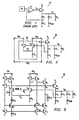
- Figure 1 shows a simplified block diagram of a typical prior art PMOS LDO circuit 10.
- the pass element is MOS transistor M 1 , which is driven by amplifier A 1 .
- the amplifier receives the voltage generated by an internal voltage reference VR 1 , and the voltage produced by a voltage divider network R 1 -R 2 .
- the circuit 10 is connected so that the amplifier achieves equilibrium when the voltage on the tap T of the voltage divider equals the voltage generated by the reference VR 1 .
- the micropower LDO architecture contains multiple poles at relatively low frequencies, and therefore requires the insertion of compensating zeros to boost the phase, or otherwise the phase margin will deteriorate to the point that the circuit becomes unstable. These zeros are difficult to generate using integrated components because they must lie at relatively low frequencies (10-100kHz), they must not use large amounts of die area, and they must not consume any current. There are two basic techniques that have been used to insert zeros in this type of LDO architecture:
- US 5,982,226 describes a low drop-out regulator including an error amplifier with a first input for receiving a reference voltage, a second input and an output, a pass element having a control terminal coupled to the output of the error amplifier and a current path coupled between an input voltage and an output terminal.
- the error amplifier provides an added pole/zero pair in the frequency response of the regulator.
- US 5,982,226 does not mention a Brokaw cell.
- US 4,789,819 relates to a voltage reference circuit including a Brokaw cell band-gap reference circuit with breakpoint compensation to adjust the temperature coefficient of the reference voltage provided by the Brokaw cell as a function of temperature.
- US 4,789,819 is silent with regard to a pole/zero pair in the Brokaw cell.
- the present invention achieves technical advantages as a micropower low-dropout voltage regulator having a shunt capacitor at the counterphase input of a Brokaw transconductance cell including a base current compensation resistor.
- This resistor and capacitor provides a zero frequency that does not depend upon the attenuation ratio of the feedback divider.
- the counterphase compensation capacitor provides a low-frequency zero using a reasonably sized capacitor, providing a pole-zero separation that does not depend upon the attenuator ratio, and which requires no additional current-consuming components.
- the present invention can be combined with both feedback bypass compensation and ESR compensation to provide a wide-range phase boost capable of compensating a micropower LDO based upon the Brokaw transconductance cell.
- the configuration can be generally applied to any amplifier based on the Brokaw cell.
- a voltage regulator produces an output signal and has a Brokaw cell comprising a first transistor and a second transistor.
- a compensation circuit is coupled to the Brokaw cell and generates a pole-zero pair in the Brokaw cell.
- Each of the first and second transistors have a base, wherein the compensation circuit comprises a base-current compensating resistor coupled between the first and second transistor bases.
- the compensation circuit also comprises a capacitor coupled to the compensating resistor.
- the first and second transistors operate in counterphase to generate respective output signals 180° out-of-phase to one another.
- the compensation circuit is configured to provide a phase boost approaching 90° and which is independent of the output signal of the voltage regulator.
- the compensation circuit is configured to compensate the voltage regulator even when the regulator has a low feedback attenuation ratio.
- the pole-zero pair defines a pole-zero separation, wherein the pole-zero separation is independent of attenuation ratio of the voltage regulator.
- the compensation circuit can be combined with a feedback bypass compensation circuit and an ESR compensation circuit to provide a wide-range phase boost.
- the Brokaw cell is configured as an operational transconductance amplifier (OTA).
- OTA operational transconductance amplifier
- FIG. 1 shows the basic topology of such a circuit 20.
- the Brokaw transconductance cell consists of bipolar transistors Q 1 and Q 2 and resistors R 3 and R 4 , shown at 22.
- the emitter area of transistor Q 1 is an integer multiple N of the emitter area of transistor Q 2 .
- V bg V be ⁇ 2 + 2 ⁇ V T ⁇ R ⁇ 4 R ⁇ 3 ⁇ l ⁇ n N
- the OTA described above acts both as its own reference and as an amplifier, so it replaces components VR 1 and A 1 in Figure 1.
- Figure 2 shows how a complete LDO could be implemented around the OTA.
- This circuit has a very small number of current paths (five in all, four in the OTA and one in the resistor divider R 3 and R 4 ), making it a candidate for a micropower LDO.
- circuit 30 shows a practical implementation of a micropower LDO.
- Current mirrors CM 1 and CM 2 have been implemented as PNP transistors Q 3 -Q 4 and transistors Q 5 -Q 6 .
- Current mirror CM 3 has been implemented as NPN transistors Q 9 -Q 10 with a MOS beta helper transistor M 2 biased by diode-connected transistor Q 12 .
- a current limiting component I 1 typically a depletion-mode MOS transistor
- I 1 typically a depletion-mode MOS transistor
- transistor M 1 In order to minimize the impedance at node Vp, it is traditional to insert a follower stage, in this case consisting of emitter follower transistor Q 8 biased by a limb of the lower current mirror based on transistor Q 11 . In order to obtain adequate headroom for transistor Q 8 , transistor M 1 must have a high threshold voltage (V t > 1V). This arrangement doesn't necessarily reduce the impedance at node V p as much as desired because the output impedance of transistor Q 8 depends inversely upon its emitter current, and low currents therefore prevent one from taking full advantage of transistor Q 8 . However, this stage is still necessary in order to allow proper implementation of a startup circuit, as will be explained below.
- the OTA must have a relatively high output impedance. This is achieved in part by adding a cascode transistor M 3 to the output limb of the lower current mirror CM 3 .
- This transistor can be biased from beta helper transistor M 1 due to the addition of diode transistor Q 12 , which ensures that the current through transistors M 1 and M 2 have a definite relationship to one another (as would not be the case if this diode were omitted).
- a cascode on transistor Q 6 could provide a higher output impedance, but only at the price of degrading the already-minimal headroom of transistor Q 8 .
- Figure 3 shows a better solution, consisting of a backside-cascode transistor Q 7 which holds the collector of transistor Q 4 at virtually the same voltage as the collector of transistor Q 6 , thus eliminating most of the output voltage variations that low gain would otherwise produce.
- the OTA circuit 30 of Figure 3 has a secondary equilibrium point at zero bias.
- a small current source I 2 has been added which pulls down on the gate of transistor M 1 to begin start-up.
- I 2 could be a depletion-mode transistor.
- an isolation stage must be inserted between the output of the OTA and node Vp; in this circuit emitter follower transistor Q 8 performs this function.
- Transistor M 4 has been added to balance the limbs of mirror CM 3 , but is not absolutely necessary.
- LDO voltage regulators are notoriously difficult to compensate.
- the typical LDO ( Figure 1 ) is dominated by two poles: a load pole formed by the load capacitance C L , and a gate pole formed by the gate capacitance of transistor M 1 looking into the output impedance of amplifier A 1 .
- the extremely low currents used in the amplifier cause it to exhibit a very high output impedance.
- R o V T I o which for a typical bias current I 0 of 0.5 ⁇ A gives an output impedance of 52k ⁇ .
- This pole can move through a wide range of frequencies, depending upon the load resistance R L .
- the stability becomes poorest for the lowest R L (in other words, at the highest currents).
- f L moves out to a higher frequency and approaches (or even exceeds) the frequency of the gate pole.
- R L 30 ⁇
- C L 1 ⁇ F
- f L 53kHz.
- the two classical techniques of generating lead compensation in LDO's are the insertion of an ESR zero and the insertion of a feedback bypass capacitor.
- the ESR zero capacitor appears in Figure 1 as R esr .
- the feedback bypass capacitor has better possibilities in micropower circuits.
- This capacitor appears in the circuit 30 of Figure 3 as capacitor C 1 .
- the pole-zero separation f p /f z should equal at least 3-5 to obtain good results from this circuit.
- the feedback bypass capacitor doesn't provide much benefit for output voltages below 3V. Unfortunately, it is precisely these voltages that are of greatest importance in modern low-voltage applications. Therefore, the feedback bypass capacitor provides limited benefit. Many low-voltage LDO's still include feedback bypass capacitors because they neutralize the inevitable parasitic poles introduced by parasitic capacitance within the feedback divider.
- the present invention derives technical advantages by adding a capacitor C 2 that generates a pole-zero pair in the Brokaw transconductance cell. This can be explained intuitively as follows:
- the current at the base of transistor Q 8 equals IC 2 -IC 1 , so transistors Q 1 and transistor Q 2 operate in counterphase. In other words, an input to transistor Q 1 will produce an output signal at node Vp 180° out-of-phase to the output signal generated in response to an input to transistor Q 2 . Since a capacitor from the base of transistor Q 2 to ground would behave as a pole (90° phase lag), a capacitor from the base of transistor Q 1 to ground should produce a zero (90° phase lead). Resistor R 5 plays a vital role because it provides isolation between transistors Q 1 and Q 2 and allows the capacitor C 2 to affect only one of the two transistors Q 1 and Q 2 . One would intuitively expect the zero to depend upon resistors R 3 and R 4 , since these lie in the ground path from capacitor C 2 , and one would expect to find a pole dependent upon resistor R 5 .
- resistors R 3 and r e are both considerably smaller than 2R 4 , the zero frequency can be approximated as: f z ⁇ R 3 4 ⁇ ⁇ R 5 ⁇ R 4 ⁇ C 2 and the pole-zero separation f p /f z equals: f p f z ⁇ 2 ⁇ R 4 R 3
- the zero frequency does not depend upon the attenuator ratio, but does depend upon the parallel combination resistance R 1
- a typical micropower regulator might have a parallel resistance R 1
- R 2 1 M ⁇ , and a 5pF compensation capacitor C 2 would provide a zero at 16kHz.
- the counterphase compensation capacitor provides a low-frequency zero using a reasonably sized capacitor C 2 , whose pole-zero separation does not depend upon attenuator ratio, and therefore is independent of output voltage, and which requires no additional current-consuming components.
- This technique can be combined with both feedback bypass compensation and ESR compensation to provide a wide-range phase boost capable of compensating a micropower LDO based upon the Brokaw transconductance cell.
- the illustrated circuit 30 uses an OTA configuration about the transconductance cell, but the technique is more general and can be applied to any amplifier based on the Brokaw cell.
Landscapes
- Engineering & Computer Science (AREA)
- Microelectronics & Electronic Packaging (AREA)
- Physics & Mathematics (AREA)
- Power Engineering (AREA)
- Nonlinear Science (AREA)
- Electromagnetism (AREA)
- General Physics & Mathematics (AREA)
- Radar, Positioning & Navigation (AREA)
- Automation & Control Theory (AREA)
- Amplifiers (AREA)
- Continuous-Control Power Sources That Use Transistors (AREA)
- Dc-Dc Converters (AREA)
Claims (17)
- Régulateur de tension produisant un signal de sortie, comprenant :une cellule de Brokaw qui comprend un premier transistor (Q1) et un deuxième transistor (Q2) etun circuit de compensation (R5, C2) couplé à ladite cellule de Brokaw, qui génère une paire de pôles zéro dans la dite cellule de Brokaw.
- Régulateur de tension selon la revendication 1, dans lequel chacun desdits premier et deuxième transistors (Q1, Q2) présente une base, dans lequel ledit circuit de compensation comprend une première résistance de compensation de courant de base (R5) couplée entre les bases desdits premier et deuxième transistors et un premier condensateur (C2) couplé à ladite résistance de compensation.
- Régulateur de tension selon la revendication 2, dans lequel chaque dit transistor présente un émetteur, comprenant en outre une deuxième résistance (R3) couplée entre les émetteurs desdits premier et deuxième transistors, et une troisième résistance couplée à ladite deuxième résistance (R4) en définissant un circuit diviseur de tension.
- Régulateur de tension selon la revendication 1 ou la revendication 2, dans lequel lesdits premier et deuxième transistors (Q1, Q2) fonctionnent en opposition de phase de façon à générer des signaux de sortie respectifs déphasés de 180° entre eux.
- Régulateur de tension selon la revendication 1, dans lequel ledit circuit de compensation est configuré de façon à fournir une poussée de phase qui s'approche de 90° et qui est indépendante du signal de sortie du régulateur de tension.
- Régulateur de tension selon la revendication 1, dans lequel ledit circuit de compensation est configuré de façon à compenser le régulateur de tension même quand il présente un faible rapport d'atténuation.
- Régulateur de tension selon la revendication 6, dans lequel ledit circuit de compensation est configuré de façon à présenter une fréquence zéro qui est indépendante du rapport d'atténuation.
- Régulateur de tension selon la revendication 1, dans lequel ladite paire de pôles zéro définit une séparation des pôles zéro, dans lequel ladite séparation des pôles zéro est indépendante d'un rapport d'atténuation du régulateur de tension.
- Régulateur de tension selon la revendication 1, comprenant en outre un circuit de compensation en dérivation à rétroaction et un circuit de compensation ESR qui fournissent une poussée de phase à gamme étendue dudit circuit de compensation.
- Régulateur de tension selon la revendication 1 ou la revendication 2, dans lequel ladite cellule de Brokaw comprend une cellule de Brokaw à transconductance.
- Régulateur de tension selon la revendication 2, dans lequel ladite première résistance et ledit premier condensateur produisent une poussée de phase qui s'approche de 90°.
- Régulateur de tension selon la revendication 11, dans lequel ladite poussée de phase est indépendante du signal de sortie du régulateur de tension.
- Régulateur de tension selon la revendication 2, dans lequel ledit régulateur de tension présente un rapport d'atténuation, dans lequel ladite première résistance (R5) et ledit premier condensateur (C2) fournissent une fréquence zéro qui est indépendante du rapport d'atténuation.
- Régulateur de tension selon la revendication 13, comprenant en outre des circuits de compensation qui génèrent une fréquence de pôle, dans lequel ladite fréquence zéro et ladite fréquence de pôle définissent une séparation des pôles zéro.
- Régulateur de tension selon la revendication 14, dans lequel ladite séparation des pôles zéro est indépendante du rapport d'atténuation.
- Régulateur de tension selon la revendication 14, dans lequel lesdits circuits de compensation comprennent un circuit de compensation en dérivation à rétroaction et un circuit de compensation ESR qui fournissent une poussée de phase à gamme étendue dudit circuit de compensation.
- Régulateur de tension selon la revendication 2, dans lequel ladite première résistance (R5) et ledit premier condensateur (C2) sont configurés de façon à compenser le régulateur de tension qui présente un faible rapport d'atténuation.
Applications Claiming Priority (2)
| Application Number | Priority Date | Filing Date | Title |
|---|---|---|---|
| US470910 | 1999-12-23 | ||
| US09/470,910 US6259238B1 (en) | 1999-12-23 | 1999-12-23 | Brokaw transconductance operational transconductance amplifier-based micropower low drop out voltage regulator having counterphase compensation |
Publications (2)
| Publication Number | Publication Date |
|---|---|
| EP1111493A1 EP1111493A1 (fr) | 2001-06-27 |
| EP1111493B1 true EP1111493B1 (fr) | 2011-05-25 |
Family
ID=23869553
Family Applications (1)
| Application Number | Title | Priority Date | Filing Date |
|---|---|---|---|
| EP00127218A Expired - Lifetime EP1111493B1 (fr) | 1999-12-23 | 2000-12-14 | Régulateur de tension à faible tension de déchet et faible courant de repos |
Country Status (4)
| Country | Link |
|---|---|
| US (1) | US6259238B1 (fr) |
| EP (1) | EP1111493B1 (fr) |
| JP (1) | JP2001216036A (fr) |
| AT (1) | ATE511134T1 (fr) |
Families Citing this family (27)
| Publication number | Priority date | Publication date | Assignee | Title |
|---|---|---|---|---|
| JP4824228B2 (ja) * | 2001-09-07 | 2011-11-30 | 株式会社リコー | 半導体装置 |
| CN100367489C (zh) * | 2001-09-07 | 2008-02-06 | 株式会社理光 | 半导体器件 |
| US6518737B1 (en) * | 2001-09-28 | 2003-02-11 | Catalyst Semiconductor, Inc. | Low dropout voltage regulator with non-miller frequency compensation |
| US6522112B1 (en) * | 2001-11-08 | 2003-02-18 | National Semiconductor Corporation | Linear regulator compensation inversion |
| US6861827B1 (en) * | 2003-09-17 | 2005-03-01 | System General Corp. | Low drop-out voltage regulator and an adaptive frequency compensation |
| US6975099B2 (en) | 2004-02-27 | 2005-12-13 | Texas Instruments Incorporated | Efficient frequency compensation for linear voltage regulators |
| US7564225B2 (en) * | 2005-09-28 | 2009-07-21 | Monolithic Power Systems, Inc. | Low-power voltage reference |
| JP2008117176A (ja) * | 2006-11-06 | 2008-05-22 | Seiko Instruments Inc | 電圧制御回路 |
| US7612613B2 (en) * | 2008-02-05 | 2009-11-03 | Freescale Semiconductor, Inc. | Self regulating biasing circuit |
| EP2151732B1 (fr) * | 2008-08-08 | 2012-10-17 | CSEM Centre Suisse d'Electronique et de Microtechnique SA - Recherche et Développement | Régulateur stable à faible chute de tension |
| US7755382B2 (en) * | 2008-08-22 | 2010-07-13 | Semiconductor Components Industries, L.L.C. | Current limited voltage supply |
| US20100066326A1 (en) * | 2008-09-16 | 2010-03-18 | Huang Hao-Chen | Power regulator |
| US7733180B1 (en) * | 2008-11-26 | 2010-06-08 | Texas Instruments Incorporated | Amplifier for driving external capacitive loads |
| JP4853511B2 (ja) * | 2008-12-04 | 2012-01-11 | 株式会社デンソー | スイッチング電源回路 |
| CN101777878B (zh) * | 2009-12-29 | 2012-10-03 | 北京衡天北斗科技有限公司 | 用于输出宽频带大电流的功率放大器 |
| US8188719B2 (en) * | 2010-05-28 | 2012-05-29 | Seiko Instruments Inc. | Voltage regulator |
| WO2012003597A1 (fr) * | 2010-07-05 | 2012-01-12 | St-Ericsson Sa | Circuit régulateur de tension |
| US9595929B2 (en) | 2013-10-11 | 2017-03-14 | Texas Instruments Incorporated | Distributed pole-zero compensation for an amplifier |
| CN105573395B (zh) * | 2015-11-04 | 2017-08-22 | 深圳市芯海科技有限公司 | 一种非外置电容的低压差线性稳压电路 |
| TWI674493B (zh) * | 2018-05-25 | 2019-10-11 | 新加坡商光寶科技新加坡私人有限公司 | 低壓降分流穩壓器 |
| US10444780B1 (en) * | 2018-09-20 | 2019-10-15 | Qualcomm Incorporated | Regulation/bypass automation for LDO with multiple supply voltages |
| US10591938B1 (en) | 2018-10-16 | 2020-03-17 | Qualcomm Incorporated | PMOS-output LDO with full spectrum PSR |
| US10756676B2 (en) | 2018-10-17 | 2020-08-25 | Analog Devices Global Unlimited Company | Amplifier systems for driving a wide range of loads |
| WO2022019969A1 (fr) | 2020-07-24 | 2022-01-27 | Qualcomm Incorporated | Régulateur à faible perte de niveau basé sur une pompe de charge |
| CN112486239B (zh) * | 2020-12-25 | 2022-04-08 | 北京集创北方科技股份有限公司 | 一种低压差线性稳压器电路 |
| CN113110685B (zh) * | 2021-03-31 | 2022-05-20 | 北京奥创在线科技有限公司 | 用于高压电路的高精度低压偏置产生电路 |
| CN115268541B (zh) * | 2022-05-11 | 2023-07-07 | 南京邮电大学 | 用于数字低压差线性稳压器的模拟相位补偿系统 |
Family Cites Families (11)
| Publication number | Priority date | Publication date | Assignee | Title |
|---|---|---|---|---|
| US4458212A (en) * | 1981-12-30 | 1984-07-03 | Mostek Corporation | Compensated amplifier having pole zero tracking |
| US4710728A (en) * | 1986-06-30 | 1987-12-01 | Motorola, Inc. | Amplifier having improved gain-bandwidth product |
| US4789819A (en) * | 1986-11-18 | 1988-12-06 | Linear Technology Corporation | Breakpoint compensation and thermal limit circuit |
| US4851953A (en) * | 1987-10-28 | 1989-07-25 | Linear Technology Corporation | Low voltage current limit loop |
| US4792745A (en) * | 1987-10-28 | 1988-12-20 | Linear Technology Corporation | Dual transistor output stage |
| US4902959A (en) * | 1989-06-08 | 1990-02-20 | Analog Devices, Incorporated | Band-gap voltage reference with independently trimmable TC and output |
| US5325070A (en) * | 1993-01-25 | 1994-06-28 | Motorola, Inc. | Stabilization circuit and method for second order tunable active filters |
| US5672962A (en) * | 1994-12-05 | 1997-09-30 | Texas Instruments Incorporated | Frequency compensated current output circuit with increased gain |
| US5686821A (en) * | 1996-05-09 | 1997-11-11 | Analog Devices, Inc. | Stable low dropout voltage regulator controller |
| US5774021A (en) * | 1996-10-03 | 1998-06-30 | Analog Devices, Inc. | Merged transconductance amplifier |
| US5982226A (en) * | 1997-04-07 | 1999-11-09 | Texas Instruments Incorporated | Optimized frequency shaping circuit topologies for LDOs |
-
1999
- 1999-12-23 US US09/470,910 patent/US6259238B1/en not_active Expired - Lifetime
-
2000
- 2000-12-14 EP EP00127218A patent/EP1111493B1/fr not_active Expired - Lifetime
- 2000-12-14 AT AT00127218T patent/ATE511134T1/de not_active IP Right Cessation
- 2000-12-22 JP JP2000390362A patent/JP2001216036A/ja not_active Abandoned
Also Published As
| Publication number | Publication date |
|---|---|
| ATE511134T1 (de) | 2011-06-15 |
| JP2001216036A (ja) | 2001-08-10 |
| EP1111493A1 (fr) | 2001-06-27 |
| US6259238B1 (en) | 2001-07-10 |
Similar Documents
| Publication | Publication Date | Title |
|---|---|---|
| EP1111493B1 (fr) | Régulateur de tension à faible tension de déchet et faible courant de repos | |
| EP1769301B1 (fr) | Circuit de tension proportionnel a la temperature absolue | |
| US8115463B2 (en) | Compensation of LDO regulator using parallel signal path with fractional frequency response | |
| EP1569062B1 (fr) | Compensation de fréquence efficace pour régulateur de tension linéaire. | |
| US6465994B1 (en) | Low dropout voltage regulator with variable bandwidth based on load current | |
| EP0911978B1 (fr) | Génération de tensions de références symétriques à faible bruit et compensées en température | |
| US4626770A (en) | NPN band gap voltage reference | |
| US6249112B1 (en) | Voltage regulating circuit for a capacitive load | |
| EP1635239A1 (fr) | Polarisation adaptif pour un régulateur de voltage a alimentation en mode de courant | |
| US20040004468A1 (en) | LDO regulator with wide output load range and fast internal loop | |
| EP0620515B1 (fr) | Source de tension de référence du type Bandgap | |
| US20200125126A1 (en) | Voltage regulator circuit with high power supply rejection ratio | |
| GB2223608A (en) | A stabilized low dropout voltage regulator circuit | |
| EP1229420B1 (fr) | Référence de tension du type bande interdite à basse tension d'alimentation | |
| US6522114B1 (en) | Noise reduction architecture for low dropout voltage regulators | |
| CN113359918B (zh) | 一种可输出低噪声和高psrr的ldo电路 | |
| EP3514653B1 (fr) | Circuit de génération de signal | |
| US6791390B2 (en) | Method of forming a voltage regulator semiconductor device having feedback and structure therefor | |
| US5157322A (en) | PNP transistor base drive compensation circuit | |
| EP2804067B1 (fr) | Régulateur de tension LDO à faible puissance et bruit de sortie à faible densité | |
| CN110825157B (zh) | 基于重载补偿的低压差线性稳压器 | |
| DE19818464A1 (de) | Referenzspannung-Erzeugungsschaltung | |
| US4441070A (en) | Voltage regulator circuit with supply voltage ripple rejection to transient spikes | |
| DE3877093T2 (de) | Gesteuerter praezisionsstromgenerator. | |
| US5132559A (en) | Circuit for trimming input offset voltage utilizing variable resistors |
Legal Events
| Date | Code | Title | Description |
|---|---|---|---|
| PUAI | Public reference made under article 153(3) epc to a published international application that has entered the european phase |
Free format text: ORIGINAL CODE: 0009012 |
|
| AK | Designated contracting states |
Kind code of ref document: A1 Designated state(s): AT BE CH CY DE DK ES FI FR GB GR IE IT LI LU MC NL PT SE TR |
|
| AX | Request for extension of the european patent |
Free format text: AL;LT;LV;MK;RO;SI |
|
| 17P | Request for examination filed |
Effective date: 20011210 |
|
| AKX | Designation fees paid |
Free format text: AT BE CH CY DE DK ES FI FR GB GR IE IT LI LU MC NL PT SE TR |
|
| 17Q | First examination report despatched |
Effective date: 20050209 |
|
| GRAP | Despatch of communication of intention to grant a patent |
Free format text: ORIGINAL CODE: EPIDOSNIGR1 |
|
| GRAS | Grant fee paid |
Free format text: ORIGINAL CODE: EPIDOSNIGR3 |
|
| GRAA | (expected) grant |
Free format text: ORIGINAL CODE: 0009210 |
|
| AK | Designated contracting states |
Kind code of ref document: B1 Designated state(s): AT BE CH CY DE DK ES FI FR GB GR IE IT LI LU MC NL PT SE TR |
|
| REG | Reference to a national code |
Ref country code: GB Ref legal event code: FG4D |
|
| REG | Reference to a national code |
Ref country code: CH Ref legal event code: EP |
|
| REG | Reference to a national code |
Ref country code: IE Ref legal event code: FG4D |
|
| REG | Reference to a national code |
Ref country code: DE Ref legal event code: R096 Ref document number: 60046003 Country of ref document: DE Effective date: 20110707 |
|
| REG | Reference to a national code |
Ref country code: NL Ref legal event code: T3 |
|
| PG25 | Lapsed in a contracting state [announced via postgrant information from national office to epo] |
Ref country code: SE Free format text: LAPSE BECAUSE OF FAILURE TO SUBMIT A TRANSLATION OF THE DESCRIPTION OR TO PAY THE FEE WITHIN THE PRESCRIBED TIME-LIMIT Effective date: 20110525 Ref country code: PT Free format text: LAPSE BECAUSE OF FAILURE TO SUBMIT A TRANSLATION OF THE DESCRIPTION OR TO PAY THE FEE WITHIN THE PRESCRIBED TIME-LIMIT Effective date: 20110926 |
|
| PG25 | Lapsed in a contracting state [announced via postgrant information from national office to epo] |
Ref country code: GR Free format text: LAPSE BECAUSE OF FAILURE TO SUBMIT A TRANSLATION OF THE DESCRIPTION OR TO PAY THE FEE WITHIN THE PRESCRIBED TIME-LIMIT Effective date: 20110826 Ref country code: AT Free format text: LAPSE BECAUSE OF FAILURE TO SUBMIT A TRANSLATION OF THE DESCRIPTION OR TO PAY THE FEE WITHIN THE PRESCRIBED TIME-LIMIT Effective date: 20110525 Ref country code: ES Free format text: LAPSE BECAUSE OF FAILURE TO SUBMIT A TRANSLATION OF THE DESCRIPTION OR TO PAY THE FEE WITHIN THE PRESCRIBED TIME-LIMIT Effective date: 20110905 Ref country code: BE Free format text: LAPSE BECAUSE OF FAILURE TO SUBMIT A TRANSLATION OF THE DESCRIPTION OR TO PAY THE FEE WITHIN THE PRESCRIBED TIME-LIMIT Effective date: 20110525 Ref country code: CY Free format text: LAPSE BECAUSE OF FAILURE TO SUBMIT A TRANSLATION OF THE DESCRIPTION OR TO PAY THE FEE WITHIN THE PRESCRIBED TIME-LIMIT Effective date: 20110525 Ref country code: FI Free format text: LAPSE BECAUSE OF FAILURE TO SUBMIT A TRANSLATION OF THE DESCRIPTION OR TO PAY THE FEE WITHIN THE PRESCRIBED TIME-LIMIT Effective date: 20110525 |
|
| PG25 | Lapsed in a contracting state [announced via postgrant information from national office to epo] |
Ref country code: DK Free format text: LAPSE BECAUSE OF FAILURE TO SUBMIT A TRANSLATION OF THE DESCRIPTION OR TO PAY THE FEE WITHIN THE PRESCRIBED TIME-LIMIT Effective date: 20110525 |
|
| PLBE | No opposition filed within time limit |
Free format text: ORIGINAL CODE: 0009261 |
|
| STAA | Information on the status of an ep patent application or granted ep patent |
Free format text: STATUS: NO OPPOSITION FILED WITHIN TIME LIMIT |
|
| 26N | No opposition filed |
Effective date: 20120228 |
|
| PG25 | Lapsed in a contracting state [announced via postgrant information from national office to epo] |
Ref country code: IT Free format text: LAPSE BECAUSE OF FAILURE TO SUBMIT A TRANSLATION OF THE DESCRIPTION OR TO PAY THE FEE WITHIN THE PRESCRIBED TIME-LIMIT Effective date: 20110525 |
|
| REG | Reference to a national code |
Ref country code: DE Ref legal event code: R097 Ref document number: 60046003 Country of ref document: DE Effective date: 20120228 |
|
| PG25 | Lapsed in a contracting state [announced via postgrant information from national office to epo] |
Ref country code: MC Free format text: LAPSE BECAUSE OF NON-PAYMENT OF DUE FEES Effective date: 20111231 |
|
| REG | Reference to a national code |
Ref country code: CH Ref legal event code: PL |
|
| PG25 | Lapsed in a contracting state [announced via postgrant information from national office to epo] |
Ref country code: CH Free format text: LAPSE BECAUSE OF NON-PAYMENT OF DUE FEES Effective date: 20111231 Ref country code: LI Free format text: LAPSE BECAUSE OF NON-PAYMENT OF DUE FEES Effective date: 20111231 |
|
| PG25 | Lapsed in a contracting state [announced via postgrant information from national office to epo] |
Ref country code: LU Free format text: LAPSE BECAUSE OF NON-PAYMENT OF DUE FEES Effective date: 20111214 |
|
| PG25 | Lapsed in a contracting state [announced via postgrant information from national office to epo] |
Ref country code: TR Free format text: LAPSE BECAUSE OF FAILURE TO SUBMIT A TRANSLATION OF THE DESCRIPTION OR TO PAY THE FEE WITHIN THE PRESCRIBED TIME-LIMIT Effective date: 20110525 |
|
| REG | Reference to a national code |
Ref country code: FR Ref legal event code: PLFP Year of fee payment: 16 |
|
| PGFP | Annual fee paid to national office [announced via postgrant information from national office to epo] |
Ref country code: IE Payment date: 20151125 Year of fee payment: 16 Ref country code: GB Payment date: 20151125 Year of fee payment: 16 |
|
| PGFP | Annual fee paid to national office [announced via postgrant information from national office to epo] |
Ref country code: FR Payment date: 20151124 Year of fee payment: 16 Ref country code: NL Payment date: 20151207 Year of fee payment: 16 |
|
| PGFP | Annual fee paid to national office [announced via postgrant information from national office to epo] |
Ref country code: DE Payment date: 20151230 Year of fee payment: 16 |
|
| REG | Reference to a national code |
Ref country code: DE Ref legal event code: R119 Ref document number: 60046003 Country of ref document: DE |
|
| REG | Reference to a national code |
Ref country code: NL Ref legal event code: MM Effective date: 20170101 |
|
| GBPC | Gb: european patent ceased through non-payment of renewal fee |
Effective date: 20161214 |
|
| PG25 | Lapsed in a contracting state [announced via postgrant information from national office to epo] |
Ref country code: NL Free format text: LAPSE BECAUSE OF NON-PAYMENT OF DUE FEES Effective date: 20170101 |
|
| REG | Reference to a national code |
Ref country code: FR Ref legal event code: ST Effective date: 20170831 |
|
| REG | Reference to a national code |
Ref country code: IE Ref legal event code: MM4A |
|
| PG25 | Lapsed in a contracting state [announced via postgrant information from national office to epo] |
Ref country code: FR Free format text: LAPSE BECAUSE OF NON-PAYMENT OF DUE FEES Effective date: 20170102 |
|
| PG25 | Lapsed in a contracting state [announced via postgrant information from national office to epo] |
Ref country code: GB Free format text: LAPSE BECAUSE OF NON-PAYMENT OF DUE FEES Effective date: 20161214 Ref country code: DE Free format text: LAPSE BECAUSE OF NON-PAYMENT OF DUE FEES Effective date: 20170701 Ref country code: IE Free format text: LAPSE BECAUSE OF NON-PAYMENT OF DUE FEES Effective date: 20161214 |