EP1111792A2 - Spannungsgesteuerter Oszillator mit programmierbarer Ausgangsleistung - Google Patents
Spannungsgesteuerter Oszillator mit programmierbarer Ausgangsleistung Download PDFInfo
- Publication number
- EP1111792A2 EP1111792A2 EP00310659A EP00310659A EP1111792A2 EP 1111792 A2 EP1111792 A2 EP 1111792A2 EP 00310659 A EP00310659 A EP 00310659A EP 00310659 A EP00310659 A EP 00310659A EP 1111792 A2 EP1111792 A2 EP 1111792A2
- Authority
- EP
- European Patent Office
- Prior art keywords
- voltage controlled
- controlled oscillator
- signal
- output power
- output
- Prior art date
- Legal status (The legal status is an assumption and is not a legal conclusion. Google has not performed a legal analysis and makes no representation as to the accuracy of the status listed.)
- Withdrawn
Links
Images
Classifications
-
- H—ELECTRICITY
- H03—ELECTRONIC CIRCUITRY
- H03L—AUTOMATIC CONTROL, STARTING, SYNCHRONISATION OR STABILISATION OF GENERATORS OF ELECTRONIC OSCILLATIONS OR PULSES
- H03L7/00—Automatic control of frequency or phase; Synchronisation
- H03L7/06—Automatic control of frequency or phase; Synchronisation using a reference signal applied to a frequency- or phase-locked loop
- H03L7/08—Details of the phase-locked loop
- H03L7/0802—Details of the phase-locked loop the loop being adapted for reducing power consumption
-
- H—ELECTRICITY
- H03—ELECTRONIC CIRCUITRY
- H03L—AUTOMATIC CONTROL, STARTING, SYNCHRONISATION OR STABILISATION OF GENERATORS OF ELECTRONIC OSCILLATIONS OR PULSES
- H03L5/00—Automatic control of voltage, current, or power
-
- H—ELECTRICITY
- H03—ELECTRONIC CIRCUITRY
- H03L—AUTOMATIC CONTROL, STARTING, SYNCHRONISATION OR STABILISATION OF GENERATORS OF ELECTRONIC OSCILLATIONS OR PULSES
- H03L7/00—Automatic control of frequency or phase; Synchronisation
- H03L7/06—Automatic control of frequency or phase; Synchronisation using a reference signal applied to a frequency- or phase-locked loop
- H03L7/08—Details of the phase-locked loop
- H03L7/099—Details of the phase-locked loop concerning mainly the controlled oscillator of the loop
-
- H—ELECTRICITY
- H03—ELECTRONIC CIRCUITRY
- H03L—AUTOMATIC CONTROL, STARTING, SYNCHRONISATION OR STABILISATION OF GENERATORS OF ELECTRONIC OSCILLATIONS OR PULSES
- H03L7/00—Automatic control of frequency or phase; Synchronisation
- H03L7/06—Automatic control of frequency or phase; Synchronisation using a reference signal applied to a frequency- or phase-locked loop
- H03L7/16—Indirect frequency synthesis, i.e. generating a desired one of a number of predetermined frequencies using a frequency- or phase-locked loop
- H03L7/18—Indirect frequency synthesis, i.e. generating a desired one of a number of predetermined frequencies using a frequency- or phase-locked loop using a frequency divider or counter in the loop
Definitions
- the present invention relates to voltage controlled oscillators, and more specifically it relates to regulation of the output signal level from voltage controlled oscillators, when used in different applications, further the invention relates to a method for reducing losses in phase locked loops using voltage controlled oscillators.
- Voltage controlled oscillators are widely used in generating various frequencies within a specified frequency band.
- the voltage controlled oscillator is incorporated in a phase locked loop.
- phase locked loop may incorporate a reference oscillator, a phase detector, a low pass filter, a programmable divider and a voltage controlled oscillator, all co-operating in the following manner.
- the reference oscillator typically a crystal oscillator, generates a fixed frequency which is supplied to the phase detector on a first line.
- the phase detector compares the phase of the signal on the first line with the phase of a frequency signal on a second line originating from the voltage controlled oscillator.
- This frequency signal from the voltage controlled oscillator may be divided down by a programmable divider before the phase comparison in the phase detector takes place.
- the phase detector Based on the comparison the phase detector generates a error signal on a third line, via which it is input to the voltage controlled oscillator.
- the error signal is in the form of a control voltage signal for the voltage controlled oscillator.
- the voltage controlled oscillator Based on the control voltage signal the voltage controlled oscillator generates an output signal on an output line. This signal is at a different frequency from the fixed frequency, depending on the division ratio of the programmable divider.
- the operating frequency When using a voltage controlled oscillator in a phase locked loop in modern mobile communications the operating frequency will typically be in the vicinity of 4 GHz. This signal may then conveniently be divided down with integer factors of 2, 4 and 8, thereby achieving frequencies in the most commonly used frequency bands around 1800 MHz, 1900 MHz, 900 MHz and 450 MHz.
- Increasing the output power of the voltage controlled oscillator may in some cases be a way around this problem.
- programmable dividers for the use at 4 GHz are generally sensitive to too powerful signals.
- the voltage controlled oscillator Since the voltage controlled oscillator is to be used in different mobile telephone constructions where it has to be ensured both that there is sufficient signal and that the signal is not too powerful, the output power has to be adjusted to the actual application.
- the object of the present invention is to provide a voltage controlled oscillator, which may be used in a variety of applications, yet does not suffer from the above drawbacks.
- this object is achieved with a voltage controlled oscillator according to the opening paragraph, wherein said voltage controlled oscillator assembly comprises means for regulating the output power from the at least one voltage controlled oscillator.
- a further object of the invention is to reduce losses when using a voltage controlled oscillator in a phase locked loop.
- this object is achieved with a method for reducing losses in a phase locked loop, wherein a micro-controller arranged on the same chip as the voltage controlled oscillator is used for regulating the level of the output signal from the voltage controlled oscillator chip.
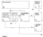
- fig. 1 a phase locked loop incorporating a voltage controlled oscillator assembly 3 according to the invention.
- the phase locked loop incorporates a reference oscillator 2, a phase detector 5, a low pass filter 6, a programmable divider 4 and a voltage controlled oscillator assembly 3 comprising at least one voltage controlled oscillator 14.
- the reference oscillator 2 typically a crystal oscillator, generates a fixed frequency which is supplied to the phase detector 5 on a first line 10.
- the phase detector 5 compares the phase of the signal on the first line 10 with the phase of a frequency signal on a second line 11 originating from the voltage controlled oscillator. This frequency signal from the voltage controlled oscillator may be divided down by the programmable divider 4 before the phase comparison in the phase detector 5 takes place. Based on the comparison the phase detector 5 generates a error signal on a third line 7, via which it is input to the voltage controlled oscillator 14.
- the error signal is in the form of a control voltage signal for the voltage controlled oscillator 14. Based on the control voltage signal the voltage controlled oscillator 14 generates an output signal on an output line 13. This signal is at a different frequency from the fixed frequency, depending on the division ratio of the programmable divider 4.
- the actual signal of interest is tapped via a line 12.
- a second divider (not shown) used to divide the signal of interest down to a frequency desired for a specific use.
- the line 13 connects the output of the voltage controlled oscillator assembly 3 directly to the programmable divider 4, without any intermediate stages such as attenuators.
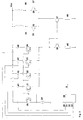
- FIG. 2 In fig. 2 is shown a simplified circuit diagram of an embodiment of the output stage of a VCO according to the invention.
- Two output transistors 35 and 37 are biased by a current mirror comprising two transistors 27 and 28.
- the differential oscillator signal (not shown) is fed to the two input terminals 35 and 37, the differential output signal is available at two output terminals 34 and 36.
- a current multiplier sets the current in the current mirror. Said current multiplier operates as follows:
- a current source 38 sets the current in MOSFET (Metal Oxide Semiconductor Field Effect Transistor) 20.
- MOSFET Metal Oxide Semiconductor Field Effect Transistor
- Another MOSFET 21 is identical to MOSFET 20, thus the currents in the two MOSFETS 21, 22 are the same.
- MOSFET 22 is chosen, so that for a given gate-source voltage, the current is two times the current through the MOSFET 20 with the same gate - source voltage.
- a MOSFET 23 is chosen so that the current for a given gate - source voltage is 4 times that of the MOSFET 20, and a MOSFET 24 is chosen so that the current for a given gate -source voltage is 8 times that of the MOSFET 20.
- MOSFETs 21 - 24 can be switched in and out of the circuit by four switches 41 - 44.
- the switches 41 - 44 are controlled by digital circuit 38 comprising a memory and a bus interface circuit capable of receiving information from e.g. a micro-controller.
- the regulated output on the line 13 need not be derived directly from the voltage controlled oscillator itself, but via an amplifier or buffer associated with the voltage controlled oscillator within the voltage controlled oscillator assembly 3. i.e. on the same chip. In this case the regulation may be effected by regulating the amplification of the amplifier.
- the assembly incorporates a micro-controller 16 which as an external connection which may be connected to an external bus 8. Via this external bus 8 the micro-controller 16 receives information about the output level required for the specific circuit configuration in which the voltage controlled oscillator assembly is placed.
- the voltage controlled oscillator assembly 3 is thus digitally programmable to deliver a specific output level.
- the bus 8 used could for instance be the same bus 8 as used for transmitting the division ratio to the programmable divider.
- the invention facilitates the use of the same integrated circuit containing the voltage controlled oscillator assembly 3, in a wide range of different circuits, because it is of less importance to adapt the layout and properties of these circuits to match the voltage controlled oscillator assembly.
Landscapes
- Stabilization Of Oscillater, Synchronisation, Frequency Synthesizers (AREA)
- Inductance-Capacitance Distribution Constants And Capacitance-Resistance Oscillators (AREA)
- Oscillators With Electromechanical Resonators (AREA)
Applications Claiming Priority (2)
| Application Number | Priority Date | Filing Date | Title |
|---|---|---|---|
| GB9930241A GB2357643A (en) | 1999-12-21 | 1999-12-21 | A mobile phone VCO with controlled output power level |
| GB9930241 | 1999-12-21 |
Publications (2)
| Publication Number | Publication Date |
|---|---|
| EP1111792A2 true EP1111792A2 (de) | 2001-06-27 |
| EP1111792A3 EP1111792A3 (de) | 2002-10-09 |
Family
ID=10866774
Family Applications (1)
| Application Number | Title | Priority Date | Filing Date |
|---|---|---|---|
| EP00310659A Withdrawn EP1111792A3 (de) | 1999-12-21 | 2000-11-30 | Spannungsgesteuerter Oszillator mit programmierbarer Ausgangsleistung |
Country Status (3)
| Country | Link |
|---|---|
| US (1) | US6714091B2 (de) |
| EP (1) | EP1111792A3 (de) |
| GB (1) | GB2357643A (de) |
Families Citing this family (7)
| Publication number | Priority date | Publication date | Assignee | Title |
|---|---|---|---|---|
| US6777885B2 (en) * | 2001-10-12 | 2004-08-17 | Semiconductor Energy Laboratory Co., Ltd. | Drive circuit, display device using the drive circuit and electronic apparatus using the display device |
| US7742064B2 (en) * | 2001-10-30 | 2010-06-22 | Semiconductor Energy Laboratory Co., Ltd | Signal line driver circuit, light emitting device and driving method thereof |
| US7576734B2 (en) * | 2001-10-30 | 2009-08-18 | Semiconductor Energy Laboratory Co., Ltd. | Signal line driving circuit, light emitting device, and method for driving the same |
| US7180479B2 (en) | 2001-10-30 | 2007-02-20 | Semiconductor Energy Laboratory Co., Ltd. | Signal line drive circuit and light emitting device and driving method therefor |
| US7193619B2 (en) * | 2001-10-31 | 2007-03-20 | Semiconductor Energy Laboratory Co., Ltd. | Signal line driving circuit and light emitting device |
| US20040203982A1 (en) * | 2002-04-24 | 2004-10-14 | Barak Ilan S. | Controlling output power in cellular telephones |
| EP1585098A4 (de) | 2003-01-17 | 2007-03-21 | Semiconductor Energy Lab | Stromversorgungsschaltung, signalleitungsansteuerung und entsprechendes steuerverfahren sowie lichtemittierende vorrichtung |
Family Cites Families (10)
| Publication number | Priority date | Publication date | Assignee | Title |
|---|---|---|---|---|
| JP2925158B2 (ja) * | 1988-07-29 | 1999-07-28 | 株式会社東芝 | 変調器および送信器 |
| US5175884A (en) * | 1990-06-01 | 1992-12-29 | Motorola, Inc. | Voltage controlled oscillator with current control |
| US5179358A (en) * | 1992-03-04 | 1993-01-12 | Motorola, Inc. | Circuit, counter and frequency synthesizer with adjustable bias current |
| US5748103A (en) * | 1995-11-13 | 1998-05-05 | Vitalcom, Inc. | Two-way TDMA telemetry system with power conservation features |
| KR100224310B1 (ko) * | 1996-12-05 | 1999-10-15 | 정선종 | 씨모스 전압 제어 발진기 |
| FI102228B1 (fi) * | 1997-01-16 | 1998-10-30 | Nokia Mobile Phones Ltd | Oskillaattorin tehonkulutuksen minimointi |
| US5852386A (en) * | 1997-06-02 | 1998-12-22 | Northrop Grumman Corporation | Apparatus and method for microwave field strength stabilization in cell type atomic clocks |
| US6052036A (en) * | 1997-10-31 | 2000-04-18 | Telefonaktiebolaget L M Ericsson | Crystal oscillator with AGC and on-chip tuning |
| WO2000067384A1 (en) * | 1999-04-30 | 2000-11-09 | Micrel, Inc. | Fully integrated all-cmos am transmitter with automatic antenna tuning |
| FR2795100B1 (fr) | 1999-06-16 | 2001-09-14 | Fort James France | Produit de coton hydrophile comportant une face douce et une face grattante |
-
1999
- 1999-12-21 GB GB9930241A patent/GB2357643A/en not_active Withdrawn
-
2000
- 2000-11-30 EP EP00310659A patent/EP1111792A3/de not_active Withdrawn
- 2000-12-19 US US09/739,230 patent/US6714091B2/en not_active Expired - Lifetime
Also Published As
| Publication number | Publication date |
|---|---|
| EP1111792A3 (de) | 2002-10-09 |
| US6714091B2 (en) | 2004-03-30 |
| US20010011928A1 (en) | 2001-08-09 |
| GB9930241D0 (en) | 2000-02-09 |
| GB2357643A (en) | 2001-06-27 |
Similar Documents
| Publication | Publication Date | Title |
|---|---|---|
| US6400231B1 (en) | Numerically controlled variable oscillator | |
| US7015735B2 (en) | Semiconductor integrated circuit having built-in PLL circuit | |
| US7227415B2 (en) | High frequency power amplifier circuit and radio communication system | |
| KR100926908B1 (ko) | 단일 씨모스 기판 상에 단일 칩 무선 랜 및 블루투스 무선장치들을 구성하기 위한 방법 및 시스템 | |
| US6967535B2 (en) | High frequency power amplifier circuit | |
| EP1387486B1 (de) | Verstärkerschaltung und mehrstufige Verstärkerschaltung | |
| US20050176388A1 (en) | Transmitter and wireless communication apparatus using the transmitter | |
| KR20000005825A (ko) | 전력증폭회로와안정화회로를구비하는무선주파수장치와,이러한장치를구비하는이동트랜시버단말기 | |
| US20040232990A1 (en) | Power amplifier module | |
| US6714091B2 (en) | VCO with programmable output power | |
| JP2002261542A (ja) | 発振器及びそれを用いた通信機 | |
| EP0622895B1 (de) | Kommunikationsapparat mit Leistungsverstärker | |
| EP1281237B1 (de) | Frequenzteiler mit veränderbarem teilverhältnis und angepasstem leistungsverbrauch | |
| EP1526638B1 (de) | Verstärker mit variabler Verstärkung | |
| JP4276537B2 (ja) | 基板過渡抑制を備えた高性能集積回路調整器 | |
| JPH11317661A (ja) | 単カウンタ二重係数分周装置 | |
| US20050266820A1 (en) | Selectable pole bias line filter | |
| US20040203982A1 (en) | Controlling output power in cellular telephones | |
| KR100722023B1 (ko) | 발진기 회로, 전압 제어 발진기, 위상 동기 루프, 집적 회로 및 텔레커뮤니케이션 장치 | |
| JP2000196442A (ja) | チャ―ジポンプの出力電流を平衡させる方法とチャ―ジポンプ構成ならびに無線通信装置 | |
| US6590431B1 (en) | Maintaining substantially constant trans-conductance without substantially changing power consumption | |
| JP3786558B2 (ja) | 半導体集積回路及び無線通信機器 | |
| US20090042517A1 (en) | System And Method For Low Noise Output Divider And Buffer Having Low Current Consumption | |
| JP3550115B2 (ja) | アナログ信号伝達回路 | |
| JPS59212035A (ja) | 送信出力制御回路 |
Legal Events
| Date | Code | Title | Description |
|---|---|---|---|
| PUAI | Public reference made under article 153(3) epc to a published international application that has entered the european phase |
Free format text: ORIGINAL CODE: 0009012 |
|
| AK | Designated contracting states |
Kind code of ref document: A2 Designated state(s): AT BE CH CY DE DK ES FI FR GB GR IE IT LI LU MC NL PT SE TR |
|
| AX | Request for extension of the european patent |
Free format text: AL;LT;LV;MK;RO;SI |
|
| RAP1 | Party data changed (applicant data changed or rights of an application transferred) |
Owner name: NOKIA CORPORATION |
|
| PUAL | Search report despatched |
Free format text: ORIGINAL CODE: 0009013 |
|
| RIC1 | Information provided on ipc code assigned before grant |
Free format text: 7H 03L 7/099 A, 7H 03B 5/00 B, 7H 03L 5/00 B |
|
| AK | Designated contracting states |
Kind code of ref document: A3 Designated state(s): AT BE CH CY DE DK ES FI FR GB GR IE IT LI LU MC NL PT SE TR |
|
| AX | Request for extension of the european patent |
Free format text: AL;LT;LV;MK;RO;SI |
|
| 17P | Request for examination filed |
Effective date: 20030409 |
|
| AKX | Designation fees paid |
Designated state(s): AT BE CH CY DE DK ES FI FR GB GR IE IT LI LU MC NL PT SE TR |
|
| 17Q | First examination report despatched |
Effective date: 20030530 |
|
| STAA | Information on the status of an ep patent application or granted ep patent |
Free format text: STATUS: THE APPLICATION IS DEEMED TO BE WITHDRAWN |
|
| 18D | Application deemed to be withdrawn |
Effective date: 20031010 |