EP1111917B1 - Verfahren zur dynamischen Berechnung von Interpolationsphasen in einem Videonormwandler - Google Patents
Verfahren zur dynamischen Berechnung von Interpolationsphasen in einem Videonormwandler Download PDFInfo
- Publication number
- EP1111917B1 EP1111917B1 EP00460071A EP00460071A EP1111917B1 EP 1111917 B1 EP1111917 B1 EP 1111917B1 EP 00460071 A EP00460071 A EP 00460071A EP 00460071 A EP00460071 A EP 00460071A EP 1111917 B1 EP1111917 B1 EP 1111917B1
- Authority
- EP
- European Patent Office
- Prior art keywords
- field
- signal
- memory
- interpolation
- value
- Prior art date
- Legal status (The legal status is an assumption and is not a legal conclusion. Google has not performed a legal analysis and makes no representation as to the accuracy of the status listed.)
- Expired - Lifetime
Links
- 238000000034 method Methods 0.000 title claims description 11
- 230000015654 memory Effects 0.000 claims description 45
- 238000006243 chemical reaction Methods 0.000 claims description 14
- 238000004364 calculation method Methods 0.000 claims description 11
- 230000008569 process Effects 0.000 claims description 10
- 230000006870 function Effects 0.000 claims description 3
- 238000001914 filtration Methods 0.000 description 2
- 230000000750 progressive effect Effects 0.000 description 2
- 230000002123 temporal effect Effects 0.000 description 2
- RRLHMJHRFMHVNM-BQVXCWBNSA-N [(2s,3r,6r)-6-[5-[5-hydroxy-3-(4-hydroxyphenyl)-4-oxochromen-7-yl]oxypentoxy]-2-methyl-3,6-dihydro-2h-pyran-3-yl] acetate Chemical compound C1=C[C@@H](OC(C)=O)[C@H](C)O[C@H]1OCCCCCOC1=CC(O)=C2C(=O)C(C=3C=CC(O)=CC=3)=COC2=C1 RRLHMJHRFMHVNM-BQVXCWBNSA-N 0.000 description 1
- 230000003111 delayed effect Effects 0.000 description 1
- 230000009977 dual effect Effects 0.000 description 1
- 230000004048 modification Effects 0.000 description 1
- 238000012986 modification Methods 0.000 description 1
- 238000003672 processing method Methods 0.000 description 1
- 230000004044 response Effects 0.000 description 1
- 230000001360 synchronised effect Effects 0.000 description 1
- 238000010200 validation analysis Methods 0.000 description 1
Images

Classifications
-
- G—PHYSICS
- G09—EDUCATION; CRYPTOGRAPHY; DISPLAY; ADVERTISING; SEALS
- G09G—ARRANGEMENTS OR CIRCUITS FOR CONTROL OF INDICATING DEVICES USING STATIC MEANS TO PRESENT VARIABLE INFORMATION
- G09G5/00—Control arrangements or circuits for visual indicators common to cathode-ray tube indicators and other visual indicators
- G09G5/003—Details of a display terminal, the details relating to the control arrangement of the display terminal and to the interfaces thereto
- G09G5/006—Details of the interface to the display terminal
-
- H—ELECTRICITY
- H04—ELECTRIC COMMUNICATION TECHNIQUE
- H04N—PICTORIAL COMMUNICATION, e.g. TELEVISION
- H04N7/00—Television systems
- H04N7/01—Conversion of standards, e.g. involving analogue television standards or digital television standards processed at pixel level
- H04N7/0135—Conversion of standards, e.g. involving analogue television standards or digital television standards processed at pixel level involving interpolation processes
-
- G—PHYSICS
- G09—EDUCATION; CRYPTOGRAPHY; DISPLAY; ADVERTISING; SEALS
- G09G—ARRANGEMENTS OR CIRCUITS FOR CONTROL OF INDICATING DEVICES USING STATIC MEANS TO PRESENT VARIABLE INFORMATION
- G09G2340/00—Aspects of display data processing
- G09G2340/04—Changes in size, position or resolution of an image
- G09G2340/0407—Resolution change, inclusive of the use of different resolutions for different screen areas
- G09G2340/0435—Change or adaptation of the frame rate of the video stream
Definitions
- Known frequency conversion devices are utilized, among other things, for standards conversion, for example the conversion of a PAL or SECAM 50Hz signal into an NTSC 60Hz signal. They are also utilized to increase the scanning frequency of television receivers, typically from 50 Hz to 100 Hz, for the purpose of improving the quality of the picture, by reducing the large area flicker.
- the frequency of the signal to be converted and the frequency of the converted signal are known in advance.
- the interpolation process consists in creating intermediate fields between two reference fields of the input signal to be converted. This process is shown diagrammatically in Figure 1.
- the processing methods utilized require knowledge of the interpolation phase for each field to be interpolated.
- the aim of the invention is to alleviate the aforesaid drawbacks.
- the process automatically calculates the interpolation phase corresponding to the output signal to be generated, when the scanning frequency of this output signal is not known a priori.
- the device obtained is compatible with any type of output signal, at least in a wide frequency range.
- the device is simple to implement and cheap. It makes it possible to supply adjustable scanning frequency apparatuses, such as monitors of PC-type personal computers.
- the interpolation is carried out between the field T1 and the field immediately following it T2.
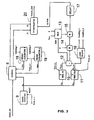
- the second input of the adder originates from the output of the multiplexer 13.
- This signal is transmitted, after passing through a delay circuit 17, to the interpolator 20.
- N CAP. ⁇ P W_FIELD of the memory 8 is finite and the input fields are written thereto cyclically.
- N CAP 4 fields
- the writing of the fifth field will commence at the address 0 and will therefore overwrite the content of the first field.
- P W_OUT becomes less than P W_IN
- the output from the adder 15 corresponds to the value ⁇ calculated at each arrival of the field synchronization signals.
- This coefficient ⁇ is delayed by the delay circuit 17 in such a way as to be able to be applied correctly to the set of fields T1 and T2.
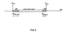
- the previous calculations assume a continuous stream of data of the input video signal.
- the signals include a field blanking interval (VBI standing for Vertical Blanking Interval) during which the field flyback occurs.
- VBI standing for Vertical Blanking Interval
Landscapes
- Engineering & Computer Science (AREA)
- Physics & Mathematics (AREA)
- Computer Hardware Design (AREA)
- General Physics & Mathematics (AREA)
- Theoretical Computer Science (AREA)
- Multimedia (AREA)
- Signal Processing (AREA)
- Television Systems (AREA)
Claims (5)
- Prozeß zur Frequenzumsetzung unter Verwendung einer dynamischen Berechnung der Interpolationsphasen eines Eingangsvideosignals mit einer Frequenz F1, die durch ein Synchronisationssignal S1 definiert wird, zu einem Ausgangsvideosignal mit einer variablen Frequenz-F2, die durch ein Synchronisationssignal S2 definiert wird, mit den folgenden Schritten: Schreiben des Eingangssignals in einen Speicher (8) auf der Basis eines Schreibzeigers PW und Lesen aus dem Speicher, um das Ausgangssignal zu erhalten, dadurch gekennzeichnet, daß er beim Empfang des Synchronisationssignals S1 die Position des Schreibzeigers PW speichert, um so einen Wert PW_IN bereitzustellen, und auch beim Empfang des Synchronisationssignals S2, um so einen Wert PW_OUT bereitzustellen, und daß er dynamisch eine Interpolationsphase α (12, 13, 14, 15) folgendermaßen berechnet:

oder
wobei ΔPW_FIELD die zur Speicherung eines Halbbildes oder Vollbildes des Eingangssignals erforderliche Speichermenge und NCAP die Kapazität des Speichers (8) als Anzahl von Halbbildern oder Vollbildern ausgedrückt ist,
und daß er eine diesem Wert entsprechende Phaseninterpolation (20) durchführt. - Prozeß nach Anspruch 1, dadurch gekennzeichnet, daß drei oder vier sukzessive Halbbilder oder Vollbilder in dem Speicher (8) gespeichert werden und daß die Interpolation an den Halbbildern oder Vollbildern, die denen folgen, die beim Empfang des für die Berechnung der Interpolationsphase verwendeten Signals S2 gespeichert werden, und auf der Basis dieser berechneten Interpolationsphase durchgeführt wird.
- Prozeß nach Anspruch 1, dadurch gekennzeichnet, daß die Berechnung der Interpolation eine Verschiebung des Schreibzeigers entsprechend der Dauer des Halbbild- oder Vollbildaustastsignals vor dem aktiven Video berücksichtigt.
- Dynamische Frequenzumsetzungseinrichtung zum Umsetzen eines Eingangssignals mit einer Frequenz F1, die durch ein Synchronisationssignal S1 definiert wird, in ein Ausgangssignal mit einer variablen Frequenz F2, die durch Empfang eines Synchronisationssignals S2 definiert wird, umfassend einen Videospeicher (8) zum Schreiben des Eingangssignals auf der Basis eines Schreibzeigers PW, eine Interpolationsschaltung (20), die die Ausgaben aus dem Speicher (8) empfängt, zum Lesen eines Halbbildes oder Vollbildes T1 als einen ersten Zugriff, dem ein nächstes Halbbild oder Vollbild T2 als ein zweiter Zugriff folgt, dadurch gekennzeichnet, daß sie außerdem folgendes umfasst:eine Schaltung (10) zum Speichern des Zeigers PW beim Empfang des Signals S1, um so einen Wert PW_IN bereitzustellen,eine Schaltung (11) zum Speichern des Zeigers PW beim Empfang des Signals S2, um so einen Wert PW_OUT bereitzustellen,eine Schaltung (12, 13, 14, 15) zum Berechnen der Interpolationsphasewobei ΔPW_FIELD die zur Speicherung eines Halbbildes oder Vollbildes des Eingangssignals erforderliche Speichermenge und NCAP die Kapazität des Speichers (8) als Anzahl von Halbbildern oder Vollbildern ausgedrückt ist,

oder
und daß die Interpolationsschaltung (20) an die Berechnungsschaltung (12, 13, 14, 15) angekoppelt ist, um so diese Interpolationsphase zu empfangen und das interpolierte Halbbild oder Vollbild als Funktion der Interpolationsphase zu berechnen. - Einrichtung nach Anspruch 4, dadurch gekennzeichnet, daß die Berechnungsschaltung aus einem Subtrahierer (12), einem Multiplexer (13), einem Multiplizierer (14) und einem Addierer (15) besteht.
Applications Claiming Priority (2)
| Application Number | Priority Date | Filing Date | Title |
|---|---|---|---|
| FR9916053 | 1999-12-20 | ||
| FR9916053A FR2802754B1 (fr) | 1999-12-20 | 1999-12-20 | Procede et dispositif de conversion de frequence trame ou image exploitant un calcul dynamique des phases d'interpolation |
Publications (2)
| Publication Number | Publication Date |
|---|---|
| EP1111917A1 EP1111917A1 (de) | 2001-06-27 |
| EP1111917B1 true EP1111917B1 (de) | 2007-04-25 |
Family
ID=9553467
Family Applications (1)
| Application Number | Title | Priority Date | Filing Date |
|---|---|---|---|
| EP00460071A Expired - Lifetime EP1111917B1 (de) | 1999-12-20 | 2000-12-14 | Verfahren zur dynamischen Berechnung von Interpolationsphasen in einem Videonormwandler |
Country Status (7)
| Country | Link |
|---|---|
| US (1) | US6630962B2 (de) |
| EP (1) | EP1111917B1 (de) |
| JP (1) | JP4733829B2 (de) |
| CN (1) | CN1163070C (de) |
| DE (1) | DE60034539T2 (de) |
| ES (1) | ES2284466T3 (de) |
| FR (1) | FR2802754B1 (de) |
Families Citing this family (2)
| Publication number | Priority date | Publication date | Assignee | Title |
|---|---|---|---|---|
| US8634023B2 (en) * | 2009-07-21 | 2014-01-21 | Qualcomm Incorporated | System for video frame synchronization using sub-frame memories |
| CN110248132B (zh) * | 2019-05-31 | 2020-12-01 | 成都东方盛行电子有限责任公司 | 一种视频帧率插值方法 |
Family Cites Families (6)
| Publication number | Priority date | Publication date | Assignee | Title |
|---|---|---|---|---|
| JP2578859B2 (ja) * | 1987-12-25 | 1997-02-05 | 日本電気株式会社 | テレビジョン信号方式変換装置 |
| US6331862B1 (en) * | 1988-07-06 | 2001-12-18 | Lg Philips Lcd Co., Ltd. | Image expansion display and driver |
| JP3003826B2 (ja) * | 1992-12-11 | 2000-01-31 | 三菱電機株式会社 | クロック再生回路 |
| GB9401897D0 (en) * | 1994-02-01 | 1994-03-30 | Snell & Wilcox Ltd | Video processing |
| US6288745B1 (en) * | 1997-04-24 | 2001-09-11 | Mitsubishi Denki Kabushiki Kaisha | Scanner line interpolation device |
| US6407775B1 (en) * | 1999-04-16 | 2002-06-18 | Avid Technology, Inc. | Image resizer and frame rate converter with pulldown controller |
-
1999
- 1999-12-20 FR FR9916053A patent/FR2802754B1/fr not_active Expired - Fee Related
-
2000
- 2000-12-14 DE DE60034539T patent/DE60034539T2/de not_active Expired - Lifetime
- 2000-12-14 EP EP00460071A patent/EP1111917B1/de not_active Expired - Lifetime
- 2000-12-14 ES ES00460071T patent/ES2284466T3/es not_active Expired - Lifetime
- 2000-12-18 JP JP2000383583A patent/JP4733829B2/ja not_active Expired - Fee Related
- 2000-12-18 US US09/739,148 patent/US6630962B2/en not_active Expired - Lifetime
- 2000-12-20 CN CNB001206648A patent/CN1163070C/zh not_active Expired - Fee Related
Non-Patent Citations (1)
| Title |
|---|
| None * |
Also Published As
| Publication number | Publication date |
|---|---|
| JP4733829B2 (ja) | 2011-07-27 |
| JP2001211430A (ja) | 2001-08-03 |
| US20010038421A1 (en) | 2001-11-08 |
| US6630962B2 (en) | 2003-10-07 |
| DE60034539D1 (de) | 2007-06-06 |
| CN1163070C (zh) | 2004-08-18 |
| ES2284466T3 (es) | 2007-11-16 |
| FR2802754B1 (fr) | 2002-03-15 |
| FR2802754A1 (fr) | 2001-06-22 |
| EP1111917A1 (de) | 2001-06-27 |
| CN1310550A (zh) | 2001-08-29 |
| DE60034539T2 (de) | 2008-01-03 |
Similar Documents
| Publication | Publication Date | Title |
|---|---|---|
| KR100996216B1 (ko) | 고품질 디인터레이싱 및 프레임 증배 회로와 방법 | |
| US6108047A (en) | Variable-size spatial and temporal video scaler | |
| EP0794525B1 (de) | Bildelementumwandlungsgerät | |
| EP1164568B1 (de) | Videosignal konvertierungsvorrichtung und videosignal konvertierungsverfahren | |
| US6320619B1 (en) | Flicker filter circuit | |
| US6072531A (en) | Scanning system converting into progressive scanning system regardless of scanning system before coding | |
| KR0147209B1 (ko) | 에이치디티브이의 영상 포맷 변환장치 | |
| JP3257728B2 (ja) | 高画質tvのピクチャインピクチャ信号処理方法及びその装置 | |
| JP2736641B2 (ja) | テレビジョン画像を静止させる装置 | |
| US5729297A (en) | Scanning line interpolator using gamma correction memory | |
| US5410357A (en) | Scan converter and method | |
| EP1111917B1 (de) | Verfahren zur dynamischen Berechnung von Interpolationsphasen in einem Videonormwandler | |
| EP0817478A1 (de) | Bilderinterpolationsverfahren zur Film-Modus Kompatibilität | |
| US5777687A (en) | Image display system and multi-window image display method | |
| EP0585903B1 (de) | Speichervorrichtung für Videosignal | |
| EP0582305B1 (de) | Vorrichtung zur Videosignal-Umwandlung und Rauschunterdrückung | |
| JP2770801B2 (ja) | 映像表示システム | |
| JP2779007B2 (ja) | ノイズ低減回路 | |
| JP3839206B2 (ja) | 映像表示装置 | |
| JP2846427B2 (ja) | Pal信号/cif信号変換回路 | |
| JPH08171364A (ja) | 液晶駆動装置 | |
| JP3545577B2 (ja) | 走査線変換装置 | |
| JPH0918740A (ja) | フレーム同期方法及びフレームシンクロナイザ | |
| JP3527603B2 (ja) | テレビ受像機のためのディジタル信号処理回路 | |
| JP3428180B2 (ja) | 映像信号圧縮装置 |
Legal Events
| Date | Code | Title | Description |
|---|---|---|---|
| PUAI | Public reference made under article 153(3) epc to a published international application that has entered the european phase |
Free format text: ORIGINAL CODE: 0009012 |
|
| AK | Designated contracting states |
Kind code of ref document: A1 Designated state(s): DE ES FR GB IT |
|
| AX | Request for extension of the european patent |
Free format text: AL;LT;LV;MK;RO;SI |
|
| 17P | Request for examination filed |
Effective date: 20011217 |
|
| AKX | Designation fees paid |
Free format text: DE ES FR GB IT |
|
| GRAP | Despatch of communication of intention to grant a patent |
Free format text: ORIGINAL CODE: EPIDOSNIGR1 |
|
| RIC1 | Information provided on ipc code assigned before grant |
Ipc: G09G 5/00 20060101ALI20061016BHEP Ipc: H04N 7/01 20060101AFI20061016BHEP |
|
| GRAS | Grant fee paid |
Free format text: ORIGINAL CODE: EPIDOSNIGR3 |
|
| GRAA | (expected) grant |
Free format text: ORIGINAL CODE: 0009210 |
|
| AK | Designated contracting states |
Kind code of ref document: B1 Designated state(s): DE ES FR GB IT |
|
| REG | Reference to a national code |
Ref country code: GB Ref legal event code: FG4D |
|
| REF | Corresponds to: |
Ref document number: 60034539 Country of ref document: DE Date of ref document: 20070606 Kind code of ref document: P |
|
| ET | Fr: translation filed | ||
| REG | Reference to a national code |
Ref country code: ES Ref legal event code: FG2A Ref document number: 2284466 Country of ref document: ES Kind code of ref document: T3 |
|
| PLBE | No opposition filed within time limit |
Free format text: ORIGINAL CODE: 0009261 |
|
| STAA | Information on the status of an ep patent application or granted ep patent |
Free format text: STATUS: NO OPPOSITION FILED WITHIN TIME LIMIT |
|
| 26N | No opposition filed |
Effective date: 20080128 |
|
| PGFP | Annual fee paid to national office [announced via postgrant information from national office to epo] |
Ref country code: GB Payment date: 20101231 Year of fee payment: 11 Ref country code: IT Payment date: 20101223 Year of fee payment: 11 |
|
| PGFP | Annual fee paid to national office [announced via postgrant information from national office to epo] |
Ref country code: DE Payment date: 20101216 Year of fee payment: 11 Ref country code: FR Payment date: 20110118 Year of fee payment: 11 |
|
| PGFP | Annual fee paid to national office [announced via postgrant information from national office to epo] |
Ref country code: ES Payment date: 20110120 Year of fee payment: 11 |
|
| GBPC | Gb: european patent ceased through non-payment of renewal fee |
Effective date: 20111214 |
|
| REG | Reference to a national code |
Ref country code: FR Ref legal event code: ST Effective date: 20120831 |
|
| REG | Reference to a national code |
Ref country code: DE Ref legal event code: R119 Ref document number: 60034539 Country of ref document: DE Effective date: 20120703 |
|
| PG25 | Lapsed in a contracting state [announced via postgrant information from national office to epo] |
Ref country code: GB Free format text: LAPSE BECAUSE OF NON-PAYMENT OF DUE FEES Effective date: 20111214 Ref country code: DE Free format text: LAPSE BECAUSE OF NON-PAYMENT OF DUE FEES Effective date: 20120703 |
|
| PG25 | Lapsed in a contracting state [announced via postgrant information from national office to epo] |
Ref country code: IT Free format text: LAPSE BECAUSE OF NON-PAYMENT OF DUE FEES Effective date: 20111214 |
|
| PG25 | Lapsed in a contracting state [announced via postgrant information from national office to epo] |
Ref country code: FR Free format text: LAPSE BECAUSE OF NON-PAYMENT OF DUE FEES Effective date: 20120102 |
|
| REG | Reference to a national code |
Ref country code: ES Ref legal event code: FD2A Effective date: 20130703 |
|
| PG25 | Lapsed in a contracting state [announced via postgrant information from national office to epo] |
Ref country code: ES Free format text: LAPSE BECAUSE OF NON-PAYMENT OF DUE FEES Effective date: 20111215 |