EP1113423B1 - Verbesserungen bei Plattenlaufwerken - Google Patents
Verbesserungen bei Plattenlaufwerken Download PDFInfo
- Publication number
- EP1113423B1 EP1113423B1 EP00204583.9A EP00204583A EP1113423B1 EP 1113423 B1 EP1113423 B1 EP 1113423B1 EP 00204583 A EP00204583 A EP 00204583A EP 1113423 B1 EP1113423 B1 EP 1113423B1
- Authority
- EP
- European Patent Office
- Prior art keywords
- current
- transistor
- transistors
- circuit
- discharge
- Prior art date
- Legal status (The legal status is an assumption and is not a legal conclusion. Google has not performed a legal analysis and makes no representation as to the accuracy of the status listed.)
- Expired - Lifetime
Links
- 101150018075 sel-2 gene Proteins 0.000 claims description 2
- 230000001939 inductive effect Effects 0.000 description 7
- 230000007704 transition Effects 0.000 description 7
- 230000001965 increasing effect Effects 0.000 description 4
- 239000003990 capacitor Substances 0.000 description 3
- 230000003247 decreasing effect Effects 0.000 description 3
- 230000000694 effects Effects 0.000 description 3
- 230000008901 benefit Effects 0.000 description 2
- 238000010586 diagram Methods 0.000 description 2
- 230000000670 limiting effect Effects 0.000 description 2
- 238000004519 manufacturing process Methods 0.000 description 2
- 230000004044 response Effects 0.000 description 2
- 230000002411 adverse Effects 0.000 description 1
- 230000008859 change Effects 0.000 description 1
- 230000001934 delay Effects 0.000 description 1
- 230000002939 deleterious effect Effects 0.000 description 1
- 238000007599 discharging Methods 0.000 description 1
- 239000000463 material Substances 0.000 description 1
- 230000007246 mechanism Effects 0.000 description 1
- 230000004048 modification Effects 0.000 description 1
- 238000012986 modification Methods 0.000 description 1
- 238000005457 optimization Methods 0.000 description 1
- 230000009467 reduction Effects 0.000 description 1
- 230000002829 reductive effect Effects 0.000 description 1
- 230000002441 reversible effect Effects 0.000 description 1
- 230000001052 transient effect Effects 0.000 description 1
Images

Classifications
-
- G—PHYSICS
- G11—INFORMATION STORAGE
- G11B—INFORMATION STORAGE BASED ON RELATIVE MOVEMENT BETWEEN RECORD CARRIER AND TRANSDUCER
- G11B21/00—Head arrangements not specific to the method of recording or reproducing
- G11B21/02—Driving or moving of heads
-
- G—PHYSICS
- G11—INFORMATION STORAGE
- G11B—INFORMATION STORAGE BASED ON RELATIVE MOVEMENT BETWEEN RECORD CARRIER AND TRANSDUCER
- G11B5/00—Recording by magnetisation or demagnetisation of a record carrier; Reproducing by magnetic means; Record carriers therefor
- G11B5/02—Recording, reproducing, or erasing methods; Read, write or erase circuits therefor
- G11B5/022—H-Bridge head driver circuit, the "H" configuration allowing to inverse the current direction in the head
-
- G—PHYSICS
- G11—INFORMATION STORAGE
- G11B—INFORMATION STORAGE BASED ON RELATIVE MOVEMENT BETWEEN RECORD CARRIER AND TRANSDUCER
- G11B19/00—Driving, starting, stopping record carriers not specifically of filamentary or web form, or of supports therefor; Control thereof; Control of operating function ; Driving both disc and head
- G11B19/02—Control of operating function, e.g. switching from recording to reproducing
- G11B19/04—Arrangements for preventing, inhibiting, or warning against double recording on the same blank or against other recording or reproducing malfunctions
-
- G—PHYSICS
- G11—INFORMATION STORAGE
- G11B—INFORMATION STORAGE BASED ON RELATIVE MOVEMENT BETWEEN RECORD CARRIER AND TRANSDUCER
- G11B5/00—Recording by magnetisation or demagnetisation of a record carrier; Reproducing by magnetic means; Record carriers therefor
- G11B5/012—Recording on, or reproducing or erasing from, magnetic disks
-
- G—PHYSICS
- G11—INFORMATION STORAGE
- G11B—INFORMATION STORAGE BASED ON RELATIVE MOVEMENT BETWEEN RECORD CARRIER AND TRANSDUCER
- G11B5/00—Recording by magnetisation or demagnetisation of a record carrier; Reproducing by magnetic means; Record carriers therefor
- G11B5/02—Recording, reproducing, or erasing methods; Read, write or erase circuits therefor
-
- G—PHYSICS
- G11—INFORMATION STORAGE
- G11B—INFORMATION STORAGE BASED ON RELATIVE MOVEMENT BETWEEN RECORD CARRIER AND TRANSDUCER
- G11B5/00—Recording by magnetisation or demagnetisation of a record carrier; Reproducing by magnetic means; Record carriers therefor
- G11B5/02—Recording, reproducing, or erasing methods; Read, write or erase circuits therefor
- G11B5/09—Digital recording
-
- G—PHYSICS
- G11—INFORMATION STORAGE
- G11B—INFORMATION STORAGE BASED ON RELATIVE MOVEMENT BETWEEN RECORD CARRIER AND TRANSDUCER
- G11B5/00—Recording by magnetisation or demagnetisation of a record carrier; Reproducing by magnetic means; Record carriers therefor
- G11B2005/0002—Special dispositions or recording techniques
- G11B2005/0005—Arrangements, methods or circuits
- G11B2005/001—Controlling recording characteristics of record carriers or transducing characteristics of transducers by means not being part of their structure
- G11B2005/0013—Controlling recording characteristics of record carriers or transducing characteristics of transducers by means not being part of their structure of transducers, e.g. linearisation, equalisation
Definitions
- the present invention relates to a hard disk drive (HDD). More particularly, it relates to a hard disk drive write head and circuits for controlling the overshoot of the write head drive current to optimize the rise time and fall time and other characteristics of the write to disk operation.
- HDD hard disk drive
- a hard disk drive storage system typically includes one or more rotating disks, or platters having magnitizible material coated on their surfaces.
- Read/write heads associated with each platter surface move together radially across the head to reach addressable data regions located on concentric circles called tracks. It is now common to have separate read and write heads.
- the write head is essentially a small coil of wire which stores data by magnetizing small regions of the disk platter along the tracks.
- a current driven through the write head creates a temporary magnetic field which magnetizes a small region of the disk at the current position of the write head.
- the electronic circuitry used to drive current through the write head typically uses an H-bridge as shown in Figure 1 .
- H-bridge for a write driver circuit.
- the purpose of the H-bridge is to allow electric current to be driven through the write head in either direction. When the current is driven in one direction a magnetic field is created with the north pole in one direction, and when the current is driven in the opposite direction, a magnetic field is created with the north pole in the opposite direction.
- the H-bridge operates to switch the drive current through the head by turning on a pair of transistors to allow current to flow in a path from a supply source to ground.
- tr, tf (rise time, fall time) is the time corresponding to the speed at which current can reverse through the inductive load of the HDD write head.
- FIG. 2 illustrates the current waveform for a test input to a typical prior HDD write head.
- the current and voltage overshoot increases at the head. While some overshoot can be tolerated, too much overshoot in some applications can have deleterious effects, such as write asymmetry, on the head and consequently the overall drive system performance. For example, increased overshoot will increase the time for the head current to settle to its steady state value, while it is desirable to have the current settle as quickly as possible.
- the prior art circuit provided enhanced drive and the accompanying overshoot by adding capacitors 16, 18 as shown in Figure 1 .
- additional current is passed through the write head from an initial increase in charge on nodes 20, 22 supplied by capacitors 16, 18.
- the increase in initial charge on nodes 20, 22 increased the speed of the write current transitions.
- the prior art was further enhanced with programmable capacitors to control the overshoot.
- United States Patent No. 5, 751, 171 describes a write driver in the form of a switching circuit for driving a current through a two-terminal inductive load.
- a driver circuit charges and discharges a control node in response to an input signal and has at least one charging path to charge the control node and at least two active discharging paths to discharge the control node.
- United States Patent No. 5, 781, 046 describes a write driver for a two-terminal inductive load comprising an H-bridge switching circuit and a push-pull driver circuit.
- the H-bridge switching circuit responds to a first mode to conduct a current in a first direction through the inductive load and responds to a second mode to conduct the current in a second direction through the inductive load.
- the push-pull driver circuit responds to the first mode to push a charge current into a first control node of the H-bridge and responds to the second mode to pull a discharge current from the first control node.
- the write driver includes a second push-pull driver circuit responsive to the first mode to pull a discharge current from a second control node and to the second mode to push a charge current into the second control node.
- the present invention resides in a hard disk drive for a computer system as set out in the appended claims.
- a discharge circuit is added to the base of the bottom transistors of the H-bridge to prevent excessive overshoot and ringing while allowing for faster write transitions.
- an adjustable overshoot circuit includes a variable delay.
- the electronic circuitry used to drive current through a HDD write head typically uses an H-bridge as shown in the prior art circuit of Figure 1 .
- This figure represents a simplified circuit of the write driver, sometimes referred to as the "writer" circuit.
- the write driver circuit includes additional circuitry for driving the Y and Y inputs, with the top two or bottom two transistors setting the steady state current value.
- the purpose of the H-bridge is to allow electric current to be driven through the write head in either direction. When the current is driven in one direction a magnetic field is created with the north pole in one direction, and when the current is driven in the opposite direction, a magnetic field is created with the north pole in the opposite direction. The magnetic field is then used to "write" data to the disk platter by magnetizing a small region on the disk platter.
- the H-bridge operates to switch the drive current through the head by turning on a pair of transistors to allow current to flow in a path from a supply source to ground. For example, current flows through the write head from Hx to Hy when transistors Y are turned on and transistors Y are turned off. Similarly, current flows in the opposite direction when transistors Y are turned on and transistors Y are turned off.
- the DC operating point of the write head is the voltage at either side of the head when the steady-state current is flowing through the head.
- the HDD write head is an inductive load, there are voltage and current swings (a characteristic transient ring) at the Hx and Hy outputs when the current through the head is reversed rapidly as shown in Figure 2 . It is desirable to increase the write frequency of the write head current transition for higher data rates. To achieve this without adverse effects, the ringing period and current overshoot at the Hx and Hy write outputs should be reduced and controlled.
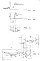
- FIG 3 illustrates a simplified write driver circuit.
- the write driver circuit includes an H-drive circuit 20 as described above, and a discharge circuit 22.
- the H-drive circuit 20 includes P-MOS transistors in place of the NPN transistors shown in Figure 1 .
- the discharge circuit 22 provides a discharge path from the base of H-bridge 20 NPN 24 to ground that limits the current overshoot and allows a faster settling time. This results in maximizing write frequency and minimizing write asymmetry.
- the discharge circuit 22 includes an NPN transistor 26 with the collector connected to the base of the H-bridge transistor 24 and the emitter connected to ground.
- the base of NPN transistor 26 may be controlled by N-MOS transistor 28.
- the N-MOS transistor 28 has a drain connected to the base of transistor 24 and source connected to the base of transistor 26.
- the gate of transistor 28 has an input signal X, which is a pulse that drives the discharge circuit. The operation of the circuit is described below with reference to Figures 4 (a-c).
- Figures 4 (a-c) show the voltage, current, and timing diagrams for the circuit described above and shown in Figure 3 .
- the current drive of transistor 24 represented in Figure 4b is controlled by its base voltage. Current and voltage ringing are due to the inductive load of head 10 during a current reversal through the head.
- Figures 4a and 4b show the base voltage and current for transistor 24 without discharge circuit 22 shown in the heavy lines. It is desirable to reduce the drive current overshoot and ringing without increasing the rise time. After reaching the appropriate drive current level, the present invention discharges a portion of the base voltage on transistor 24 which begins decreasing the drive current. The reduction in drive current has the effect of decreasing the ringing period and current overshoot.
- Circuit 22 of Figure 3 is an NPN transistor connected to discharge voltage from the base of transistor 24 when turned on by transistor 28.
- Figure 4c shows input X which turns NMOS transistor 28 on at a delay D1 after Y goes high. X turns on transistor 28 for a time D2.
- the discharge circuit quickly reduces the base voltage of transistor 24 after X goes high and consequently reduces the overshoot of the drive current as shown by the dashed line in Figure 4a and 4b .
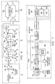
- the circuit includes the H-drive circuit 20 described above, and a modified version of discharge circuit 22.
- the discharge circuit 22 includes an NPN discharge transistor 26 collector connected to the base of the H-bridge transistor 24 and emitter connected to ground.
- the base of NPN transistor 26 is controlled by an N-MOS transistor pair 30, 32.
- the N-MOS transistor 30 has a drain connected to the base of transistor 24 and source connected to the base of transistor 26.
- the source of transistor 32 is connected to ground and drain connected to the base of transistor 26.
- the gates of transistors 30,32 are ultimately controlled by a pulse circuit 34 whose output is Nand gate 36.
- Transistor 30 is driven by the inverted output signal of Nand gate 36 through inverter 37.
- Pulse circuit 34 provides a pulse signal similar to input X of Figure 4c .
- the pulse signal is used to control the on time of discharge transistor 26 through transistors 30,32.
- Pulse circuit 34 of this embodiment comprises a three input Nand gate 36, an inverter 38 and delay elements 40,42.
- Nand gate 36 first input is the enabling input signal for the discharge circuit coming from the logic control circuit of the pre-amp (not shown).
- the second input is from the first delay element 40 which delays the input by a delay DLY1.
- the input to delay element 40 is Y , which is the same driver signal applied to the gate of the H-bridge transistor 24. Y and Y control the direction of write current through the write head.
- the third Nand input is driven by inverter 38.
- delay element 42 which provides a delay of DLY2 added to the delay of delay element 40(DLY1).
- Delay elements 40, 42 may include one or more active or passive devices and may be implemented in a number of ways as is commonly known in the art to achieve a signal delay.
- the operation of this circuit is as follows.
- the pre-amp control circuit first enables the discharge circuit by driving EN high. After a delay of DLY1 once Y goes high, the second input to Nand gate 36 goes high. Prior to the propagation of Y through delay circuit 42, inverter 38 has a high output to the third input to Nand gate 36. Therefor, output of Nand gate 36 switches low once the second input of Nand gate 36 goes high. This output is connected to inverter 37 which turns on transistor 30 which then turns on transistor 26. After a second delay corresponding to DLY2, the transition on Y will propagate through delay element 42 and inverter 38 to drive the third input to Nand gate 36 low and therefore switch the output of Nand gate 36 high and the output of inverter 37 low.
- the output of inverter 37 is a pulse similar to X shown in Figure 4c , it has a delay of DLY1 from Y and a period of DLY2.
- Transistor 30 is turned on during the pulse from inverter 37 while transistor 32 is turned off. Then during the pulse, transistor 26 in on and provides a discharge path from the base of transistor 24 to ground, as described above.
- Nand gate 36 has a high output which turns off transistor 30 and turns on transistor 32 to turn off the discharge path provided by transistor 26.
- FIG. 6 Another embodiment of the present invention is illustrated in Figure 6 .
- This embodiment also includes an H-bridge drive circuit 20 as described above, and a discharge circuit 22.
- the discharge circuit 22 includes a series of NPN discharge transistors 26 (a-c) with the collectors connected to the base of the H-bridge transistor 24 and the emitters connected to ground.
- the bases of the NPN transistors 26(a-c) are controlled by an N-MOS transistor pair 30, 32 through a select transistor 50, 52, 54.
- the N-MOS transistor pair 30, 32 are connected as in the previous embodiment described above.
- the base of transistors 30,32 are driven by the pulse circuit as described above.
- the select transistors 50, 52, 54 enable and disable the drive capability of the N-MOS transistor pair 30,32 to each discharge transistor 26(a-c).
- Select inputs Sell, Sel2 and Sel3 from the logic control circuit of the pre-amp connect to the gates of select transistors 50, 52, 54 to selectively enable one or more of the transistors.
- the size of transistors 26(a-c) can be scaled to provide a range of discharge current.
- the drain of a second transistor 56, 58, 60 is connected the base of each discharge transistor and the sources connected to ground.
- the gates of these transistors 56, 58, 60 are connected to the inverted select inputs from logic control to keep the transistors 26(a-c) off when they are not enabled.
- the embodiment of Figure 6 has the additional feature of a selectable discharge circuit.
- the control circuit of the write driver can selectively enable one or more of the transistors 26 (a-b) to provide a variable discharge current.
- a write driver circuit typically has a digital to analog converter (DAC) that controls the write current through the write head by controlling the signal value of Y and Y on the top or bottom devices of the H-bridge depending on which pair is used to control the steady state head current.
- the write driver circuit also will typically have a serial input to set the input to the DAC.
- the select inputs for the discharge circuit can be actuated by the control circuit according to the bits set in the write driver DAC, or the they could be actuated by an independent serial input register or other input external to the write driver. In this manner, the size of the discharge device can be controllably selected. The larger the size of the discharge device, the more discharge current is available. The selection may occur during design of the disk drive, during manufacture, or during operation of the disk drive.
- the duration of the discharge current can be controlled to optimize system performance.
- the duration of DLY1 and DLY2 could be optimized for a drive current range or be a fixed value, or the duration of DLY1 and DLY2 can be controlled to optimize the overshoot for a given disk drive design or to optimize a single unit at manufacture or during operation.
- Control of the duration could be as described above with control of the discharge current, that is it could be controlled using the write driver DAC or could be controlled independently.
- the period of DLY1 and DLY2 could be proportional to value of the steady state write head current controlled by the pre-amp DAC.
- the duration and the discharge current are both controlled to give a broad control of the overshoot.
- Figure 7 represents a HDD system level view of the present invention.
- the hard disk drive 100 is connected to a computer 102 through a controller 104.
- the hard disk drive 100 has disk platters 106, which are driven by motor 108 to rotate as shown.
- Read and write heads 110 move upon an actuator mechanism 112 driven by a voice coil motor 114.
- Data detected by the heads is passed through the pre-amp 116 and then a read channel 118 and also used to provide feedback to the head actuator position system 120.
- Data signals from the HDD are fed to the controller 102 which is then passed to the computer 104.
- the present invention concerns improvements to the head drive circuitry in the pre-amp 116 as discussed above.
- An advantage of the present invention is the manufacturer of the HDD can optimize the performance of the head by using the selectable nature of the current overshoot. Optimization could be done for a particular disk drive design, for a specific drive during burn-in, or "on the fly" when the head is accessing different tracks or sections of the disk platter.
Landscapes
- Digital Magnetic Recording (AREA)
Claims (5)
- Festplattenlaufwerk für ein Computersystem, Folgendes umfassend:eine oder mehrere Platten, die magnetische Medien auf einer oder mehreren Flächen aufweisen;einen Schreibkopf (10), der mit mindestens einer der Flächen, die magnetische Medien aufweisen, verknüpft ist;eine H-Brückenschaltung (20), die in der Lage ist, einen Strom durch den Schreibkopf (10) zu treiben, wobei die H-Brückenschaltung Folgendes umfasstzwei erste Transistoren (Y,
Y ) und zwei zweite Transistoren (Y , Y 24) undeine Entladungsschaltung (22), die mit mindestens einem der zwei Transistoren (24) verbunden und angeordnet ist, den Base/Gate-Antrieb des mindestens einen zweiten Transistors (24) erst zu entladen, nachdem der Strom durch den Kopf (10) über einen Beharrungswert ansteigt, wobei die Entladungsschaltung (22) mindestens einen Entladungstransistor (26, 28) umfasst, der mit einer Base bzw. einem Gate der zweiten Transistoren (24) an der H-Brücke verbunden ist, und gekennzeichnet durcheine Pulsschaltung (X, 34), die angeordnet ist, den Entladungstransistor (28, 26) nach einer ersten Verzögerung (D1, DLY1) ab dem Einschalten des zweiten Transistors (Y ) einzuschalten und den Entladungstransistor (28) nach einer zweiten Verzögerung (D2, DLY2) auszuschalten. - Festplattenlaufwerk nach Anspruch 1, wobei mindestens eine der ersten (D1, DLY1) und der zweiten (D2, DLY2) Verzögerungsperiode auswählbar gesteuert wird.
- Festplattenlaufwerk nach Anspruch 2, das ferner Folgendes umfasst:
einen Digital-Analog-Wandler (DAC) zum Steuern des Schreibstroms durch den Kopf (10), wobei sich mindestens eine der ersten (DLY1) und der zweiten (DLY2) Verzögerungsperiode proportional zum DAC-Schreibstrom verhält. - Festplattenlaufwerk nach einem der Ansprüche 1 bis 3, das ferner Folgendes umfasst:
eine Vielzahl von Entladungstransistoren (26a-c), die parallel mit den Gates der Vielzahl von Transistoren verbunden sind und einen ausgewählten Transistor (50, 52, 54) mit einem ausgewählten Eingang (Sel1, Sel2, Sel3) an einem Gateeingang aufweisen, wobei die Gateeingänge mit Mitteln zum Aktivieren von einem oder mehreren der ausgewählten Transistoren (50, 52, 54) verbunden sind. - Integrierte Schaltung zum Ansteuern des Schreibkopfes (10) des Festplattenlaufwerks nach einem der Ansprüche 1 bis 4.
Applications Claiming Priority (2)
| Application Number | Priority Date | Filing Date | Title |
|---|---|---|---|
| US474958 | 1983-03-14 | ||
| US09/474,958 US6549353B1 (en) | 1999-12-30 | 1999-12-30 | Overshoot control for a hard disk drive write head |
Publications (3)
| Publication Number | Publication Date |
|---|---|
| EP1113423A2 EP1113423A2 (de) | 2001-07-04 |
| EP1113423A3 EP1113423A3 (de) | 2006-07-05 |
| EP1113423B1 true EP1113423B1 (de) | 2019-09-04 |
Family
ID=23885673
Family Applications (1)
| Application Number | Title | Priority Date | Filing Date |
|---|---|---|---|
| EP00204583.9A Expired - Lifetime EP1113423B1 (de) | 1999-12-30 | 2000-12-18 | Verbesserungen bei Plattenlaufwerken |
Country Status (5)
| Country | Link |
|---|---|
| US (1) | US6549353B1 (de) |
| EP (1) | EP1113423B1 (de) |
| JP (1) | JP2001236603A (de) |
| KR (1) | KR100658014B1 (de) |
| TW (1) | TW594681B (de) |
Families Citing this family (14)
| Publication number | Priority date | Publication date | Assignee | Title |
|---|---|---|---|---|
| US20030111856A1 (en) * | 2001-12-13 | 2003-06-19 | Hewett Frank W. | Bundling, carrying and storing device |
| JP3648496B2 (ja) * | 2002-05-31 | 2005-05-18 | 株式会社東芝 | ディスク記憶装置及び同装置における記録電流制御方法 |
| US6879456B2 (en) * | 2002-08-15 | 2005-04-12 | Agere Systems Inc. | Disk drive writer with active reflection cancellation |
| KR100532479B1 (ko) * | 2002-11-14 | 2005-11-30 | 삼성전자주식회사 | 조립된 디스크 드라이브에서 최적화된 헤드 쓰기 컨트롤을위한 쓰기 전류의 오버슈트 컨트롤을 결정 및/또는사용하는 방법 및 장치 |
| US7151393B2 (en) * | 2004-11-05 | 2006-12-19 | Guzik Technical Enterprises | High-speed write driver |
| US20080002267A1 (en) * | 2006-06-29 | 2008-01-03 | Eun Kyu Jang | Method and apparatus for slew rate control in the write current shape of a hard disk drive |
| US20080204914A1 (en) * | 2007-02-27 | 2008-08-28 | Texas Instruments Incorporated | Low Power Write Driver for a Magnetic Disk Drive |
| US20080239558A1 (en) * | 2007-03-30 | 2008-10-02 | Jeremy Robert Kuehlwein | Methods and apparatus for duration control of hard drive write signals |
| US7855849B2 (en) * | 2007-03-30 | 2010-12-21 | Texas Instruments Incorporated | Methods and apparatus for temperature compensation for hard disk drive write overshoot current |
| US8040627B2 (en) * | 2007-03-30 | 2011-10-18 | Texas Instruments Incorporated | Methods and apparatus for generating a hard drive write signal |
| TWI358902B (en) * | 2007-12-31 | 2012-02-21 | Ind Tech Res Inst | Signal delay circuit |
| US8804261B2 (en) | 2012-07-27 | 2014-08-12 | Lsi Corporation | Over-the-rail write driver for magnetic storage systems |
| US9191013B1 (en) | 2013-10-24 | 2015-11-17 | Seagate Technology Llc | Voltage compensation |
| US11657846B1 (en) | 2022-03-31 | 2023-05-23 | Stmicroelectronics S.R.L. | Automatic skew calibration circuit for pattern-dependent dynamic wave shaping for HDD preamplifier write |
Citations (1)
| Publication number | Priority date | Publication date | Assignee | Title |
|---|---|---|---|---|
| JPS61137208A (ja) * | 1984-12-10 | 1986-06-24 | Nippon Telegr & Teleph Corp <Ntt> | デイジタル磁気記録電流波形等化方式 |
Family Cites Families (10)
| Publication number | Priority date | Publication date | Assignee | Title |
|---|---|---|---|---|
| JP3109889B2 (ja) * | 1992-01-30 | 2000-11-20 | 株式会社日立製作所 | 磁気ヘッド用回路 |
| US5287231A (en) * | 1992-10-06 | 1994-02-15 | Vtc Inc. | Write circuit having current mirrors between predriver and write driver circuits for maximum head voltage swing |
| US5296975A (en) * | 1992-10-09 | 1994-03-22 | International Business Machines Corporation | High-transition-rate, low-supply-voltage write driver circuitry for magnetic inductive write head |
| US5781046A (en) * | 1995-03-22 | 1998-07-14 | Vtc, Inc. | Push-and-pull driver circuit for driving an H-bridge coupled to a two-terminal inductive load |
| US5751171A (en) * | 1995-03-22 | 1998-05-12 | Vtc Inc. | Predriver for fast current switching through a two-terminal inductive load |
| KR0175279B1 (ko) * | 1996-04-04 | 1999-04-01 | 김광호 | Cmos 출력버퍼회로 |
| US5990710A (en) * | 1996-06-13 | 1999-11-23 | Vtc, Inc. | High performance write driver for magnetic inductive recording head |
| US6052017A (en) * | 1997-06-30 | 2000-04-18 | Stmicroelectronics, Inc. | Method and circuit for enabling rapid flux reversal in the coil of a write head associated with a computer disk drive, or the like |
| JPH11149604A (ja) * | 1997-09-12 | 1999-06-02 | St Microelectron Inc | コンピュータディスク駆動装置等に関連する書込ヘッドのコイル内の迅速な磁束反転を可能とする方法及び回路 |
| US6271978B1 (en) * | 1999-05-07 | 2001-08-07 | Texas Instruments Incorporated | Power efficient overshoot control for magnetic recording write driver |
-
1999
- 1999-12-30 US US09/474,958 patent/US6549353B1/en not_active Expired - Lifetime
-
2000
- 2000-12-18 EP EP00204583.9A patent/EP1113423B1/de not_active Expired - Lifetime
- 2000-12-28 JP JP2000402212A patent/JP2001236603A/ja active Pending
- 2000-12-29 KR KR1020000085210A patent/KR100658014B1/ko not_active Expired - Fee Related
-
2001
- 2001-02-07 TW TW089128068A patent/TW594681B/zh not_active IP Right Cessation
Patent Citations (1)
| Publication number | Priority date | Publication date | Assignee | Title |
|---|---|---|---|---|
| JPS61137208A (ja) * | 1984-12-10 | 1986-06-24 | Nippon Telegr & Teleph Corp <Ntt> | デイジタル磁気記録電流波形等化方式 |
Also Published As
| Publication number | Publication date |
|---|---|
| TW594681B (en) | 2004-06-21 |
| EP1113423A3 (de) | 2006-07-05 |
| KR100658014B1 (ko) | 2006-12-15 |
| EP1113423A2 (de) | 2001-07-04 |
| JP2001236603A (ja) | 2001-08-31 |
| US6549353B1 (en) | 2003-04-15 |
| KR20010062838A (ko) | 2001-07-07 |
Similar Documents
| Publication | Publication Date | Title |
|---|---|---|
| US5880626A (en) | Active damping for a disk drive write circuit | |
| EP1113423B1 (de) | Verbesserungen bei Plattenlaufwerken | |
| US6052017A (en) | Method and circuit for enabling rapid flux reversal in the coil of a write head associated with a computer disk drive, or the like | |
| US6496317B2 (en) | Accurate adjustable current overshoot circuit | |
| US6917484B2 (en) | Damping resistor boost writer architecture | |
| EP1014360B1 (de) | Verbesserungen bei Schreibköpfen für Festplattenlaufwerk | |
| EP1083549B1 (de) | Schaltung und Verfahren zum Schreiben auf einer Speicherplatte | |
| US6831800B2 (en) | Boost system and method to facilitate driving a load | |
| US6271978B1 (en) | Power efficient overshoot control for magnetic recording write driver | |
| EP1310955A2 (de) | Schreibkopf-treiberschaltung und Methode zum schreiben auf einer Speicherplatte | |
| KR20000011636A (ko) | 정보를자기저장매체에기록하는프로그램가능기록드라이버회로 | |
| US6512645B1 (en) | Circuit and method for writing to a memory disk with a boosted voltage | |
| US5910861A (en) | Technique for controlling the write currents of a magnetic disk recording apparatus | |
| US6259305B1 (en) | Method and apparatus to drive the coil of a magnetic write head | |
| US6198335B1 (en) | Method and apparatus to drive the coil of a magnetic write head | |
| US6128146A (en) | Undershoot active damping circuit for write drivers | |
| US6400190B1 (en) | Controlled current undershoot circuit | |
| US6731449B2 (en) | Magnetic recording writing circuit | |
| US6226141B1 (en) | Damp circuit for a hard disk drive write head | |
| US6580575B1 (en) | Process and temperature resistant active damping circuit for inductive write drivers | |
| US7453659B2 (en) | Circuit and method for write current driver | |
| US20250372120A1 (en) | High-speed high-voltage cmos write driver | |
| US20040042109A1 (en) | Power efficient overshoot protection during an operating mode transition | |
| US12573419B1 (en) | Selectable current booster circuit | |
| US20020101267A1 (en) | Ultra-fast voltage drive |
Legal Events
| Date | Code | Title | Description |
|---|---|---|---|
| PUAI | Public reference made under article 153(3) epc to a published international application that has entered the european phase |
Free format text: ORIGINAL CODE: 0009012 |
|
| AK | Designated contracting states |
Kind code of ref document: A2 Designated state(s): AT BE CH CY DE DK ES FI FR GB GR IE IT LI LU MC NL PT SE TR |
|
| AX | Request for extension of the european patent |
Free format text: AL;LT;LV;MK;RO;SI |
|
| 17P | Request for examination filed |
Effective date: 20010903 |
|
| PUAL | Search report despatched |
Free format text: ORIGINAL CODE: 0009013 |
|
| AK | Designated contracting states |
Kind code of ref document: A3 Designated state(s): AT BE CH CY DE DK ES FI FR GB GR IE IT LI LU MC NL PT SE TR |
|
| AX | Request for extension of the european patent |
Extension state: AL LT LV MK RO SI |
|
| AKX | Designation fees paid |
Designated state(s): AT BE CH CY DE DK ES FI FR GB GR IE IT LI LU MC NL PT SE TR |
|
| 17Q | First examination report despatched |
Effective date: 20070911 |
|
| STAA | Information on the status of an ep patent application or granted ep patent |
Free format text: STATUS: EXAMINATION IS IN PROGRESS |
|
| REG | Reference to a national code |
Ref country code: DE Ref legal event code: R079 Ref document number: 60049944 Country of ref document: DE Free format text: PREVIOUS MAIN CLASS: G11B0005012000 Ipc: G11B0019040000 |
|
| GRAP | Despatch of communication of intention to grant a patent |
Free format text: ORIGINAL CODE: EPIDOSNIGR1 |
|
| STAA | Information on the status of an ep patent application or granted ep patent |
Free format text: STATUS: GRANT OF PATENT IS INTENDED |
|
| RIC1 | Information provided on ipc code assigned before grant |
Ipc: G11B 5/02 20060101ALI20190304BHEP Ipc: G11B 5/012 20060101ALI20190304BHEP Ipc: G11B 5/09 20060101ALI20190304BHEP Ipc: G11B 19/04 20060101AFI20190304BHEP |
|
| INTG | Intention to grant announced |
Effective date: 20190328 |
|
| GRAS | Grant fee paid |
Free format text: ORIGINAL CODE: EPIDOSNIGR3 |
|
| GRAA | (expected) grant |
Free format text: ORIGINAL CODE: 0009210 |
|
| STAA | Information on the status of an ep patent application or granted ep patent |
Free format text: STATUS: THE PATENT HAS BEEN GRANTED |
|
| AK | Designated contracting states |
Kind code of ref document: B1 Designated state(s): AT BE CH CY DE DK ES FI FR GB GR IE IT LI LU MC NL PT SE TR |
|
| REG | Reference to a national code |
Ref country code: GB Ref legal event code: FG4D |
|
| REG | Reference to a national code |
Ref country code: CH Ref legal event code: EP |
|
| REG | Reference to a national code |
Ref country code: AT Ref legal event code: REF Ref document number: 1176499 Country of ref document: AT Kind code of ref document: T Effective date: 20190915 |
|
| REG | Reference to a national code |
Ref country code: DE Ref legal event code: R096 Ref document number: 60049944 Country of ref document: DE |
|
| REG | Reference to a national code |
Ref country code: IE Ref legal event code: FG4D |
|
| REG | Reference to a national code |
Ref country code: NL Ref legal event code: MP Effective date: 20190904 |
|
| PG25 | Lapsed in a contracting state [announced via postgrant information from national office to epo] |
Ref country code: FI Free format text: LAPSE BECAUSE OF FAILURE TO SUBMIT A TRANSLATION OF THE DESCRIPTION OR TO PAY THE FEE WITHIN THE PRESCRIBED TIME-LIMIT Effective date: 20190904 Ref country code: SE Free format text: LAPSE BECAUSE OF FAILURE TO SUBMIT A TRANSLATION OF THE DESCRIPTION OR TO PAY THE FEE WITHIN THE PRESCRIBED TIME-LIMIT Effective date: 20190904 |
|
| PG25 | Lapsed in a contracting state [announced via postgrant information from national office to epo] |
Ref country code: ES Free format text: LAPSE BECAUSE OF FAILURE TO SUBMIT A TRANSLATION OF THE DESCRIPTION OR TO PAY THE FEE WITHIN THE PRESCRIBED TIME-LIMIT Effective date: 20190904 Ref country code: GR Free format text: LAPSE BECAUSE OF FAILURE TO SUBMIT A TRANSLATION OF THE DESCRIPTION OR TO PAY THE FEE WITHIN THE PRESCRIBED TIME-LIMIT Effective date: 20191205 |
|
| REG | Reference to a national code |
Ref country code: AT Ref legal event code: MK05 Ref document number: 1176499 Country of ref document: AT Kind code of ref document: T Effective date: 20190904 |
|
| PG25 | Lapsed in a contracting state [announced via postgrant information from national office to epo] |
Ref country code: IT Free format text: LAPSE BECAUSE OF FAILURE TO SUBMIT A TRANSLATION OF THE DESCRIPTION OR TO PAY THE FEE WITHIN THE PRESCRIBED TIME-LIMIT Effective date: 20190904 Ref country code: PT Free format text: LAPSE BECAUSE OF FAILURE TO SUBMIT A TRANSLATION OF THE DESCRIPTION OR TO PAY THE FEE WITHIN THE PRESCRIBED TIME-LIMIT Effective date: 20200106 Ref country code: NL Free format text: LAPSE BECAUSE OF FAILURE TO SUBMIT A TRANSLATION OF THE DESCRIPTION OR TO PAY THE FEE WITHIN THE PRESCRIBED TIME-LIMIT Effective date: 20190904 Ref country code: AT Free format text: LAPSE BECAUSE OF FAILURE TO SUBMIT A TRANSLATION OF THE DESCRIPTION OR TO PAY THE FEE WITHIN THE PRESCRIBED TIME-LIMIT Effective date: 20190904 |
|
| REG | Reference to a national code |
Ref country code: DE Ref legal event code: R097 Ref document number: 60049944 Country of ref document: DE |
|
| REG | Reference to a national code |
Ref country code: DE Ref legal event code: R119 Ref document number: 60049944 Country of ref document: DE |
|
| PLBE | No opposition filed within time limit |
Free format text: ORIGINAL CODE: 0009261 |
|
| STAA | Information on the status of an ep patent application or granted ep patent |
Free format text: STATUS: NO OPPOSITION FILED WITHIN TIME LIMIT |
|
| PG25 | Lapsed in a contracting state [announced via postgrant information from national office to epo] |
Ref country code: DK Free format text: LAPSE BECAUSE OF FAILURE TO SUBMIT A TRANSLATION OF THE DESCRIPTION OR TO PAY THE FEE WITHIN THE PRESCRIBED TIME-LIMIT Effective date: 20190904 |
|
| REG | Reference to a national code |
Ref country code: CH Ref legal event code: PL |
|
| 26N | No opposition filed |
Effective date: 20200605 |
|
| REG | Reference to a national code |
Ref country code: BE Ref legal event code: MM Effective date: 20191231 |
|
| PG25 | Lapsed in a contracting state [announced via postgrant information from national office to epo] |
Ref country code: MC Free format text: LAPSE BECAUSE OF FAILURE TO SUBMIT A TRANSLATION OF THE DESCRIPTION OR TO PAY THE FEE WITHIN THE PRESCRIBED TIME-LIMIT Effective date: 20190904 |
|
| GBPC | Gb: european patent ceased through non-payment of renewal fee |
Effective date: 20191218 |
|
| PG25 | Lapsed in a contracting state [announced via postgrant information from national office to epo] |
Ref country code: LU Free format text: LAPSE BECAUSE OF NON-PAYMENT OF DUE FEES Effective date: 20191218 Ref country code: GB Free format text: LAPSE BECAUSE OF NON-PAYMENT OF DUE FEES Effective date: 20191218 Ref country code: DE Free format text: LAPSE BECAUSE OF NON-PAYMENT OF DUE FEES Effective date: 20200701 Ref country code: IE Free format text: LAPSE BECAUSE OF NON-PAYMENT OF DUE FEES Effective date: 20191218 Ref country code: FR Free format text: LAPSE BECAUSE OF NON-PAYMENT OF DUE FEES Effective date: 20191231 |
|
| PG25 | Lapsed in a contracting state [announced via postgrant information from national office to epo] |
Ref country code: LI Free format text: LAPSE BECAUSE OF NON-PAYMENT OF DUE FEES Effective date: 20191231 Ref country code: CH Free format text: LAPSE BECAUSE OF NON-PAYMENT OF DUE FEES Effective date: 20191231 Ref country code: BE Free format text: LAPSE BECAUSE OF NON-PAYMENT OF DUE FEES Effective date: 20191231 |
|
| PG25 | Lapsed in a contracting state [announced via postgrant information from national office to epo] |
Ref country code: CY Free format text: LAPSE BECAUSE OF FAILURE TO SUBMIT A TRANSLATION OF THE DESCRIPTION OR TO PAY THE FEE WITHIN THE PRESCRIBED TIME-LIMIT Effective date: 20190904 |
|
| PG25 | Lapsed in a contracting state [announced via postgrant information from national office to epo] |
Ref country code: TR Free format text: LAPSE BECAUSE OF FAILURE TO SUBMIT A TRANSLATION OF THE DESCRIPTION OR TO PAY THE FEE WITHIN THE PRESCRIBED TIME-LIMIT Effective date: 20190904 |