EP1113531A2 - Elektrischer Kontakt mit orthogonalen Kontaktarmen und versetzten Kontaktflächen und dessen Herstellungsverfahren - Google Patents
Elektrischer Kontakt mit orthogonalen Kontaktarmen und versetzten Kontaktflächen und dessen Herstellungsverfahren Download PDFInfo
- Publication number
- EP1113531A2 EP1113531A2 EP00128224A EP00128224A EP1113531A2 EP 1113531 A2 EP1113531 A2 EP 1113531A2 EP 00128224 A EP00128224 A EP 00128224A EP 00128224 A EP00128224 A EP 00128224A EP 1113531 A2 EP1113531 A2 EP 1113531A2
- Authority
- EP
- European Patent Office
- Prior art keywords
- contact
- arms
- male
- electrical
- area
- Prior art date
- Legal status (The legal status is an assumption and is not a legal conclusion. Google has not performed a legal analysis and makes no representation as to the accuracy of the status listed.)
- Withdrawn
Links
Images


Classifications
-
- H—ELECTRICITY
- H01—ELECTRIC ELEMENTS
- H01R—ELECTRICALLY-CONDUCTIVE CONNECTIONS; STRUCTURAL ASSOCIATIONS OF A PLURALITY OF MUTUALLY-INSULATED ELECTRICAL CONNECTING ELEMENTS; COUPLING DEVICES; CURRENT COLLECTORS
- H01R11/00—Individual connecting elements providing two or more spaced connecting locations for conductive members which are, or may be, thereby interconnected, e.g. end pieces for wires or cables supported by the wire or cable and having means for facilitating electrical connection to some other wire, terminal, or conductive member, blocks of binding posts
- H01R11/11—End pieces or tapping pieces for wires, supported by the wire and for facilitating electrical connection to some other wire, terminal or conductive member
- H01R11/22—End pieces terminating in a spring clip
-
- H—ELECTRICITY
- H01—ELECTRIC ELEMENTS
- H01R—ELECTRICALLY-CONDUCTIVE CONNECTIONS; STRUCTURAL ASSOCIATIONS OF A PLURALITY OF MUTUALLY-INSULATED ELECTRICAL CONNECTING ELEMENTS; COUPLING DEVICES; CURRENT COLLECTORS
- H01R13/00—Details of coupling devices of the kinds covered by groups H01R12/70 or H01R24/00 - H01R33/00
- H01R13/02—Contact members
- H01R13/10—Sockets for co-operation with pins or blades
- H01R13/11—Resilient sockets
- H01R13/113—Resilient sockets co-operating with pins or blades having a rectangular transverse section
-
- H—ELECTRICITY
- H01—ELECTRIC ELEMENTS
- H01R—ELECTRICALLY-CONDUCTIVE CONNECTIONS; STRUCTURAL ASSOCIATIONS OF A PLURALITY OF MUTUALLY-INSULATED ELECTRICAL CONNECTING ELEMENTS; COUPLING DEVICES; CURRENT COLLECTORS
- H01R13/00—Details of coupling devices of the kinds covered by groups H01R12/70 or H01R24/00 - H01R33/00
- H01R13/02—Contact members
- H01R13/10—Sockets for co-operation with pins or blades
- H01R13/11—Resilient sockets
- H01R13/112—Resilient sockets forked sockets having two legs
-
- H—ELECTRICITY
- H01—ELECTRIC ELEMENTS
- H01R—ELECTRICALLY-CONDUCTIVE CONNECTIONS; STRUCTURAL ASSOCIATIONS OF A PLURALITY OF MUTUALLY-INSULATED ELECTRICAL CONNECTING ELEMENTS; COUPLING DEVICES; CURRENT COLLECTORS
- H01R12/00—Structural associations of a plurality of mutually-insulated electrical connecting elements, specially adapted for printed circuits, e.g. printed circuit boards [PCB], flat or ribbon cables, or like generally planar structures, e.g. terminal strips, terminal blocks; Coupling devices specially adapted for printed circuits, flat or ribbon cables, or like generally planar structures; Terminals specially adapted for contact with, or insertion into, printed circuits, flat or ribbon cables, or like generally planar structures
- H01R12/50—Fixed connections
- H01R12/51—Fixed connections for rigid printed circuits or like structures
- H01R12/55—Fixed connections for rigid printed circuits or like structures characterised by the terminals
- H01R12/58—Fixed connections for rigid printed circuits or like structures characterised by the terminals terminals for insertion into holes
- H01R12/585—Terminals having a press fit or a compliant portion and a shank passing through a hole in the printed circuit board
-
- H—ELECTRICITY
- H01—ELECTRIC ELEMENTS
- H01R—ELECTRICALLY-CONDUCTIVE CONNECTIONS; STRUCTURAL ASSOCIATIONS OF A PLURALITY OF MUTUALLY-INSULATED ELECTRICAL CONNECTING ELEMENTS; COUPLING DEVICES; CURRENT COLLECTORS
- H01R13/00—Details of coupling devices of the kinds covered by groups H01R12/70 or H01R24/00 - H01R33/00
- H01R13/648—Protective earth or shield arrangements on coupling devices, e.g. anti-static shielding
- H01R13/658—High frequency shielding arrangements, e.g. against EMI [Electro-Magnetic Interference] or EMP [Electro-Magnetic Pulse]
- H01R13/6581—Shield structure
- H01R13/6585—Shielding material individually surrounding or interposed between mutually spaced contacts
- H01R13/6586—Shielding material individually surrounding or interposed between mutually spaced contacts for separating multiple connector modules
-
- H—ELECTRICITY
- H01—ELECTRIC ELEMENTS
- H01R—ELECTRICALLY-CONDUCTIVE CONNECTIONS; STRUCTURAL ASSOCIATIONS OF A PLURALITY OF MUTUALLY-INSULATED ELECTRICAL CONNECTING ELEMENTS; COUPLING DEVICES; CURRENT COLLECTORS
- H01R13/00—Details of coupling devices of the kinds covered by groups H01R12/70 or H01R24/00 - H01R33/00
- H01R13/648—Protective earth or shield arrangements on coupling devices, e.g. anti-static shielding
- H01R13/658—High frequency shielding arrangements, e.g. against EMI [Electro-Magnetic Interference] or EMP [Electro-Magnetic Pulse]
- H01R13/6581—Shield structure
- H01R13/6585—Shielding material individually surrounding or interposed between mutually spaced contacts
- H01R13/6586—Shielding material individually surrounding or interposed between mutually spaced contacts for separating multiple connector modules
- H01R13/6587—Shielding material individually surrounding or interposed between mutually spaced contacts for separating multiple connector modules for mounting on PCBs
Definitions
- the present invention relates to electrical contacts and, more particularly, to an electrical contact with orthogonal contact arms and offset contact areas.
- U.S. Patent 5,711,690 discloses a card edge connector having an electrical contact with two orthogonally bent contact arms and offset contact areas between the two arms.
- U.S. Patent 4,607,907 discloses an electrical contact with generally parallel, but offset contact portions which overlap in a path of insertion of a male pin between the two contact areas.
- a problem with conventional electrical contacts which are intended to receive a mating male contact is that contact arm deflection can vary too much to be efficiently used in electrical connectors with very small spacings or pitch between contacts.
- an electrical contact comprising a first contact arm having a first contact area; and a second contact arm having a second contact area.
- the first and second contact arms form a male contact receiving area therebetween.
- the first and second contact arms are generally orthogonal to each other with a relatively narrow side edge of the first contact arm forming the first contact area and facing a relatively wide side face of the second contact arm which forms the second contact area.
- an electrical contact comprising a first connection section for connection to a first electrical component; and a second connection section, connected to the first connection section, for connection to a second electrical component.
- the second connection section comprises two contact arms forming a male contact receiving area therebetween.
- the two contact arms each have a male contact contacting area which are longitudinally offset from each other along a path of insertion of the male contact into the contact receiving area. Before the male contact is inserted into the contact receiving area, the two contacting areas overlap each other through the path of insertion of the male contact.
- a method of manufacturing an electrical contact comprising steps of providing a one-piece member with a first section having two contact arms; forming a first contact area on a first relatively narrow face of a first one of the contact arms, and a second contact area on a second relatively wide face of a second one of the contact arms; and bending the one-piece member to locate the two contact arms into a general orthogonal position relative to each other such that the first and second faces are located opposite each other and form a male contact receiving area therebetween.
- FIG. 1 there is shown a perspective view of an electrical contact 10 incorporating features of the present invention.
- an electrical contact 10 incorporating features of the present invention.
- the present invention will be described with reference to the single embodiment shown in the drawings, it should be understood that the present invention can be embodied in many alternate forms of embodiments.
- any suitable size, shape or type of elements or materials could be used.
- the contact 10 generally comprises a first connection or mounting section 12, a second connection or mating section 14, and a middle section 16 therebetween.
- the contact 10 is a one-piece member preferably stamped and formed from a flat conductive member, such as from a sheet of copper alloy.
- the contact could be comprised of more than one member and/or could be formed in any suitable manner and/or from any suitable stock material.
- the first connection section 12 is a press-fit through-hole solder tail.
- any suitable first connection section could be provided, such as a surface mount solder tail.
- the middle section 16 can have any suitable length and shape.
- the middle section 16 has a series of angled sections to form a right turn shape for use in a right angle connector, but the middle section could have a straight shape for a vertical or straight connector.
- the middle section 16 has a bent section 17 to locate the middle section 16 a selected distance from other middle sections 16 of adjacent contacts 10 in a connector.
- the first connection section 12 and the middle section 16 could have any suitable shape.
- the second connection section 14 generally comprises two contact arms 18,20 connected to each other by a base 22.
- the second connection section could have more than two contact arms.
- the base 22 need not be provided, such as when the contact arms project directly off of the middle section 16.
- the base 22 has a general cross-sectional "L" shape with two sections 24,26 connected to each other at a 90° bend or corner 28.
- the first section 24 preferably extends directly from and parallel with the middle section 16.
- the second section 26 and/or the corner 28 could extend directly from the middle section.
- the bend 28 could also be more or less than 90°. Referring also to Figs.
- the two contact arms 18,20 extend from the base 22 in a general cantilever fashion.
- the first contact arm 18 generally comprises, in series, a section 30 extending from the first section 24 of the base 22, a bend 32, and a front contact section 34.
- the second contact arm 20 generally comprises, in series, a section 36 extending from the second section 26 of the base 22, a bend 38, a section 40, and a front contact section 42.
- the bend 32 in the first arm 18 locates the front contact section 34 of the first contact arm 18 directly under the section 40 and front contact section 42 of the second contact arm 20.
- the first arm's front contact section 34 generally comprises a top side 44 having a protrusion 46 and a lead-in surface 48.
- the sloped surface leads to a male contact contacting area 50 on the protrusion 46.
- the first arm's front contact section 34 can have a relatively narrow width W 1 , and a relatively tall height H 1 .
- the bend 38 in the second contact arm 20 angles the section 40 toward the protrusion 46.
- the second arm's front contact section 42 generally comprises a formed curved shape with bottom surface 52 having a male contact contacting area 54.
- the curvature at the front end 53 of the bottom surface 52 forms a cam surface to interact with a mating male contact.
- the two contacting areas 50,54 are offset from each other by a length L relative to the insertion path of the male contact through the front end of the contact 10.
- the bend 38 in the second contact arm 20 preferably results in the second contact arm 20 being biased or preloaded against the first contact arm 18. However, in an alternate embodiment a preload need not be provided.
- the bottom surface 52 of the second contact arm 20 contacts the top surface 44 of the first contact arm 18 on the sloped surface 48.
- any suitable contact points could be provided.
- the arms 18, 20 need not contact each other in the home state.
- the two contact arms 18,20 are shown with a mating male contact P, such as a pin.
- the pin P can be inserted between the two arms 18,20 in a longitudinal path or direction of insertion I.
- the pin P has a height or width D 2 .
- the curvature of the second contact arm's front contact area 42, and the protrusion 46 and sloped surface 48 on the first contact arm 18 provide an overlap distance D 1 wherein the contacting area 54 is located below the contacting area 50.
- the two contacting areas overlap each other through the intended path I of insertion of the male contact P between the two contact arms.
- the arms 18,20 When the male contact P is inserted between the two arms 18,20, the arms 18,20 must be moved relative to each other a combined distance of D 1 and D 2 .
- the present invention provides an increased beam or arm deflection; more than a deflection merely equal to the male contact's width D 2 .
- arms 18, 20 engage opposing sides of male contact P.
- the orthogonal arrangement of the arms 18,20 also provides for a more predictable arm or beam deflection when the male contact P is inserted.
- the height H 1 of the first contact arm 18 is relatively larger than the height H 2 of the second contact arm 20. Therefore, the second arm 20 will deflect more than the first arm 18 when the male contact P is inserted.
- the height H 1 of the first arm 18 can be easily selected when the first arm 18 is initially stamped and formed to provide any suitable deflection differential between the two arms 18,20.
- the first arm 18 could be sized and shaped to have almost no deflection when the male contact P is inserted.
- H 1 could be less than H 2 , or H 1 could be equal to H 2 .
- W 1 and H 2 are preferably constant based upon the thickness of the stock material.
- positioning of the male contact P between the two arms 18,20 can be more precisely controlled which can be beneficial in electrical connectors with a relatively small contact pitch, such as 1 mm or less.
- the present invention also provides another advantage.
- the area 50 can be cross-sectionally flat.
- the area 50 could be coined if an even higher contact force is desired.
- the area 54 could also be coined to form a contact curvature if desired.
- edge 44 is a cut or stamped edge.
- the two arms 18,20 form a general cross-sectional "T" shaped interface.
- the bottom beam is an "edge of stock" feature while the top beam is a formed feature.
- the overlapping geometry proves redundant contact points.
- the combination of D 1 and D 2 illustrates the increased deflection created by the contact beam geometry. This deflection range and corresponding mating force can be modified to meet the specific needs of different applications by modifying the beam/arm geometry.
- the contact arms 18, 20 could be sized and shaped such that forces against the arms, exerted by an inserted male contact, cancel each other out. Therefore, total forces on a connector housing in which the contact is mounted are counteracted. If the forces on individual contacts do not cancel each other out, each contact could be arranged relative to another contact such that the "T" shaped interfaces are in opposite positions. Thus, the combined forces could counteract each other.
- the receptacle 100 generally comprises a housing 102 and a module assembly 104 connected to the housing 102.
- the housing 102 generally comprises a first housing member 106 and a second housing member 108.
- the first and second housing members 106, 108 are preferably comprised of a dielectric material, such as a molded plastic or polymer material.
- the first housing member 106 includes a top 110, a back 112, two sides 114, a generally open front, a generally open bottom, and a receiving area 120.
- the top 110 includes module mounting holes 122.
- the back 112 includes module mounting holes 124.
- the front includes extensions from the sides 114 for insertion into and connection with the second housing member 108.
- the second housing member 108 includes apertures or lead-ins through a front face 130 for insertion of front ends of a mating connector's male pins into the connector 100.
- the module assembly 104 generally comprises six contact modules 132 (one of which is shown in Fig. 8A) and may include an additional ground member (not shown). In alternate embodiments more or less than six contact modules could be provided and, more or less than one ground member could be provided.
- the contact modules 132 comprise two sets of two types of contact modules which are preferably mirror images of each other. The ground member is sandwiched between the two sets.
- Each contact module 132 generally comprises a frame 140, signal contacts 142, and ground contacts 144.
- the frame 140 is preferably comprised of dielectric material, such as molded plastic or polymer.
- the frame 140 comprises a top side 146, a bottom side 148, a rear side 150, a front side 152, and two lateral sides 154, 156.
- the top side 146 includes a latch 158.
- the latch 158 is inserted into one of the module mounting holes 122 to connect the contact module 132 to the first housing member 106.
- the rear side 150 also includes a projection 160.
- the projection 160 is inserted into one of the module mounting holes 124 to connect the module 132 to the first housing member 106.
- the frame 140 includes channels 162 along at least one of the sides 154 for receiving portions of the ground contacts 144.
- the frame 140 could also have channels for receiving portions of the signal contacts 142.
- the frame 140 is preferably over-molded onto portions of the signal contacts 142.
- the frame 140 could be over-molded onto portions of the ground contacts 144.
- the front side 152 of the frame 140 includes pockets 164 and receiving area 165.
- each contact module has six of the signal contacts 142; three as a first type 142a of signal contacts and three as a second type 142b of signal contacts.
- the signal contacts 142 each have a first end 166, a middle section 168, and a second end 170.
- the first ends 166 have through-hole solder tails, but any suitable first ends could be provided, such as surface mount solder tails.
- the middle sections 168 all have right turn shapes, but with different lengths or dimensions to allow the signal contacts to be aligned in a row or common plane.
- the second ends 170 each comprise two deflectable arms 172, 174 oriented 90° offset from each other.
- the arms 172, 174 in the first type of signal contact 142a are orientated as mirror images of the arms 172, 174 in the second type of signal contacts 142b.
- the signal contacts 142 generally incorporate features of the contact 10. More specifically, the second ends 170 are structured similar to the second connection section 14 with the arms 172, 174 corresponding to the arms 18, 20.
- the signal contacts 142 can have the bend 28 in the upper left hand corner, the upper right hand corner, the lower left hand corner or the lower right hand corner of the second ends 170.
- the arms 172 (equivalent to arm 20) are located on only the top or bottom of the second ends 170 (as illustrated in Fig. 8C) and the arms 174 (equivalent to arm 18) extend from either the right side or the left side depending upon which one of the six contact modules 132 they are in. In alternate embodiments other types or orientations of the second ends could be provided.
- the ground contacts 144 for each module 132 can be provided as a single one-piece member or multiple members as shown.
- Each ground contact 144 includes a first end 176, a middle section 178, and a second end 180.
- the first ends 176 have through-hole solder tails. However, any suitable types of first ends could be provided, such as surface mount solder tails.
- the middle sections 178 generally comprise first sections 182 and second sections 184.
- the first sections 182 are located in the slots 162 of the frame 104 to fixedly connect the ground contacts 144 to the frame 140.
- the second sections 184 extend along the side surfaces 154 of the frame 140.
- the middle sections '178 have a general right turn shape such that the two ends 176, 180 are at a general right angle to each other.
- the second ends 180 include three different types of second ends.
- the first type of second end has a slot at a corner with a top arm and a side arm on opposite sides of the slot.
- the deflectable projections extend from the arms.
- the second type of second end is generally a mirror image of the first type of second end.
- the third type of end has two slots at two corners with a top arm, a bottom arm and a side arm. Two deflectable projections extend into the first slot, and two deflectable projections extend into the second slot.
- the side arm also includes a third slot.
- any suitable type(s) of second ends could be provided.
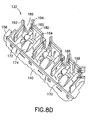
- a partial enlarged view of the front end of one of the modules 132 is shown.
- the two arms 172, 174 of each second end 170 of the signal contacts 142 are located in front of one of the pockets 164.
- a signal pin from a mating connector when inserted through one of the lead-ins of the housing, extends between the two arms 172, 174 into the pocket 164.
- the arms 172, 174 resiliently deflect outward.
- the slots 186 of the ground contacts 144 are located at the receiving areas 165 of the modules' frame 140.
- a ground pin from the mating connector can extend into the slot 186 and receiving area 165 between the two projections 192, 194.
- the ground member 134 also has a front end for connection to ground pins from the mating connector.
Landscapes
- Coupling Device And Connection With Printed Circuit (AREA)
- Details Of Connecting Devices For Male And Female Coupling (AREA)
- Manufacture Of Switches (AREA)
- Multi-Conductor Connections (AREA)
- Connector Housings Or Holding Contact Members (AREA)
Priority Applications (1)
| Application Number | Priority Date | Filing Date | Title |
|---|---|---|---|
| EP03024505A EP1398852B1 (de) | 1999-12-29 | 2000-12-22 | Elektrischer Kontakt mit orthogonalen Kontaktarmen und versetzten Kontaktflächen und dessen Herstellungsverfahren |
Applications Claiming Priority (2)
| Application Number | Priority Date | Filing Date | Title |
|---|---|---|---|
| US473771 | 1995-06-06 | ||
| US09/473,771 US6224432B1 (en) | 1999-12-29 | 1999-12-29 | Electrical contact with orthogonal contact arms and offset contact areas |
Related Child Applications (1)
| Application Number | Title | Priority Date | Filing Date |
|---|---|---|---|
| EP03024505A Division EP1398852B1 (de) | 1999-12-29 | 2000-12-22 | Elektrischer Kontakt mit orthogonalen Kontaktarmen und versetzten Kontaktflächen und dessen Herstellungsverfahren |
Publications (2)
| Publication Number | Publication Date |
|---|---|
| EP1113531A2 true EP1113531A2 (de) | 2001-07-04 |
| EP1113531A3 EP1113531A3 (de) | 2002-04-17 |
Family
ID=23880918
Family Applications (2)
| Application Number | Title | Priority Date | Filing Date |
|---|---|---|---|
| EP03024505A Expired - Lifetime EP1398852B1 (de) | 1999-12-29 | 2000-12-22 | Elektrischer Kontakt mit orthogonalen Kontaktarmen und versetzten Kontaktflächen und dessen Herstellungsverfahren |
| EP00128224A Withdrawn EP1113531A3 (de) | 1999-12-29 | 2000-12-22 | Elektrischer Kontakt mit orthogonalen Kontaktarmen und versetzten Kontaktflächen und dessen Herstellungsverfahren |
Family Applications Before (1)
| Application Number | Title | Priority Date | Filing Date |
|---|---|---|---|
| EP03024505A Expired - Lifetime EP1398852B1 (de) | 1999-12-29 | 2000-12-22 | Elektrischer Kontakt mit orthogonalen Kontaktarmen und versetzten Kontaktflächen und dessen Herstellungsverfahren |
Country Status (7)
| Country | Link |
|---|---|
| US (1) | US6224432B1 (de) |
| EP (2) | EP1398852B1 (de) |
| JP (1) | JP2001203027A (de) |
| KR (1) | KR100666067B1 (de) |
| AT (1) | ATE320092T1 (de) |
| CA (1) | CA2329669A1 (de) |
| DE (1) | DE60026625T2 (de) |
Cited By (1)
| Publication number | Priority date | Publication date | Assignee | Title |
|---|---|---|---|---|
| CN105359343A (zh) * | 2013-06-26 | 2016-02-24 | 矢崎总业株式会社 | 端子接头及其制造方法,以及使用该端子接头的连接器 |
Families Citing this family (38)
| Publication number | Priority date | Publication date | Assignee | Title |
|---|---|---|---|---|
| DE4330390C2 (de) * | 1993-09-08 | 1995-10-26 | Erni Elektroapp | Einteilige, zweischenklige Kontaktfeder |
| JP2001102118A (ja) * | 1999-10-01 | 2001-04-13 | Sumitomo Wiring Syst Ltd | フラットケーブル用コネクタ、フラットケーブル用コネクタに用いられる端子金具及びフラットケーブル用コネクタに用いられる端子金具の製造方法 |
| DE10027125A1 (de) * | 2000-05-31 | 2001-12-06 | Wabco Gmbh & Co Ohg | Elektrischer Steckkontakt |
| US6899566B2 (en) | 2002-01-28 | 2005-05-31 | Erni Elektroapparate Gmbh | Connector assembly interface for L-shaped ground shields and differential contact pairs |
| DE10331229A1 (de) * | 2003-07-10 | 2005-01-27 | Robert Bosch Gmbh | Kontaktanordnung bei einer elektrischen Steckverbindung |
| DE102005043692A1 (de) * | 2005-09-14 | 2007-03-15 | Robert Bosch Gmbh | Elektrischer Steckverbinder mit vorgespannten Kontaktlamellen |
| US7331802B2 (en) | 2005-11-02 | 2008-02-19 | Tyco Electronics Corporation | Orthogonal connector |
| WO2008156856A2 (en) * | 2007-06-20 | 2008-12-24 | Molex Incorporated | Connector with bifurcated contact arms |
| US7811100B2 (en) * | 2007-07-13 | 2010-10-12 | Fci Americas Technology, Inc. | Electrical connector system having a continuous ground at the mating interface thereof |
| US8764464B2 (en) | 2008-02-29 | 2014-07-01 | Fci Americas Technology Llc | Cross talk reduction for high speed electrical connectors |
| US7758385B2 (en) | 2008-03-07 | 2010-07-20 | Tyco Electronics Corporation | Orthogonal electrical connector and assembly |
| US8016616B2 (en) * | 2008-12-05 | 2011-09-13 | Tyco Electronics Corporation | Electrical connector system |
| US7775802B2 (en) * | 2008-12-05 | 2010-08-17 | Tyco Electronics Corporation | Electrical connector system |
| US7988456B2 (en) | 2009-01-14 | 2011-08-02 | Tyco Electronics Corporation | Orthogonal connector system |
| US7883366B2 (en) | 2009-02-02 | 2011-02-08 | Tyco Electronics Corporation | High density connector assembly |
| US9277649B2 (en) | 2009-02-26 | 2016-03-01 | Fci Americas Technology Llc | Cross talk reduction for high-speed electrical connectors |
| US8079847B2 (en) | 2009-06-01 | 2011-12-20 | Tyco Electronics Corporation | Orthogonal connector system with power connection |
| US7771244B1 (en) * | 2009-06-08 | 2010-08-10 | Lotes Co., Ltd | Electrical connector |
| US8267721B2 (en) | 2009-10-28 | 2012-09-18 | Fci Americas Technology Llc | Electrical connector having ground plates and ground coupling bar |
| US8616919B2 (en) | 2009-11-13 | 2013-12-31 | Fci Americas Technology Llc | Attachment system for electrical connector |
| TWI580122B (zh) * | 2010-02-26 | 2017-04-21 | 太谷電子公司 | 電氣連接器系統 |
| DE102012004833A1 (de) * | 2012-03-13 | 2013-09-19 | Lumberg Connect Gmbh | Steckkontakt zur Anordnung an einem Kontaktträger |
| JP5700026B2 (ja) * | 2012-11-28 | 2015-04-15 | 株式会社デンソー | 電装品機器の端子装置 |
| US9246293B2 (en) | 2013-10-31 | 2016-01-26 | Tyco Electronics Corporation | Leadframe for a contact module and method of manufacturing the same |
| DE102016108069A1 (de) * | 2016-05-02 | 2017-11-02 | Valeo Systèmes d'Essuyage | Kontaktelement zur Ausbildung einer elektrischen Verbindung mit einem Gegenelement, elektrische Verbindung und Scheibenwischermotor |
| CN105958245B (zh) * | 2016-06-08 | 2018-10-12 | 欧品电子(昆山)有限公司 | 高速连接器组件、插座连接器及其插座端子 |
| CN105914503B (zh) * | 2016-06-13 | 2018-10-12 | 欧品电子(昆山)有限公司 | 高速连接器组件、插座连接器及插头连接器 |
| CN106410473A (zh) * | 2016-06-22 | 2017-02-15 | 欧品电子(昆山)有限公司 | 高速连接器组件、插座连接器及其插座端子 |
| JP6765243B2 (ja) * | 2016-07-14 | 2020-10-07 | ヒロセ電機株式会社 | 電気コネクタ |
| CN106058544B (zh) * | 2016-08-03 | 2018-11-30 | 欧品电子(昆山)有限公司 | 高速连接器组件、插座连接器及插头连接器 |
| US10826205B2 (en) * | 2018-04-12 | 2020-11-03 | Panduit Corp. | Double wiping blade contact |
| TWD199072S (zh) * | 2018-07-05 | 2019-08-11 | Oupiin Electronic Kunshan Co Ltd | 具有兩個不等長不共面的分支的差分訊號端子 |
| CN108963510A (zh) * | 2018-07-05 | 2018-12-07 | 欧品电子(昆山)有限公司 | 高速连接器组件、插座连接器及其插座端子 |
| TWD199071S (zh) * | 2018-07-05 | 2019-08-11 | Oupiin Electronic Kunshan Co Ltd | 具有一卡口的差分訊號端子 |
| US10601195B2 (en) * | 2018-07-30 | 2020-03-24 | Lotes Co., Ltd | Electrical connector and electrical connector assembly capable of ensuring terminal positioning effect |
| CN109119793A (zh) * | 2018-08-17 | 2019-01-01 | 安费诺(常州)高端连接器有限公司 | 低串扰双接触高速背板连接器 |
| US20220294141A1 (en) * | 2021-03-11 | 2022-09-15 | Oupiin Electronic (Kunshan) Co., Ltd. | High-speed signal terminal, differential signal terminal pair and high-speed connector assembly |
| CN112886300B (zh) * | 2021-03-11 | 2024-09-10 | 欧品电子(昆山)有限公司 | 高速信号端子、差分信号端子对及高速连接器组合 |
Family Cites Families (34)
| Publication number | Priority date | Publication date | Assignee | Title |
|---|---|---|---|---|
| US3514740A (en) * | 1968-03-04 | 1970-05-26 | John Richard Filson | Wire-end connector structure |
| US3555493A (en) | 1968-03-25 | 1971-01-12 | Molex Products Co | Right angle printed circuit board connector |
| GB1226935A (de) * | 1968-09-23 | 1971-03-31 | ||
| US3862792A (en) * | 1973-10-03 | 1975-01-28 | Gte Sylvania Inc | Electrical connector assembly |
| USRE30277E (en) * | 1974-05-03 | 1980-05-20 | Amp Incorporated | Electrical tab receptacle |
| DE2515813A1 (de) | 1975-04-11 | 1976-10-21 | Bunker Ramo | Verfahren zum automatischen montieren und bestuecken von steckverbindern und nach dem verfahren hergestellte steckverbinder |
| US4004845A (en) * | 1975-04-17 | 1977-01-25 | Elco Corporation | High density electrical connector employing male blade with offset portions |
| US4175821A (en) | 1978-05-15 | 1979-11-27 | Teradyne, Inc. | Electrical connector |
| DE3028809C2 (de) * | 1980-07-30 | 1982-10-21 | Hermann Stribel KG, 7443 Frickenhausen | Steckeranordnung zur Aufnahme eines Flachsteckers |
| US4379611A (en) | 1980-11-03 | 1983-04-12 | Hughes Aircraft Company | Connector with low force socket contact having an integral hood |
| US4557548A (en) | 1983-12-14 | 1985-12-10 | Amp Incorporated | Edge connector for chip carrier |
| US4591230A (en) * | 1984-06-29 | 1986-05-27 | Frank Roldan | Electrical connector receptacle |
| US4607907A (en) | 1984-08-24 | 1986-08-26 | Burndy Corporation | Electrical connector requiring low mating force |
| US4776651A (en) * | 1985-12-06 | 1988-10-11 | Amp Incorporated | Socket contacts |
| US4973273A (en) | 1989-09-22 | 1990-11-27 | Robinson Nugent, Inc. | Dual-beam receptacle socket contact |
| JPH0731510Y2 (ja) * | 1990-05-16 | 1995-07-19 | 矢崎総業株式会社 | 雌端子金具 |
| JPH0748385B2 (ja) | 1990-07-13 | 1995-05-24 | 山一電機工業株式会社 | 三方向挟接形コンタクト |
| US5082459A (en) | 1990-08-23 | 1992-01-21 | Amp Incorporated | Dual readout simm socket |
| AU6402290A (en) | 1990-09-12 | 1992-03-30 | Thomas & Betts, France | Female connector with double-strip contacts |
| US5030107A (en) * | 1990-11-08 | 1991-07-09 | Molex Incorporated | LCD cluster connector |
| US5060372A (en) * | 1990-11-20 | 1991-10-29 | Capp Randolph E | Connector assembly and contacts with severed webs |
| JPH0636261U (ja) * | 1992-10-12 | 1994-05-13 | ホシデン株式会社 | メモリカード側多極コネクタ |
| JP2672450B2 (ja) | 1993-06-30 | 1997-11-05 | 山一電機株式会社 | 電気接触子 |
| US5435757A (en) * | 1993-07-27 | 1995-07-25 | The Whitaker Corporation | Contact and alignment feature |
| DE4400702C2 (de) * | 1994-01-12 | 2000-08-10 | Grote & Hartmann | Einstückige Steckervorrichtung |
| US5480316A (en) | 1994-06-23 | 1996-01-02 | The Whitaker Corporation | Low insertion force card edge connector |
| JP3067545B2 (ja) * | 1994-09-09 | 2000-07-17 | 住友電装株式会社 | 雌端子金具 |
| US5672084A (en) | 1995-03-29 | 1997-09-30 | Elco Corporation | High density connector receptacle |
| DE19541953A1 (de) | 1995-11-10 | 1997-05-15 | Harting Elektronik Gmbh | Kontaktfeder |
| US5676570A (en) | 1996-03-15 | 1997-10-14 | Minnesota Mining And Manufacturing Company | "F" port interface connector |
| JP3099111B2 (ja) * | 1996-05-31 | 2000-10-16 | モレックス インコーポレーテッド | リセプタクルコンタクトおよびリセプタクルコンタクトストリップ並びにリセプタクルコンタクトの製造方法 |
| US5711690A (en) | 1996-10-18 | 1998-01-27 | The Whitaker Corporation | Electrical contact and method for making same |
| US6227882B1 (en) * | 1997-10-01 | 2001-05-08 | Berg Technology, Inc. | Connector for electrical isolation in a condensed area |
| DE69929613T2 (de) | 1998-08-12 | 2006-09-28 | Robinson Nugent, Inc., New Albany | Verbindungsvorrichtung |
-
1999
- 1999-12-29 US US09/473,771 patent/US6224432B1/en not_active Expired - Lifetime
-
2000
- 2000-12-21 JP JP2000389363A patent/JP2001203027A/ja active Pending
- 2000-12-22 EP EP03024505A patent/EP1398852B1/de not_active Expired - Lifetime
- 2000-12-22 EP EP00128224A patent/EP1113531A3/de not_active Withdrawn
- 2000-12-22 DE DE60026625T patent/DE60026625T2/de not_active Expired - Lifetime
- 2000-12-22 AT AT03024505T patent/ATE320092T1/de not_active IP Right Cessation
- 2000-12-27 CA CA002329669A patent/CA2329669A1/en not_active Abandoned
- 2000-12-28 KR KR1020000083678A patent/KR100666067B1/ko not_active Expired - Fee Related
Cited By (1)
| Publication number | Priority date | Publication date | Assignee | Title |
|---|---|---|---|---|
| CN105359343A (zh) * | 2013-06-26 | 2016-02-24 | 矢崎总业株式会社 | 端子接头及其制造方法,以及使用该端子接头的连接器 |
Also Published As
| Publication number | Publication date |
|---|---|
| JP2001203027A (ja) | 2001-07-27 |
| DE60026625T2 (de) | 2006-09-21 |
| EP1398852B1 (de) | 2006-03-08 |
| ATE320092T1 (de) | 2006-03-15 |
| CA2329669A1 (en) | 2001-06-29 |
| EP1113531A3 (de) | 2002-04-17 |
| EP1398852A1 (de) | 2004-03-17 |
| KR100666067B1 (ko) | 2007-01-10 |
| KR20010062809A (en) | 2001-07-07 |
| US6224432B1 (en) | 2001-05-01 |
| DE60026625D1 (de) | 2006-05-04 |
Similar Documents
| Publication | Publication Date | Title |
|---|---|---|
| US6224432B1 (en) | Electrical contact with orthogonal contact arms and offset contact areas | |
| US5582519A (en) | Make-first-break-last ground connections | |
| US10566735B2 (en) | Connector | |
| US9680254B1 (en) | Connector and connector assembly | |
| JP4589362B2 (ja) | 高速、高密度電気コネクタ | |
| US8057263B1 (en) | Edge connectors having stamped signal contacts | |
| EP0724313A2 (de) | Auf eine Leiterplatte montierter elektrischer Steckverbinder | |
| EP0717468B1 (de) | Zuerst Polkontakte zuletzt Erdkontakt unterbrechender Steckverbinder | |
| CN110277678B (zh) | 连接器 | |
| US6062871A (en) | Interconnecting electrical connector | |
| EP0657959B1 (de) | Elektrische Verbinderanordnung zum Montieren auf gedruckte Leiterplatten | |
| JP2019071184A (ja) | コネクタ | |
| US10530081B1 (en) | Dual connector assembly for a circuit board | |
| EP0365179A1 (de) | Elektrisches Verbindersystem | |
| EP0542068B1 (de) | Elektrische Kontaktbuchse | |
| US6634899B2 (en) | Card edge connector | |
| US5938456A (en) | Low profile electrical connector | |
| JPH11502053A (ja) | 電気リセプタクル組立体及びそのためのばねコンタクト | |
| US7892033B2 (en) | Electrical connector ensuring proper connection | |
| US20060135003A1 (en) | Connector with improved dual beam contacts | |
| EP0806813A2 (de) | Elektrischer Steckverbinder mit verbesserten Kontaktstückhaltemitteln | |
| EP0638960A2 (de) | Elektrischer Verbinder mit einheitlichen Kontaktkammern | |
| US10505299B2 (en) | Electrical connector having an improved metal shell with a soldering portion | |
| JP3784450B2 (ja) | リセプタクル型端子 | |
| EP1601064A1 (de) | Elektrischer Befestigungsverbinder für Platte |
Legal Events
| Date | Code | Title | Description |
|---|---|---|---|
| PUAI | Public reference made under article 153(3) epc to a published international application that has entered the european phase |
Free format text: ORIGINAL CODE: 0009012 |
|
| AK | Designated contracting states |
Kind code of ref document: A2 Designated state(s): AT BE CH CY DE DK ES FI FR GB GR IE IT LI LU MC NL PT SE TR |
|
| AX | Request for extension of the european patent |
Free format text: AL;LT;LV;MK;RO;SI |
|
| PUAL | Search report despatched |
Free format text: ORIGINAL CODE: 0009013 |
|
| AK | Designated contracting states |
Kind code of ref document: A3 Designated state(s): AT BE CH CY DE DK ES FI FR GB GR IE IT LI LU MC NL PT SE TR |
|
| AX | Request for extension of the european patent |
Free format text: AL;LT;LV;MK;RO;SI |
|
| RIC1 | Information provided on ipc code assigned before grant |
Free format text: 7H 01R 13/10 A, 7H 01R 13/115 B |
|
| 17P | Request for examination filed |
Effective date: 20021004 |
|
| AKX | Designation fees paid |
Free format text: AT BE CH CY DE DK ES FI FR GB GR IE IT LI LU MC NL PT SE TR |
|
| 17Q | First examination report despatched |
Effective date: 20021212 |
|
| STAA | Information on the status of an ep patent application or granted ep patent |
Free format text: STATUS: THE APPLICATION IS DEEMED TO BE WITHDRAWN |
|
| 18D | Application deemed to be withdrawn |
Effective date: 20031028 |