EP1114993A2 - Verfahren und Vorrichtung zur Untersuchung von Oberflächen - Google Patents
Verfahren und Vorrichtung zur Untersuchung von Oberflächen Download PDFInfo
- Publication number
- EP1114993A2 EP1114993A2 EP01660002A EP01660002A EP1114993A2 EP 1114993 A2 EP1114993 A2 EP 1114993A2 EP 01660002 A EP01660002 A EP 01660002A EP 01660002 A EP01660002 A EP 01660002A EP 1114993 A2 EP1114993 A2 EP 1114993A2
- Authority
- EP
- European Patent Office
- Prior art keywords
- arrangement
- different
- image
- image information
- radiation
- Prior art date
- Legal status (The legal status is an assumption and is not a legal conclusion. Google has not performed a legal analysis and makes no representation as to the accuracy of the status listed.)
- Withdrawn
Links
Images


Classifications
-
- G—PHYSICS
- G01—MEASURING; TESTING
- G01N—INVESTIGATING OR ANALYSING MATERIALS BY DETERMINING THEIR CHEMICAL OR PHYSICAL PROPERTIES
- G01N21/00—Investigating or analysing materials by the use of optical means, i.e. using sub-millimetre waves, infrared, visible or ultraviolet light
- G01N21/84—Systems specially adapted for particular applications
- G01N21/88—Investigating the presence of flaws or contamination
- G01N21/89—Investigating the presence of flaws or contamination in moving material, e.g. running paper or textiles
Definitions
- the invention relates to inspecting the quality of the surfaces of an object, such as the surfaces of rolled metal products, with an optoelectronic measuring arrangement.
- EP 97114590.0-1524 teaches a prior art method and arrangement for inspection of the surface of a moving object.
- the surface of a moving object is illuminated with a first light source from a bright field illumination direction.
- a bright field illumination direction is the illumination direction according to the mirror angle of the surface.
- a second and a third light source are used to illuminate said surface from dark field illumination directions.
- a dark field illumination direction is other than the illumination direction according to the mirror angle of the surface.
- Said illuminations from the bright field and the dark field directions are spectrally different. Spectral difference means that the wavelength distributions of the illuminations are different, which in the range 400 nm to 700 nm of visual light means that the illuminations in different illumination directions have different colours.
- the illuminations are received to generate a signal from the illuminations of the surface from said illumination directions, each spectrally different illumination being received with a separate camera. Said signals are used to determine at least two of the following surface properties: reflectivity, glossiness, and 3D properties including surface roughness.
- a drawback of the use of spectrally different light sources in the prior art solution disclosed in EP 97114590.0-1524 is that variations in the colour or another spectral surface property cause measuring error. Particularly in 3D measurement, which is essential in surface inspection, spectral difference may cause significant errors in measurement results. Errors due to spectral difference also cause incapability to adapt to changes in the surface material or a change of the same surface material into a different surface type, or both, and incapability to adjust to changes in illumination. Said incapability to adapt causes unnecessary alarms, which constitute a significant problem in productions processes, in particular.
- DE 19511534 A1 relates to a method and arrangement for inspecting 3D properties of a moving surface by illuminating with light sources from at least two different directions, the lights from the sources having different colours.
- the illuminations from the different directions take place simultaneously, and an image is produced of the illuminated surface using a separate camera for each illumination direction.
- the analysis of the 3D properties of the surface is based on colour classification, with which the colour values obtained from the surface are compared.
- a dark field image is taken from the surface of a moving material, the surface area of which an image is to be produced being at a radiation source radiating from the dark field angle and at a corresponding matrix camera, and a bright field image is taken from a bright field angle, the corresponding area of which an image is to be produced being at the radiation source radiating from the bright field angle and at a corresponding camera.
- surface errors are analyzed from either the dark field image or the bright field image depending on from which image the errors can be better analyzed. Said solution is not selective between 2D and 3D errors. Variations in the colour and pattern of the surface cause errors in the detection, since they cannot be well observed in said surface detection based on one image.
- the object of the invention is thus to provide a method and an apparatus implementing the method so as to solve the above problems.
- a method of inspecting the surface of an object comprising providing a movement between the object and the arrangement for inspecting the surface of the object, the surface of the object being radiated with optical radiation.
- the method further comprises directing said radiation to different imaging fields of the surface of the object so that at least one property of each radiation is different than in the other imaging fields, an image being produced of the imaging fields to create image information on the same surface area of the object at different radiations, and the image information on the same surface area in different imaging fields being compared and/or combined to create surface inspection information.
- the invention also relates to an arrangement for inspecting the surface of an object, a movement being provided between the arrangement and the surface of the object.
- the arrangement comprises one or more radiation sources for radiating at least two different imaging fields, at least one property of the radiation being different in the different imaging fields, imaging field-specific image detectors in the imaging fields for creating image information on the same surface area of the object at different radiations, and means for comparing and/or combining the image information on the same surface area obtained from the different imaging fields to create surface area-specific inspection information.
- the invention is based on radiating the surface of a moving object with optical radiation in different imaging fields on the surface, at least one property of the radiations in the different imaging fields being different.
- an image is produced of the imaging fields.
- the image information on the same surface area obtained in different imaging fields is compared and/or combined to create surface inspection information.
- An advantage of the invention is improved measurement accuracy.
- the solution of the invention has no drawbacks caused by colour errors, and hence measurement accuracy is extremely good particularly in 3D measurements.
- Colour errors are not created since, in a preferred embodiment of the invention, the moving surface is radiated with spectrally identical optical radiations, i.e. in the wavelength range 400 nm to 700 nm of visible light with optical radiation of the same colour. This not only improves the reliability of inspecting the 3D properties of a surface, but also that of inspecting the glossiness and reflectivity of the surface.
- One of the signs of improved reliability is, for example, the avoidance of unnecessary alarms, which significantly accelerates the production process.
- the solution of the invention preferably utilizes the ratios of optical radiations having different polarizations, typically the ratio between horizontally polarized and vertically polarized radiation, and thus allows the thickness and the refractive index of for example a membrane on the surface of the object and the thickness and the refractive index of the surface of the object to be measured at good measuring accuracy.
- Finding minor surface errors requires the generation of a high radiation power for small surface areas to allow producing an image at short exposure time to adapt to high production line speeds.
- 3D measurements it is also preferable to accurately control the incidence angles of radiations from different directions and the spectral similarity of the radiation. Said objects are achieved by using laser radiation sources in the solution of the invention.
- a preferred embodiment of the invention uses laser radiation sources for radiating the surface of an object with spectrally similar radiation, allowing a better inspection of a moving surface from farther away than previously, such as the inspection of a moving hot surface.
- surface inspection from far away refers to surface inspection from the distance of one meter or farther, feasibly from up to three meters away.
- the invention also allows the inspection of the surface of a rapidly moving object.
- An essential advantage of the invention is that it allows the same arrangement to be used for reliable inspection of 3D properties and colour properties of a surface.
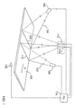
- Figure 1 shows an arrangement of the invention for inspecting the surface of an object.
- the arrangement in Figure 1 comprises two radiation sources 100 in different radiation directions 102, 104, but the radiation sources may also be located in the same radiation direction in the solution of the invention.
- the solution of the invention may also comprise only one radiation source 100.
- At least one property of the radiations directed by the radiation sources at the surface is different. Typical different properties between surface radiations include divergence, wavelength range and polarisation.
- a movement is provided between an object 106 and the arrangement for inspecting the surface of the object.
- the object 106 is moving, but the solution of the invention also allows a stationary object and a moving arrangement. It is essential that a movement is provided between the object and the arrangement.
- the radiation sources 100 use optical radiation to radiate different imaging fields 108, 100, typically equal in size, on the surface of the object 106. Naturally, at each image producing moment, the imaging field is the surface of the moving object 106.
- the solution of the invention also allows one radiation source 100 to radiate both imaging fields, which thus receive divergent radiations.
- the radiation sources are typically laser radiation sources that continuously radiate the surface of the object.
- a laser radiation source is used to radiate an area of the width of a laser line.
- An area of the width of a laser line corresponds to at least the pixel width of an image detector.
- a radiation source may comprise more than one single radiation source.
- the entire width of the surface of an object is radiated. In other words, as the object moves, its entire surface is radiated and an image produced.
- the arrangement comprises imaging field-specific image detectors 112, 114 for each imaging field 108, 110 for producing an image of the imaging fields as the movement between the object and the arrangement propagates for creating image information on the same surface area of the object at different radiations.
- the image detectors typically produce an image of the surface across the width of their pixel, i.e. one pixel-long surface areas of the moving object 106 constitute imaging fields 108, 110.
- the radiation may be processed as desired between the radiation source and the imaging field to obtain the desired radiation in the imaging field.
- the imaging field-specific detector may be a pixel matrix of a CCD camera, a pixel matrix range of the pixel matrix of a CCD camera or an image detector formed on a silicon chip.
- the aim is to inspect the entire surface of the object, which allows image detectors 112, 114 to be timed to produce an image of the radiated imaging fields 108, 110 of the object 106 such that an image is produced of the entire surface of the object to create image information.
- the image detectors may be programmed in advance to the desired image producing speed.
- the arrangement may be synchronized such that the image detector 114 produces an image of the surface area of the object 106 in its imaging field 110 at the right moment, the image detector 112 previously having produced an image of said surface area when it was in the imaging field 108.
- the arrangement may also be implemented such that the detectors take images to create image information, which is used to obtain image information on the same surface area of the object based on movement information between the object and the arrangement and/or by correlation calculation.
- Means 116 comprising a processing unit 116 are typically used to determine the above timing and synchronization of the image detectors and the image information from the same surface area of the object.
- synchronization may be implemented in image detectors 112, 114, for example.
- Control information is the basis for the comparison and/or combination of the image information on the same surface area.
- Control information is typically created based on the movement between the object 106 and the arrangement.
- Control information may also be created based on correlation calculation, image information obtained from different imaging fields 108, 110 being correlated, whereby the existence of sufficient correlation provides the image information on the same surface area of the object. Information on the movement between the object and the arrangement is not necessary in correlation calculation.
- Control information is typically used to control the movement-synchronized image information creation of the surface areas.
- Control information is used to find out image information on the same surface area of the object.
- the above measures related to control information are typically carried out with the means 116 comprising a processing unit 116.
- the processing unit is typically implemented as processor-based software, for example a computer or a processor, which uses suitable software to carry out the method steps of the invention.
- a movement sensor 118 measuring the movement of the object typically creates the movement information.
- the image information on the same surface area of the object 106 is compared and/or combined to create inspection information on the surface of the object 106 in the means 116, typically a processing unit 116 or a separate computer. Inspection information is used in the processing unit 116 or a separate computer to determine e.g. 3D properties of the surface of the object, i.e. surface roughness and colour properties, glossiness and reflectivity.
- the surface to be inspected is a band-like narrow surface or a sheet-like wide surface, such as surfaces of rolled metal products.
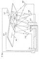
- imaging fields 200, 202, 204 on the surface of the object 106 are radiated with optical radiation such that at least two imaging fields have at least one common radiation.
- a common radiation is provided for imaging fields 200, 202 with a radiation source 206.
- a radiation is provided for imaging field 202 with a radiation source 208.
- Radiation is provided for imaging field 204 with a first radiation source 210 and a second radiation source 212.
- An image is produced of each imaging field 200, 202, 204 to its specific detector 214, 216, 218 to create image information.
- the distance between the imaging fields is typically a multiple of the size of the pixel comprised by the detector.
- image information on the surface of the object is thus created at the accuracy of a pixel.
- the processing unit 116 uses the movement information measured with the movement sensor 118 to control the image detectors to produce an image of the surface of the object at the accuracy of a pixel.
- the first preferred embodiment of the invention may be similar to the one described in Figure 1.
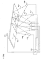
- a second embodiment of the invention shown in Figure 3 allows the colour and 3D properties of the surface of the moving object 106 to be measured with the same measurement arrangement.
- Arrow B denotes the movement of the object.
- the surface of the object is radiated with optical radiations of different colours and at different wavelengths using radiation sources 306, 308, 310 from the same radiation direction 314 to imaging fields 300, 302, 304.
- an image is produced of the imaging fields such that an image is produced of the entire surface of the object at every differently coloured radiation to create image information.
- Said image information is compared surface area-specifically for exact determination of the colour properties of the surface.
- the same arrangement also allows a 3D measurement to be carried out for example by radiating imaging fields 304, 318 with radiation sources 310, 316 whose radiation on the surface of the object is of the same colour, from two radiation directions 314, 320.
- an image is produced of the imaging fields to create image information.
- the second preferred embodiment of the invention may be similar to the one described in Figure 1.
- the surface of the moving object 106 is inspected by radiating the surface with optical radiation from three different radiation directions.
- Arrow B denotes the movement of the object.
- a radiation source 400 radiates an imaging field 402 from a first dark field radiation direction 404.
- a radiation source 412 radiates an imaging field 414 from a second dark field radiation direction 416.
- a radiation source 415 further radiates an imaging field 417 from a bright field radiation direction 419.
- the radiation sources are typically laser radiation sources that allow radiation of narrow, linear areas, called laser line areas. Radiated laser line areas are on the surface of the object at the accuracy of a pixel of the image detector.
- the third preferred embodiment of the invention may be similar to the one described in Figure 1.
- the surface of the moving object 106 is inspected on at least two different polarization levels.
- Arrow B denotes the movement of the object.
- at least two differently polarized optical radiations are used to radiate the surface of the object in different imaging fields.
- a radiation source 500 is used to radiate an imaging field 502 of the object with vertically polarized optical radiation from a bright field radiation direction 508 and a radiation source 504 is used to radiate an imaging field 506 of the object with horizontally polarized optical radiation also from the bright field radiation direction 508.
- the fourth preferred embodiment of the invention may be similar to the one described in Figure 1.
- the fourth embodiment utilizes the ratio of vertically polarized and horizontally polarized radiations, which is used to measure surface roughness, thickness and refractive index, for example.
- the thickness and refractive index of a membrane on a liquid substance, such as lacquer or oil, is measured.
Landscapes
- General Health & Medical Sciences (AREA)
- Immunology (AREA)
- Physics & Mathematics (AREA)
- Health & Medical Sciences (AREA)
- Life Sciences & Earth Sciences (AREA)
- Chemical & Material Sciences (AREA)
- Analytical Chemistry (AREA)
- Biochemistry (AREA)
- Textile Engineering (AREA)
- Engineering & Computer Science (AREA)
- General Physics & Mathematics (AREA)
- Pathology (AREA)
- Investigating Materials By The Use Of Optical Means Adapted For Particular Applications (AREA)
- Length Measuring Devices By Optical Means (AREA)
- Investigating Or Analysing Materials By Optical Means (AREA)
- Analysing Materials By The Use Of Radiation (AREA)
- Image Processing (AREA)
- Image Analysis (AREA)
Applications Claiming Priority (2)
| Application Number | Priority Date | Filing Date | Title |
|---|---|---|---|
| FI20000032 | 2000-01-07 | ||
| FI20000032A FI20000032A7 (fi) | 2000-01-07 | 2000-01-07 | Järjestely ja menetelmä pinnan tarkistamiseksi |
Publications (2)
| Publication Number | Publication Date |
|---|---|
| EP1114993A2 true EP1114993A2 (de) | 2001-07-11 |
| EP1114993A3 EP1114993A3 (de) | 2002-06-05 |
Family
ID=8556992
Family Applications (1)
| Application Number | Title | Priority Date | Filing Date |
|---|---|---|---|
| EP01660002A Withdrawn EP1114993A3 (de) | 2000-01-07 | 2001-01-05 | Verfahren und Vorrichtung zur Untersuchung von Oberflächen |
Country Status (4)
| Country | Link |
|---|---|
| US (1) | US20010015414A1 (de) |
| EP (1) | EP1114993A3 (de) |
| JP (1) | JP2001242091A (de) |
| FI (1) | FI20000032A7 (de) |
Cited By (4)
| Publication number | Priority date | Publication date | Assignee | Title |
|---|---|---|---|---|
| EP1620711A4 (de) * | 2003-04-24 | 2007-04-04 | Odyssey Developments Ltd | Überwachung der strassenreflektanz und strassenbeleuchtung |
| CN104040324A (zh) * | 2011-12-28 | 2014-09-10 | 株式会社普利司通 | 外观检查设备和外观检查方法 |
| WO2017207115A1 (en) * | 2016-05-30 | 2017-12-07 | Bobst Mex Sa | Surface inspection system and inspection method |
| CN113310441A (zh) * | 2021-06-01 | 2021-08-27 | 湖南大学 | 一种对金属表面粗糙度加工进行探测的偏振关联成像方案 |
Families Citing this family (18)
| Publication number | Priority date | Publication date | Assignee | Title |
|---|---|---|---|---|
| US7122819B2 (en) * | 2004-05-06 | 2006-10-17 | Micron Technology, Inc. | Method and apparatus for imager die package quality testing |
| US7285767B2 (en) * | 2005-10-24 | 2007-10-23 | General Electric Company | Methods and apparatus for inspecting an object |
| WO2007057993A1 (ja) * | 2005-11-21 | 2007-05-24 | Daihatsu Motor Co., Ltd. | 圧延材識別方法およびその装置 |
| US7834991B2 (en) * | 2006-07-13 | 2010-11-16 | Byk Gardner Gmbh | Determining surface properties with angle offset correction |
| FI121151B (fi) * | 2007-11-22 | 2010-07-30 | Valtion Teknillinen | Menetelmä ja laitteisto liikkuvan pinnan topografian ja optisten ominaisuuksien määrittämiseksi |
| FI20075975A7 (fi) * | 2007-12-31 | 2009-07-01 | Metso Automation Oy | Rainan mittaus |
| JP5621178B2 (ja) * | 2009-10-24 | 2014-11-05 | 株式会社第一メカテック | 外観検査装置及び印刷半田検査装置 |
| JP2011242176A (ja) * | 2010-05-14 | 2011-12-01 | Bridgestone Corp | 帯状部材の形状測定方法とその装置及び変位センサー |
| US8416409B2 (en) * | 2010-06-04 | 2013-04-09 | Lockheed Martin Corporation | Method of ellipsometric reconnaissance |
| RU2483295C2 (ru) * | 2011-02-02 | 2013-05-27 | Николай Александрович Кравцов | Способ диагностирования качества поверхностной структуры металлопроката |
| JP2013096784A (ja) * | 2011-10-31 | 2013-05-20 | Toppan Printing Co Ltd | 表面特性測定装置及びコンピュータプログラム |
| CN104297162A (zh) * | 2014-09-17 | 2015-01-21 | 宁波高新区晓圆科技有限公司 | 一种多波长多方位视觉检测方法 |
| JP6686569B2 (ja) * | 2016-03-14 | 2020-04-22 | 東芝三菱電機産業システム株式会社 | 表面疵撮影装置 |
| US10290113B2 (en) | 2016-04-08 | 2019-05-14 | Nippon Steel & Sumitomo Metal Corporation | Surface state monitoring apparatus for metallic body and surface state monitoring method for metallic body |
| KR102484352B1 (ko) * | 2016-08-18 | 2023-01-04 | 한화정밀기계 주식회사 | 부품 실장기의 카메라 모듈 |
| JP6149990B2 (ja) * | 2016-09-02 | 2017-06-21 | Jfeスチール株式会社 | 表面欠陥検出方法及び表面欠陥検出装置 |
| JP6683088B2 (ja) * | 2016-09-23 | 2020-04-15 | 日本製鉄株式会社 | 表面性状検査装置、表面性状検査方法及びプログラム |
| DE102022002963B4 (de) * | 2022-08-16 | 2024-08-22 | Baumer lnspection GmbH | Optische Prüfvorrichtung und Prüfverfahren |
Family Cites Families (4)
| Publication number | Priority date | Publication date | Assignee | Title |
|---|---|---|---|---|
| DE2612482A1 (de) * | 1976-03-24 | 1977-10-06 | Hoesch Werke Ag | Verfahren und einrichtung zur optischen beobachtung der oberflaeche von schnell bewegtem walzmaterial |
| DE19720308C2 (de) * | 1997-05-15 | 1999-05-20 | Parsytec Computer Gmbh | Vorrichtung zur kontinuierlichen Detektion von Fehlern nach Größe und Art auf der Oberfläche eines bewegten Materials |
| ATE197503T1 (de) * | 1997-08-22 | 2000-11-11 | Fraunhofer Ges Forschung | Verfahren und vorrichtung zur automatischen prüfung bewegter oberflächen |
| AT406528B (de) * | 1998-05-05 | 2000-06-26 | Oesterr Forsch Seibersdorf | Verfahren und einrichtung zur feststellung, insbesondere zur visualisierung, von fehlern auf der oberfläche von gegenständen |
-
2000
- 2000-01-07 FI FI20000032A patent/FI20000032A7/fi unknown
-
2001
- 2001-01-05 EP EP01660002A patent/EP1114993A3/de not_active Withdrawn
- 2001-01-05 US US09/754,214 patent/US20010015414A1/en not_active Abandoned
- 2001-01-09 JP JP2001001777A patent/JP2001242091A/ja not_active Withdrawn
Cited By (9)
| Publication number | Priority date | Publication date | Assignee | Title |
|---|---|---|---|---|
| EP1620711A4 (de) * | 2003-04-24 | 2007-04-04 | Odyssey Developments Ltd | Überwachung der strassenreflektanz und strassenbeleuchtung |
| CN104040324A (zh) * | 2011-12-28 | 2014-09-10 | 株式会社普利司通 | 外观检查设备和外观检查方法 |
| EP2799848A4 (de) * | 2011-12-28 | 2015-08-12 | Bridgestone Corp | Prüfvorrichtung mit externer ansicht und prüfverfahren mit externer ansicht |
| US9310278B2 (en) | 2011-12-28 | 2016-04-12 | Bridgestone Corporation | Appearance inspection apparatus and appearance inspection method with uneveness detecting |
| CN104040324B (zh) * | 2011-12-28 | 2016-06-29 | 株式会社普利司通 | 外观检查设备和外观检查方法 |
| WO2017207115A1 (en) * | 2016-05-30 | 2017-12-07 | Bobst Mex Sa | Surface inspection system and inspection method |
| US11169095B2 (en) | 2016-05-30 | 2021-11-09 | Bobst Mex Sa | Surface inspection system and method using multiple light sources and a camera offset therefrom |
| CN113310441A (zh) * | 2021-06-01 | 2021-08-27 | 湖南大学 | 一种对金属表面粗糙度加工进行探测的偏振关联成像方案 |
| CN113310441B (zh) * | 2021-06-01 | 2022-06-10 | 湖南大学 | 一种对金属表面粗糙度加工进行探测的偏振关联成像方法 |
Also Published As
| Publication number | Publication date |
|---|---|
| FI20000032A0 (fi) | 2000-01-07 |
| JP2001242091A (ja) | 2001-09-07 |
| EP1114993A3 (de) | 2002-06-05 |
| FI20000032A7 (fi) | 2001-10-26 |
| US20010015414A1 (en) | 2001-08-23 |
Similar Documents
| Publication | Publication Date | Title |
|---|---|---|
| EP1114993A2 (de) | Verfahren und Vorrichtung zur Untersuchung von Oberflächen | |
| US6064478A (en) | Method of and apparatus for automatic detection of three-dimensional defects in moving surfaces by means of color vision systems | |
| US11619485B2 (en) | Hybrid 3D optical scanning system | |
| US7471383B2 (en) | Method of automated quantitative analysis of distortion in shaped vehicle glass by reflected optical imaging | |
| US7511293B2 (en) | Scatterometer having a computer system that reads data from selected pixels of the sensor array | |
| CN101819165B (zh) | 用于检测图案化基板的缺陷的方法及系统 | |
| US7382457B2 (en) | Illumination system for material inspection | |
| CN116840260B (zh) | 晶圆表面缺陷检测方法及装置 | |
| KR101595581B1 (ko) | 반사 특성을 가진 물체의 밀리미터 또는 밀리미터 이하의 상세 구조를 관측하기 위한 광학 장치 | |
| HU229699B1 (hu) | Pinhole kamerát alkalmazó, leképzõ optikai vizsgálóberendezés (reflektométer, polariméter, ellipszométer) | |
| Wang et al. | Online detection technique of 3D defects for steel strips based on photometric stereo | |
| CA2334225C (en) | Method and device for opto-electrical acquisition of shapes by axial illumination | |
| US8363903B2 (en) | Method and apparatus for determining the topography and optical properties of a moving surface | |
| US6930770B2 (en) | High throughput inspection system and method for generating transmitted and/or reflected images | |
| CN107329373B (zh) | 一种套刻误差测量装置及方法 | |
| US20210310799A1 (en) | Apparatus, measurement system and method for capturing an at least partially reflective surface using two reflection patterns | |
| US20150212009A1 (en) | Method and device for identifying materials in a scene | |
| JPS58204353A (ja) | 金属物体表面探傷方法 | |
| US5321495A (en) | Optical detecting system for determining particle position on a substrate | |
| US3322024A (en) | Optical method for the inspection of a transparent object for deffects including comparing light energy at two stations | |
| JP2001201323A (ja) | 溝の深さ測定方法及び測定装置 | |
| CN219829789U (zh) | 一种兼顾高亮表面和粗糙表面的线激光轮廓仪 | |
| RU2535519C2 (ru) | Способ бесконтактного измерения параметров шероховатости поверхности | |
| JPS6117281B2 (de) | ||
| GB2588991A (en) | Optical property measurement using a sensor behind a display screen |
Legal Events
| Date | Code | Title | Description |
|---|---|---|---|
| PUAI | Public reference made under article 153(3) epc to a published international application that has entered the european phase |
Free format text: ORIGINAL CODE: 0009012 |
|
| AK | Designated contracting states |
Kind code of ref document: A2 Designated state(s): AT BE CH CY DE DK ES FI FR GB GR IE IT LI LU MC NL PT SE TR |
|
| AX | Request for extension of the european patent |
Free format text: AL;LT;LV;MK;RO;SI |
|
| PUAL | Search report despatched |
Free format text: ORIGINAL CODE: 0009013 |
|
| AK | Designated contracting states |
Kind code of ref document: A3 Designated state(s): AT BE CH CY DE DK ES FI FR GB GR IE IT LI LU MC NL PT SE TR |
|
| AX | Request for extension of the european patent |
Free format text: AL;LT;LV;MK;RO;SI |
|
| 17P | Request for examination filed |
Effective date: 20021122 |
|
| AKX | Designation fees paid |
Designated state(s): AT BE CH CY DE DK ES FI FR GB GR IE IT LI LU MC NL PT SE TR |
|
| STAA | Information on the status of an ep patent application or granted ep patent |
Free format text: STATUS: THE APPLICATION HAS BEEN WITHDRAWN |
|
| 18W | Application withdrawn |
Effective date: 20030802 |