EP1115216A1 - Recepteur et procede d'egalisation adaptative - Google Patents
Recepteur et procede d'egalisation adaptative Download PDFInfo
- Publication number
- EP1115216A1 EP1115216A1 EP00939053A EP00939053A EP1115216A1 EP 1115216 A1 EP1115216 A1 EP 1115216A1 EP 00939053 A EP00939053 A EP 00939053A EP 00939053 A EP00939053 A EP 00939053A EP 1115216 A1 EP1115216 A1 EP 1115216A1
- Authority
- EP
- European Patent Office
- Prior art keywords
- reliability information
- reliability
- timing
- decision
- unit
- Prior art date
- Legal status (The legal status is an assumption and is not a legal conclusion. Google has not performed a legal analysis and makes no representation as to the accuracy of the status listed.)
- Withdrawn
Links
Images









Classifications
-
- H—ELECTRICITY
- H04—ELECTRIC COMMUNICATION TECHNIQUE
- H04B—TRANSMISSION
- H04B7/00—Radio transmission systems, i.e. using radiation field
- H04B7/005—Control of transmission; Equalising
-
- H—ELECTRICITY
- H04—ELECTRIC COMMUNICATION TECHNIQUE
- H04L—TRANSMISSION OF DIGITAL INFORMATION, e.g. TELEGRAPHIC COMMUNICATION
- H04L25/00—Baseband systems
- H04L25/02—Details ; arrangements for supplying electrical power along data transmission lines
- H04L25/03—Shaping networks in transmitter or receiver, e.g. adaptive shaping networks
- H04L25/03006—Arrangements for removing intersymbol interference
- H04L25/03012—Arrangements for removing intersymbol interference operating in the time domain
- H04L25/03019—Arrangements for removing intersymbol interference operating in the time domain adaptive, i.e. capable of adjustment during data reception
- H04L25/03038—Arrangements for removing intersymbol interference operating in the time domain adaptive, i.e. capable of adjustment during data reception with a non-recursive structure
- H04L25/0305—Arrangements for removing intersymbol interference operating in the time domain adaptive, i.e. capable of adjustment during data reception with a non-recursive structure using blind adaptation
-
- H—ELECTRICITY
- H04—ELECTRIC COMMUNICATION TECHNIQUE
- H04L—TRANSMISSION OF DIGITAL INFORMATION, e.g. TELEGRAPHIC COMMUNICATION
- H04L25/00—Baseband systems
- H04L25/02—Details ; arrangements for supplying electrical power along data transmission lines
- H04L25/06—DC level restoring means; Bias distortion correction ; Decision circuits providing symbol by symbol detection
- H04L25/068—DC level restoring means; Bias distortion correction ; Decision circuits providing symbol by symbol detection by sampling faster than the nominal bit rate
-
- H—ELECTRICITY
- H04—ELECTRIC COMMUNICATION TECHNIQUE
- H04B—TRANSMISSION
- H04B7/00—Radio transmission systems, i.e. using radiation field
- H04B7/02—Diversity systems; Multi-antenna system, i.e. transmission or reception using multiple antennas
- H04B7/04—Diversity systems; Multi-antenna system, i.e. transmission or reception using multiple antennas using two or more spaced independent antennas
- H04B7/08—Diversity systems; Multi-antenna system, i.e. transmission or reception using multiple antennas using two or more spaced independent antennas at the receiving station
- H04B7/0837—Diversity systems; Multi-antenna system, i.e. transmission or reception using multiple antennas using two or more spaced independent antennas at the receiving station using pre-detection combining
- H04B7/0842—Weighted combining
- H04B7/0845—Weighted combining per branch equalization, e.g. by an FIR-filter or RAKE receiver per antenna branch
-
- H—ELECTRICITY
- H04—ELECTRIC COMMUNICATION TECHNIQUE
- H04L—TRANSMISSION OF DIGITAL INFORMATION, e.g. TELEGRAPHIC COMMUNICATION
- H04L25/00—Baseband systems
- H04L25/02—Details ; arrangements for supplying electrical power along data transmission lines
- H04L25/03—Shaping networks in transmitter or receiver, e.g. adaptive shaping networks
- H04L25/03006—Arrangements for removing intersymbol interference
- H04L25/03178—Arrangements involving sequence estimation techniques
-
- H—ELECTRICITY
- H04—ELECTRIC COMMUNICATION TECHNIQUE
- H04L—TRANSMISSION OF DIGITAL INFORMATION, e.g. TELEGRAPHIC COMMUNICATION
- H04L7/00—Arrangements for synchronising receiver with transmitter
- H04L7/04—Speed or phase control by synchronisation signals
- H04L7/08—Speed or phase control by synchronisation signals the synchronisation signals recurring cyclically
Definitions
- This invention in general relates to a receiver to be used for a mobile phone or the like. More specifically, this invention relates to the receiver and an adaptive equalizer method in the receiver which judges data without utilizing a training sequence for an operation of an adaptive equalizer.
- a conventional receiver and adaptive equalizer method will be explained below.
- a non-ignorable delay wave is occasionally generated in a data symbol due to multipath propagation. If such a delay wave is generated, interference occurs between code symbols. This phenomenon is called as inter-symbol interference.
- an equalizing technique for example, exists as a receiving technique which overcomes the inter-symbol interference.
- Fig. 20 shows a structure of an adaptive equalizer adopted by a conventional receiver.
- legend 1 denotes a received signal input terminal
- legend 2 denotes a decision value output terminal
- legend 3 denotes an over-sample sampler
- legend 100 denotes a symbol rate data output circuit
- legend 101 denotes a timing detector utilizing a training sequence
- legend 102 denotes an equalizer utilizing a training sequence.
- Fig. 21 is a diagram showing a principle of an over-sample by the receiver.
- Fig. 21 shows an example of 8-time over-sample, namely, the case where sampling is performed eight times with 1 symbol cycle.
- sampling time is represented by integer numbers
- over-sample timing numbers corresponding to the sampling time are represented by eight numbers from '0' to '7'. Namely, in a sequence where the over-sample timing number is "1", data of time '9' are output as symbol data next to time '1'.
- data of time '5' are output as over-sample data as symbol data next to time '1' in a sequence where the over-sample timing number is '1'.
- a received sequence will be explained as symbol rate data, but over-sample data can be treated by similar concept.
- a received signal is first sampled at predetermined timing by the over-sample sampler 3.
- the timing detector 101 receives the over-sampled received signal and determines over-sample timing numbers shown in Fig. 21 by utilizing a training sequence which is a known pattern.
- the symbol rate data output circuit 100 receives the over-sample timing number, and outputs a received sequence of a symbol rate corresponding to this number.
- the equalizer 102 utilizing a training sequence receives the received sequence of the symbol rate, and creates a decision value which is an estimated value of a transmission data sequence so as to output the decision value from the decision value output terminal 2.
- the receiver which uses the equalizer 102 utilizing a training sequence, once estimates a position of a training sequence in any manner so as to operate.
- an equalizer which does not require a training sequence exists. This is called as a blind equalizer (for example, described in "Linear Equalization Theory" written by Yoichi Sato, Maruzen, 1990). Since a blind equalizer operates without utilizing a training sequence, the above-mentioned process utilizing training can be avoided.
- Fig. 22 shows a structure of a conventional receiver using a blind equalizer described in "Synchronization Establishing System for Equalizer” written by Masaaki Fujii (Japanese Patent Application Laid-Open No. 6-216810 (1994)).
- Fig. 22 shows a structure of a conventional receiver using a blind equalizer described in "Synchronization Establishing System for Equalizer” written by Masaaki Fujii (Japanese Patent Application Laid-Open No. 6-216810 (1994)).
- legend 1 denotes a received signal input terminal
- legend 2 denotes a decision value output terminal
- legend 3 denotes an over-sample sampler
- legend 4 denotes a received signal storage circuit
- legend 102 denotes an equalizer utilizing a training sequence
- legends 103A, 103B and 103C denote blind equalizers with UW (unique word) detecting function
- legend 104 denotes a UW portion error comparing circuit
- legend 105 denotes an optimum phase selecting circuit.
- UW unique word
- Fig. 23 shows an example of the structure of the blind equalizer 103 with UW detecting function shown in Fig. 22.
- legend 7 denotes a UW detector
- legend 8 denotes a received sequence input terminal
- legend 13 denotes a blind equalizer
- legend 107 denotes an error output terminal
- legend 108 denotes a mask circuit.
- a received signal which is over-sampled by the over-sample sampler 3, is once stored in the received signal storage circuit 4.
- the received signal storage circuit 4 outputs an N-systemic received sequence, shown in Fig. 21, where over-sample timing number differs, and N-numbered blind equalizers 103A, 103B, ... , 103C with UW detecting function receive received signals respectively.
- the blind equalizer 13 which received the received sequence outputs a decision value and an error value.
- the UW detector 7 receives the decision value so as to detect UW and instructs the mask circuit 108 on mask for mask period other than UW detection time.
- the mask circuit 108 outputs an error value which was received except at mask instructing period.
- the UW portion error comparing circuit 104 receives N-numbered pieces of error information from the N-numbered blind equalizers 103 with UW detecting function, and outputs timing corresponding to a received sequence where the error is the smallest.
- the optimum phase selecting circuit 105 selects a received sequence of a symbol rate from the received signal storage circuit 4 according to the timing instruction from the UW portion error comparing circuit 104, and outputs the received sequence.
- the equalizer 102 receives the received sequence, and performs an adaptive equalizer process utilizing a training sequence so as to output a decision value from the decision value output terminal 2.
- the present invention is devised in order to solve the above problems . It is an object of the present invention to provide a receiver which is capable of reproducing stable timing even in the environment of inter-symbol interference and outputting a decision value in an adaptive equalizer process only using a blind equalizer without utilizing a training sequence, and relates to an adaptive equalizer method in the receiver.
- a receiver of the present invention having an adaptive equalizer which judges a transmission data sequence by means of an adaptive equalizer process comprises a sampling unit which samples a received signal at a speed of not less than a symbol rate; a signal sequence distributing unit which distributes the sampled signal to at least one signal sequence with different sampling timing; a plurality of blind equalization units with reliability information which output decision values (symbol sequences) and their reliability information correspondingly to the respective signal sequences without utilizing a training sequence; and a decision value selecting unit which selects an optimum decision value based on the plural pieces of reliability information.
- the sampling unit samples a received signal at a speed of not less than a symbol rate
- the signal sequence distributing unit distributes the sampled signal sequence to sequences with different over-sample timing numbers.
- the blind equalization unit with reliability information receive the distributed signal sequences and perform the adaptive equalizer process so as to output decision data and reliability information.
- the decision value selecting unit receives plural pieces of reliability information and the decision data so as to output the decision data with the highest reliability as a decision value.
- the blind equalization unit with reliability information include a blind equalization unit which outputs soft decision values to which reliability for each symbol is added; and a reliability accumulation unit which receives the soft decision values per symbol and outputs a cumulative value of the reliabilities as reliability information.
- the blind equalization unit receive the received sequence and outputs soft decision values which are obtained by adding reliability components of each symbol are added to the decision values.
- the reliability accumulation unit accumulates the reliabilities of each symbol of the soft decision values so as to output reliability information.
- the reliability information when a lot of reliability components exist in the soft decision values, the reliability information as the cumulative value show a large value.
- the blind equalization unit with reliability information include a blind equalization unit which receives the signal sequence and outputs square errors which are generated when data are judged as well as the decision values; and a reliability accumulation unit which outputs a cumulative value of the square errors as reliability information.
- the blind equalization unit receive the received sequence and output square errors which are generated when data are judged as well as the decision values.
- the reliability accumulation unit accumulates the square errors so as to output the cumulative value.
- the reliability becomes higher.
- a frequency deviation addition unit which adds a frequency deviation is provided at a stage before the blind equalization unit with reliability information.
- the frequency deviation addition unit gives different frequency deviations to the received sequences to be supplied to the blind equalization unit with reliability information so that selection of decision data is effective even at the same over-sample timing number.
- a synchronization judging unit which performs unique word detection in order to obtain synchronization utilizing the decision values output by the plurality of blind equalization units with reliability information so as to detect as to whether being in a synchronous state or in an asynchronous state, is provided.
- a receiver of next invention having an adaptive equalizer which judges a transmission data sequence by means of an adaptive equalizer process comprises a sampling unit which samples a received signal at a speed of not less than a symbol rate; a signal storage unit which stores the sampled signal; a blind equalization unit with reliability information which receive a signal sequence from the signal storage unit and outputs decision values and their reliability information without utilizing a training sequence operating at a clock faster than a signal sequence cycle; and a timing control unit which controls time at which the signal sequence is output and operation time of the blind equalization unit with reliability information so as to output decision data with the highest reliability as decision values.
- the sampling unit samples a received signal at a speed of not less than a symbol rate
- the signal storage unit stores the over-sampled received signal.
- an over-sample timing number indicated by the operation timing control unit is output at specified timing and at a speed faster than the symbol rate.
- the blind equalization unit with reliability information receives a received sequence at a speed faster than a symbol rate and outputs reliability information and decision data.
- the blind equalization unit with reliability information includes a blind equalization unit which outputs soft decision values to which reliability for each symbol is added; and a reliability accumulation unit which receives the soft decision values per symbol and outputs a cumulative value of the reliability as reliability information.
- the blind equalization unit receives a received sequence and outputs soft decision values which are obtained by adding reliability components of each symbol to the decision values.
- the reliability accumulation unit accumulates the reliabilities of each symbol of the soft decision values so as to output reliability information.
- the reliability information when a lot of reliability components exist in the soft decision values, the reliability information as the cumulative value shows a large value.
- the blind equalization unit with reliability information includes a blind equalization unit which receives the signal sequence and outputs square errors which are generated when data are judged as well as the decision values; and a reliability accumulation unit which outputs a cumulative value of the square errors as reliability information.
- the blind equalization unit receives a received sequence, and outputs square errors which are generated when data are judged as well as the decision values.
- the reliability accumulation unit accumulates the square errors so as to output the cumulative value.
- the reliability becomes higher.
- a frequency deviation addition unit which adds a frequency deviation is provided at a stage before the blind equalization unit with reliability information.
- the frequency deviation addition unit gives different frequency deviations to received sequences to be supplied to the blind equalization unit with reliability information so that selection of the decision data is effective even at the same over-sample timing number.
- length of a channel memory which is a parameter of the blind equalization unit with reliability information and the frequency deviation can be controlled.
- the timing control unit forcibly changes a channel memory length which is a parameter of the blind equalization unit with reliability information and frequency deviations given by the frequency deviation addition unit.
- a synchronization judging unit which performs unique word detection in order to obtain synchronization using the decision values and making a judgment as to whether being in a synchronous state or in an asynchronous state, is provided.
- the synchronization judging unit makes a judgment as to where the receiver is in a synchronous state or in an asynchronous state by utilizing the decision values. As a result, the over-sample timing number of the signal sequence is changed. For example, when the synchronization is not established, intervals between the over-sample timing numbers are distributed thoroughly. Meanwhile, when the synchronization is established, the intervals between the over-sample timing numbers are set finely so that accuracy of the timing synchronization is heightened.
- a synchronization judging unit which performs unique word detection in order to obtain synchronization for each of the blind equalization units with reliability information and making a judgment as to whether being in a synchronous state or in an asynchronous state individually, is provided.
- Each synchronization judging unit per forms unique word detection on the decision data output by the blind equalization unit with reliability information, and outputs the detected results and detection timing. Further, the decision value selecting unit selects a decision value using not only the reliability information but also the unique word detected results and detection timing.
- a reproduction timing generating unit which generates a reproduction timing signal based on timing information including output timing of the optimum decision value and the unique word detected result, is provided.
- the decision value selecting unit creates timing information including the finally selected timing and unique word detected result. Further, the reproduction timing generating unit outputs a reproduction timing signal based on the timing information to be a reference.
- a reproduction timing generating unit which generates a reproduction timing signal based on timing information including output timing of the optimum decision value and the unique word detected result, is provided.
- the decision value selecting unit generates timing information including the finally selected timing and unique word detected result. Further, the reproduction timing generating unit outputs a reproduction timing signal based on the timing information to be a reference.
- a reproduction timing generating unit which generates a reproduction timing signal based on timing information including output timing of the decision value and the unique word detected result, is provided.
- the timing control unit generates timing information including the finally selected timing and unique word detected result. Further, the reproduction timing generating unit outputs a reproduction timing signal based on the timing information to be a reference.
- sampling unit samples a plurality of received signals individually at a speed of not less than a symbol rate.
- a plurality of sampling unit are provided, and a frequency of an operation clock of the blind equalization unit with reliability information is given so that a plurality of different received signals are processed.
- a received signal is sampled at a speed of not less than a symbol rate by the sampling step.
- the sampled signal sequence is distributed to sequences with different over-sample timing numbers.
- the decision value/reliability information output step the distributed signal sequences, and decision data and reliability information are output by executing an adaptive equalizer process.
- the decision value selecting step a plural pieces of reliability information and decision data are received, and the decision data with the highest reliability are output as a decision value.
- the decision value/reliability information output step includes the soft decision value output step of outputting soft decision values to which reliability of each symbol is added; and the reliability cumulative step receiving the soft decision values of each symbol so as to output a cumulative value of the reliabilities as reliability information.
- the soft decision value output step soft decision values which are obtained by adding reliability components of each symbol to the decision values are output, and at the reliability cumulative step, the reliabilities of each symbol of the soft decision values are cumulated so that the reliability information is output.
- the reliability information as the cumulative value shows a large value.
- the decision value/reliability information output step includes the square error output step of receiving the signal sequence and outputs square errors which are generated when data are judged as well as the decision values; and the reliability cumulative step of outputting a cumulative value of the square errors as reliability information.
- the decision value/reliability information output step square errors which are generated when data are judged as well as the decision values are output, and at the reliability cumulative step, the square errors are cumulated so that the cumulative value is output.
- the square error cumulative value is smaller, its reliability becomes higher.
- the frequency deviation adding step of adding a frequency deviation is provided before the decision value/reliability information output step is executed.
- the synchronization judging step of performing unique word detection in order to obtain synchronization using the plural decision values and making a judgment as to whether or not being in a synchronous state or in an asynchronous state is provided.
- the synchronous state is obtained.
- the two unique words are detected and a number of symbols of the unique words does not match with the known value, or when one unique words is not detected, the asynchronous state is obtained.
- a received signal is sampled at a speed of not less than a symbol rate by the sampling step.
- the received signal over-sampled is stored at the signal storage step.
- an over-sample timing number which is indicated at the operation timing control step is output at specified timing and at a speed faster than the symbol rate.
- a received sequence is received at a speed faster than the symbol rate, and reliability information and decision data are output.
- the decision value/reliability information output step includes the soft decision value output step of outputting soft decision values to which reliability of each symbol is added; and the reliability cumulative step of receiving the soft decision values of each symbol and outputs a cumulative value of the reliabilities as reliability information.
- the soft decision value output step soft decision values which are obtained by adding reliability components of each symbol to the decision values are output.
- the reliability cumulative step the reliabilities of each symbol of the soft decision values are cumulated so that the reliability information is output.
- the reliability information as the cumulative value shows a large value.
- the decision value/reliability information output step includes the square error output step of receiving the signal sequence and outputs square errors which are generated when data are judged as well as the decision values; and the reliability cumulative step of a cumulative value of the square errors as reliability information.
- the reliability cumulative step the square errors are cumulated so that the cumulative value is output.
- the square error cumulative value is smaller, its reliability becomes higher.
- the frequency deviation adding step of adding a frequency deviation is provided before the decision value/reliability information output step is executed.
- length of channel memory which is a parameter at the decision value/reliability information output step and the frequency deviation can be controlled.
- channel memory length which is aparameter of the decision value/reliability information output step and the frequency deviations given at the frequency deviation adding step are changed forcibly.
- the synchronization judging step of performing unique word detection in order to obtain synchronization utilizing the decision values and making a judgment as to being in a synchronous state or in an asynchronous state is provided.
- the synchronization judging step a judgment is made as to whether the receiver is in a synchronous state or in an asynchronous state by utilizing the decision values.
- the over-sample timing number of the signal sequence is changed. For example, when the synchronization is not established, intervals between the over-sample timing numbers are distributed thoroughly, whereas when the synchronization is established, the intervals between the over-sample timing numbers are set finely so that the accuracy of timing synchronization is heightened.
- the synchronization judging step of performing unique word detection in order to obtain synchronization in the unit of the decision value/reliability information output step of outputting the decision values and their reliabilities and making a judgment as to whether being in a synchronous state or in an asynchronous state is provided.
- the synchronization judging step unique words are detected based on the decision data output from the plural blind equalization units, and the detected results and detection timing are output. Further, at the decision value selecting step, the decision value is selected by using not only the reliability information but also the unique word detected results and the detection timing.
- the reproduction timing generating step of generating a reproduction timing signal based on timing information including output timing of the optimum decision value and the unique word detected result is provided.
- timing information including finally selected timing and the unique word detected results is generated. Further, at the reproduction timing generating step, a reproduction timing signal is output based on the timing information to be a reference.
- the reproduction timing generating step of generating a reproduction timing signal based on timing information including output timing of the optimum decision value and the unique word detected result is provided.
- timing information including finally selected timing and the unique word detected results is generated. Further, at the reproduction timing generating step, a reproduction timing signal is output based on the timing information to be a reference.
- the reproduction timing generating step of generating a reproduction timing signal based on timing information including output timing of the decision values and the unique word detected result is provided.
- timing information including finally selected timing and the unique word detected results is generated. Further, at the reproduction timing generating step, a reproduction timing signal is output based on the timing information to be a reference.
- the sampling step samples a plurality of received signals at a speed of not less than a symbol rate individually.
- a plurality of received signals are sampled individually, and frequencies of an operation clock of the blind equalizers are given sot hat the plural different received signal are processed.
- Fig. 1 shows a structure of a receiver according to a first embodiment of the present invention
- Fig. 2 is a diagram showing a structural example of a blind equalizer with reliability information
- Fig. 3 is a diagram showing a structural example of a blind equalizer with reliability information different from Fig. 2
- Fig. 4 shows a structure of a blind equalizer with reliability information different from Fig. 2 and Fig. 3
- Fig. 5 shows a structure of the receiver according to a second embodiment of the present invention
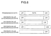
- Fig. 6 is a diagram for explaining a synchronous/asynchronous state
- Fig. 7 is a diagram showing over-sample timing numbers under a condition that synchronization is not established
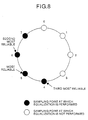
- Fig. 8 is over-sample timing numbers which are changed by a received signal output circuit
- Fig. 9 is a diagram showing a state that reliability of the over-sampling timing numbers changes
- Fig. 10 is a diagram showing changed over-sample timing numbers when the reliability of the over-sample timing numbers changes
- Fig. 11 shows a structure of the receiver according to a third embodiment of the present invention
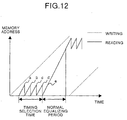
- Fig. 12 is a diagram showing a relationship between a writing process and a reading process when a dual port RAM is imaged as a received signal storage circuit
- Fig. 13 is a diagram showing a structural example of a blind equalizer with reliability information different from Fig. 2 and Fig. 3
- Fig. 14 shows a structure of the receiver according to a fourth embodiment of the present invention
- Fig. 15 shows a structure of the receiver according to a fifth embodiment of the present invention
- Fig. 16 shows a structure of the receiver according to a sixth embodiment of the present invention
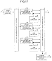
- Fig. 17 shows a structure of the receiver according to a seventh embodiment of the present invention
- Fig. 18 shows a structure of the receiver according to an eighth embodiment of the present invention
- Fig. 19 shows a structure of the receiver according to a ninth embodiment of the present invention
- Fig. 20 shows a structure of an adaptive equalizer adopted in a conventional receiver
- Fig. 21 is a diagram showing a principle of the over-sample by the receiver
- Fig. 22 shows a structure of a conventional receiver
- Fig. 23 shows a structure of a blind equalizer with UW detecting function.
- Fig. 1 shows a structure of the receiver according to a first embodiment of the present invention.
- legend 1 denotes a received signal input terminal
- legend 2 denotes a decision value output terminal
- legend 3 denotes an over-sample sampler
- legend 4 denotes a received sequence output circuit
- legends 5A, 5B, 5C, ... denote blind equalizers with reliability information
- legend 6 denotes a decision data selecting circuit.
- Fig. 2 is a diagram showing a structural example of the blind equalizer with reliability information.
- legend 8 denotes a received sequence input terminal
- legend 9 denotes a decision data output terminal
- legend 10 denotes a reliability information output terminal
- legend 11 denotes a soft decision output blind equalizer
- legend 12 denotes a reliability component accumulation circuit.
- Fig. 3 is a diagram showing a structural example of the blind equalizer with reliability information different from Fig. 2.
- legend 13 denotes a blind equalizer
- legend 14 denotes a square error cumulative circuit.
- the same legends are provided to the components which are the same as those in Fig. 2 explained above, and the description thereof is omitted.
- a received signal is sampled by the over-sample sampler 3 at a speed of not less than a symbol rate.
- the received sequence output circuit 4 distributes the over-sampled received signal as aplurality of received sequences to sequences with different over-sample timing numbers.
- signal sequences of the same sampling timing are occasionally allowed to exist.
- the N-numbered blind equalizers 5A to 5C with reliability information receive the received sequences individually from the received sequence output circuit 4, and perform an adaptive equalizer process without utilizing a training sequence, and outputs decision data and reliability information.
- the reliability information does not represent reliability per symbol such as soft decision values but represents reliability of whole data sequence.
- the blind equalizers with reliability information a number of which is the same as a number of signal sequences with different sampling timing or is larger than this number.
- the decision data selecting circuit 6 receives N-numbered pieces of reliability information and decision data, and outputs decision data output by the blind equalizer with the highest reliability information as a decision value.
- the present embodiment has the above structure so that data can be judged stably without utilizing a training sequence.
- a method of realizing the blind equalizer is detailed in, for example, "Adaptive maximum-likelihood sequence estimation by means of combined equalization and decoding in fading environments" written by H. Kubo and the others (IEEE JSAC, pp. 102-109, 1995).
- Fig. 2 shows amethod of realizing the blind equalizers with reliability information 5A to 5C shown in Fig. 1.
- a method of realizing the soft decision output blind equalizer 11 is detailed in, for example, "An Adaptive Soft-Output Viterbi Equalizer for Fast Time-Varying Frequency Selective Fading" by Nagayasu et. al., (literature of IEICE B-II, pp.397-386, 1997).
- multiplex differential detection which is one kind of differential detection (including differential detection) can be treated as one example of the blind equalizer.
- the soft decision output blind equalizer 11 shown in Fig. 2 receives a received sequence, and outputs soft decision values which are obtained by adding reliability components for respective symbols to decision values.
- the reliability component accumulation circuit 12 accumulates reliability for each symbol of the soft decision values and outputs reliability information. Namely, when a lot of reliability components exist in the soft decision values, the reliability information which are the cumulative value of the reliability components show a large value.
- Fig. 3 shows another method of realizing the blind equalizers with reliability information 5A and 5B in Fig. 3.
- the blind equalizer 13 receives a received sequence and outputs a square error (for example, a metric normalized value of a Viterbi equalizer) which is generated when data are judged as well as a decision value.
- a square error for example, a metric normalized value of a Viterbi equalizer
- the blind equalizer 13 when the blind equalizer 13 operates based on a Viterbi algorithm, an operation for normalizing each symbol time using the smallest path metric (square error) is utilized, and the smallest path metric is to be a square error which is used in the square error cumulative circuit 14. Therefore, the square error cumulative circuit 14 accumulates the square errors so as to output it.
- the square error cumulative value is smaller, its reliability is higher.
- the received sequence output circuit 4 normally outputs received signals of different over-sample timing numbers to the respective blind equalizers with reliability information 5.
- Fig. 4 shows a structure of the blind equalizer with reliability information different from Fig. 2 and Fig. 3.
- legend 5 denotes the aforementioned blind equalizer with reliability information of Fig. 2 or Fig. 3
- legend 8 denotes the symbol rate received sequence input terminal
- legend 9 denotes the decision data output terminal
- legend 10 denotes the reliability information output terminal
- legend 16 denotes a fixed frequency addition circuit.
- the fixed frequency deviation addition circuit 16 gives a different frequency deviation to a received sequence to be supplied to the blind equalizer with reliability information 5
- selection of decision data is effective even with the same over-sample timing number.
- the fixed frequency deviation addition circuit 16 is provided at a stage before the blind equalizer with reliability information 5 so that a forced frequency deviation is given. This process enables an amount of frequency deviation capable of being demodulated to be increased.
- a decision value in the adaptive equalizer process can be output only by the process using the blind equalizers with reliability information.
- Fig. 5 shows a structure of the receiver according to a second embodiment of the present invention.
- the same legends are provided to the components which are the same as those in the aforementioned first embodiment, and the description thereof is omitted.
- legend 7 denotes a UW (unique word) detector.
- the operation which is the same as that in the first embodiment is performed basically, but a difference with the first embodiment is that, for example, the UW detector 7 performs UW detection utilizing a decision value and makes a judgment as to whether the receiver is in a synchronous state or in an asynchronous state.
- the present embodiment is characterized in that the over-sample timing number of the received sequence output by the received signal output circuit 4 is changed by the judging process.
- Fig. 6 is a diagram for explaining a synchronous/asynchronous state based on a relationship between transmission data and a decision value. For example, when two UWs are detected from the decision value and a number of symbols between UWs matches with a known value (a number of data symbols in the drawing), the receiver is in the synchronous state. Meanwhile, when two UWs are detected and a number of symbols between UWs is different from a known value, or when one UW cannot be detected, the receiver is in the asynchronous state. In the present embodiment, data which are judged as in the asynchronous state are not selected as decision data so that accuracy of a decision value is heightened.
- Fig. 7 shows over-sample timing numbers under a condition that synchronization is not established. Since synchronization is not established, the over-sample timing numbers '0', '2', '4' and '6' are selected uniformly, for example.
- the over-sample timing number '6' is the most reliable and the over-sample timing number '4' is the second most reliable
- the over-sample timing number is changed into '4', '5', '6' and '7'' for example, namely, timing at which the reliability is estimated to be high with reference to the reliability of Fig. 7.
- Fig. 8 shows over-sample timing numbers which are changed by the received signal output circuit 4 after synchronization is established.
- the over-sample timing number '5' is most reliable
- the over-sample timing number '6' is second most reliable
- the over-sample timing number '4' is third most reliable as shown in Fig. 8, the over-sample timing numbers are not changed until synchronization is off.
- Fig. 9 is a diagram showing the case where the reliability of the over-sample timing numbers are changed.
- Fig. 10 is a diagram showing the changed over-sample timing numbers when the reliability of the over-sample timing numbers is changed.
- the over-sample timing numbers selected by the received signal output circuit 4 are changed according to fluctuation in the reliability.
- the effect which is similar to that of the first embodiment can be obtained, and establishment or un-establishment of synchronization is judged by utilizing the UW detector 7.
- the intervals between the over-sample timing numbers are distributed thoroughly.
- the intervals between the over-sample timing numbers are set finely so that accuracy of the timing synchronization is heightened. As a result, satisfactory characteristic can be realized by a small number of blind. equalizers with reliability information.
- Fig. 11 shows a structure of the receiver according to a third embodiment of the present invention.
- legend 1 denotes the received signal input terminal
- legend 2 denotes the decision value output terminal
- legend 3 denotes the over-sample sampler
- legend 5D denotes the blind equalizer with reliability information
- legend 17 denotes a received signal storage circuit
- legend 18 denotes an operation timing control circuit.
- a received signal is sampled by the over-sample sampler 3 at a speed which is not less than a symbol rate.
- the received signal storage circuit 17 once stores the over-sampled received signal, and outputs an over-sample timing number indicated by the operation timing control circuit 18 at specified timing and at a speed which is faster than the symbol rate.
- the blind equalizer with reliability information 5D receives a received sequence at a speed faster than the symbol rate, and outputs reliability information and decision data.
- the operation timing control circuit 18 compares reliabilities corresponding to the over-sample timing numbers, and outputs decision data with the highest reliability as a decision value.
- the blind equalizer with reliability information 5D has, for example, the aforementioned structure shown in Fig. 2 and Fig. 3.
- a plural pieces of reliability information and decision data are not once held as mentioned above, but for example, only the reliability information is once held, and the over-sample timing number with the highest reliability is selected. Thereafter, the blind equalizer with reliability information is operated for the received sequence corresponding to the selected over-sample timing number so that a decision value may be obtained.
- weighting factors which are multiplied by the reliability information are different from one another (normally, all the weight factors are 1 but the weight factor is 1 for a certain parameter, and the weighting factor is 2 for another parameter). As a result, selecting accuracy of a decision value can be improved.
- Fig. 12 is a diagram showing a relationship between a writing process and a reading process of a received signal in the operation timing control circuit 18 when a dual port RAM is imaged as the received signal storage circuit 17 in the receiver having the above structure.
- the operation timing of the received signal storage circuit 17 is controlled as shown in the drawing.
- a speed of the received sequence output from the received signal storage circuit 17 is twice as fast as a symbol rate.
- the received signal is 8-time sampled by the over-sample sampler 3.
- a received sequence with the over-sample timing number '0' of about 1/4 of actual data length is processed by the blind equalizer with reliability information 5 at timing a so that reliability information is obtained.
- a received sequence with the over-sample timing number '2' is processed in a similar manner.
- a received signal with the over-sample timing number '4' is processed in a similar manner.
- a received sequence with the over-sample timing number '6' is processed in a similar manner.
- the reliability information is created for the received sequences with the four over-sample timing numbers, and a period required for selecting the over-sample timing number with the highest reliability shows a timing selecting period shown in the drawing.
- the blind equalizer with reliability information 5D receives the received sequence with the selected over-sample timing number at timing e, and decision data for actual data length are output. In the present embodiment, the operation shown in Fig. 12 is performed repeatedly.
- the operation shown in Fig. 12 is performed so that the decision values can be output stably without utilizing a training sequence similarly to the firth and second embodiments.
- the received signal is once stored in the received signal storage circuit 17, and the operating speed of the blind equalizer with reliability information 5D is doubled so that the above process can be processed for actual time.
- the process can be performed for actual time .
- Fig. 13 is a diagram showing a structural example of the blind equalizer with reliability information 5D different from Fig. 2 and Fig. 3.
- the blind equalizer with reliability information 5 shown in Fig. 13 is the blind equalizer with reliability information shown in Fig. 2 or Fig. 3, and it is similar to that shown in Fig. 4 except that a fixed frequency deviation input terminal is provided.
- the operation timing control circuit 18 may control (change) parameters of the blind equalizers forcibly. More concretely, for example, a channel memory length and a frequency deviation to be given by the fixed frequency deviation addition circuit 16 are changed as parameters. When such a function is added so that, in the present embodiment, frequency coverage where the receiver operates can be enlarged, and a stable operation in a wider channel can be performed.
- Fig. 14 shows a structure of the receiver according to a fourth embodiment of the present invention.
- the same legends are provided to the components which are the same as those in the aforementioned third embodiment, and the description thereof is omitted.
- legend 7 denote a UW (unique word) detector.
- the operation which is the same as that in the third embodiment is basically performed, but a difference with the third embodiment is that the UW detector 7 performs UW detection utilizing a decision value and makes a judgment as to whether the receiver is in the synchronous state or in the asynchronous state.
- the present embodiment is characterized in that an over-sample timing number of a received sequence output by the received signal storage circuit 17 is changed by the above judging process. Since this changing method is the same as that shown in Fig. 7 to Fig. 10, the description thereof is omitted.
- an addition value of a frequency deviation and parameters of blind equalizers can be changed, and the over-sample timing number of the received sequence output by the symbol rate received signal output circuit 4 is changed according to circumstances.
- the effect similar to that in the third embodiment can be obtained, and enlargement of frequency coverage where the receiver operates and the stable operation in a wide channel can be realized accurately.
- Fig. 15 shows a structure of the receiver according to a fifth embodiment of the present invention.
- the same legends are provided to the components which are the same as those in the aforementioned first embodiment, and the description thereof is omitted.
- legends 7A, 7B and 7C denote UW detectors.
- the operation which is the same as that in the first embodiment is basically performed, but a difference with the first embodiment is that, for example, the UW detectors 7A, 7B and 7C perform UW detection on decision data output by blind equalizers with reliability information 5A, 5B and 5C, and output the detected results and detection timing.
- the decision data selecting circuit 6 selects a decision value utilizing not only reliability information but also the UW detected results and the detection timing (synchronous /asynchronous information) . Since details about synchronization/non-synchronization are similar to those in Fig. 6, the description thereof is omitted.
- a decision value in the adaptive equalizer process can be output only by the process using the blind equalizers with reliability information.
- the UW detectors 7A, 7B and 7C output the UW detected results and the detection timing based on the decision data obtained by the blind equalizers with reliability information 5A, 58 and 5C.
- the decision data selecting circuit 6 selects a judged result based on the UW detected results and the detection timing. For this reason, in comparison with the case where a decision value is selected based on only reliability information, decision data with higher accuracy can be output.
- Fig. 16 shows a structure of the receiver according to a sixth embodiment of the present invention.
- the same legends are provided to the components which are the same as those in the aforementioned first or second embodiments, and the description thereof is omitted.
- legend 20 denotes a reproduction timing output terminal
- legend 21 denotes a timing reproducing circuit.
- the operation which is the same as that in the second embodiment is basically performed, but a difference with the second embodiment is that, for example, the decision data selecting circuit 6 creates timing information including finally selected timing and a UW detected result of the UW detector 7. Further, the timing reproducing circuit 21 outputs a reproduction timing signal based on the timing information to be a reference.
- a decision value in the adaptive equalizer process can be output only by the process using the blind equalizers with reliability information.
- timing reproducing circuit 21 outputs a reproduction timing signal based on the timing information created by the decision data selecting circuit 6 so that accuracy of timing synchronization can be heightened. For this reason, in comparison with the second embodiment, a more satisfactory demodulation characteristic can be realized.
- Fig. 17 shows a structure of the receiver according to a seventh embodiment of the present invention.
- the same legends are provided to the components which are the same as those in the aforementioned first, second, fifth or sixth embodiments, and the description thereof is omitted.
- legend 20 denotes the reproduction timing output terminal
- legend 21 denotes the timing reproducing circuit.
- the operation which is the same as that in the fifth embodiment is performed basically, but a difference with the fifth embodiment is that, for example, the decision data selecting circuit 6 creates timing information including finally selected timing and a UW detected result of the UW detector corresponding to a selected equalizer, and the timing reproducing circuit 21 outputs a reproduction timing signal based on the timing information to be a reference.
- a decision value in the adaptive equalizer process can be output only by the process using the blind equalizers with reliability information.
- the UW detectors 7A, 7B and 7C output UV detected results and their detection timing based on decision data obtained by the corresponding blind equalizers with reliability information 5A, 5B and 5C.
- the decision data selecting circuit 6 selects a decision value based on the UW detected results and the detection timing. For this reason, in comparison with the case where a decision value is selected based on only reliability information, decision data with higher accuracy can be output.
- the timing reproducing circuit 21 outputs a reproduction timing signal based on the timing information created by the decision data selecting circuit 6 so that accuracy of timing synchronization can be heightened. For this reason, more satisfactory demodulation characteristic can be realized in comparison with the sixth embodiment.
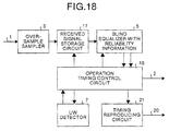
- Fig. 18 shows a structure of the receiver according to an eighth embodiment of the present invention.
- the same legends are provided to the components which are the same as those in the aforementioned third or fourth embodiments, and the description thereof is omitted.
- legend 20 denotes the reproduction timing output terminal
- legend 21 denotes the timing reproducing circuit.
- the operation which is the same as that in the fourth embodiment is performed basically, but a difference with the fourth embodiment is that, for example, the operation timing control circuit 18 creates timing information including finally selected timing and a UW detected result of the UW detector 7, and the timing reproducing circuit 21 outputs a reproduction timing signal based on the timing information to be a reference.
- an addition value of frequency deviation and parameters of the blind equalizer can be changed, and enlargement of frequency coverage where the receiver operates and a stable operation in a wider channel can be realized more accurately.
- the timing reproducing circuit 21 outputs a reproduction timing signal based on the timing information created by the operation timing control circuit 18 so that accuracy of timing synchronization can be heightened. For this reason, more satisfactory demodulation characteristic can be realized in comparison with the third or forth embodiments.
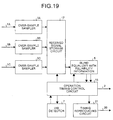
- Fig. 19 shows a structure of the receiver according to a ninth embodiment of the present invention.
- the same legends are provided to the components which are the same as those in the aforementioned firth to eight embodiments, and the description thereof is omitted.
- legends 1A, 1B and 2C denote received signal input terminals
- legends 3A, 3B and 3C denote over-sample samplers.
- an operation clock of the blind equalizer with reliability information 5 is set to be a larger value, and the operation timing control circuit 18 is set to be capable of processing a plurality of different received signals.
- an addition value of frequency deviation and parameters of the blind equalizer can be changed. Moreover, enlargement of frequency coverage where the receiver operates and a stable operation in a wider channel can be realized accurately.
- the timing reproducing circuit 21 outputs a reproduction timing signal based on timing information created by the operation timing control circuit 18 so that accuracy of timing synchronization can be heightened. For this reason, more satisfactory demodulation characteristic can be realized in comparison with the third or fourth embodiments.
- a plurality of the received signal input terminals and over-sample samplers are provided so that the one blind equalizer with reliability information 5 can process a plurality of different received signals.
- the receiver and the adaptive equalizer method of the present invention are useful for wireless communication such as mobile telephone, and particularly suitable for portable wireless communication equipments which are used in communication environments that inter-symbol interference occurs due to multipath propagation.
Landscapes
- Engineering & Computer Science (AREA)
- Computer Networks & Wireless Communication (AREA)
- Signal Processing (AREA)
- Power Engineering (AREA)
- Cable Transmission Systems, Equalization Of Radio And Reduction Of Echo (AREA)
- Synchronisation In Digital Transmission Systems (AREA)
- Digital Transmission Methods That Use Modulated Carrier Waves (AREA)
- Dc Digital Transmission (AREA)
Applications Claiming Priority (3)
| Application Number | Priority Date | Filing Date | Title |
|---|---|---|---|
| JP19314799 | 1999-07-07 | ||
| JP19314799 | 1999-07-07 | ||
| PCT/JP2000/003843 WO2001005056A1 (fr) | 1999-07-07 | 2000-06-14 | Recepteur et procede d'egalisation adaptative |
Publications (2)
| Publication Number | Publication Date |
|---|---|
| EP1115216A1 true EP1115216A1 (fr) | 2001-07-11 |
| EP1115216A4 EP1115216A4 (fr) | 2006-07-05 |
Family
ID=16303076
Family Applications (1)
| Application Number | Title | Priority Date | Filing Date |
|---|---|---|---|
| EP00939053A Withdrawn EP1115216A4 (fr) | 1999-07-07 | 2000-06-14 | Recepteur et procede d'egalisation adaptative |
Country Status (9)
| Country | Link |
|---|---|
| US (1) | US6560278B2 (fr) |
| EP (1) | EP1115216A4 (fr) |
| JP (1) | JP3506689B2 (fr) |
| KR (1) | KR100425893B1 (fr) |
| CN (1) | CN1210884C (fr) |
| AU (1) | AU751551B2 (fr) |
| CA (1) | CA2343153C (fr) |
| TW (1) | TW478260B (fr) |
| WO (1) | WO2001005056A1 (fr) |
Cited By (12)
| Publication number | Priority date | Publication date | Assignee | Title |
|---|---|---|---|---|
| EP1862776A2 (fr) | 2006-05-30 | 2007-12-05 | Fujitsu Limited | Système et procédé pour le découplage de multiples boucles de commande |
| EP1481519A4 (fr) * | 2002-03-04 | 2009-06-24 | Glowlink Communications Technology Inc | Detection et mesure des interferences contenues dans une porteuse numerique |
| US7760798B2 (en) | 2006-05-30 | 2010-07-20 | Fujitsu Limited | System and method for adjusting compensation applied to a signal |
| US7764757B2 (en) | 2006-05-30 | 2010-07-27 | Fujitsu Limited | System and method for the adjustment of offset compensation applied to a signal |
| US7787534B2 (en) | 2006-05-30 | 2010-08-31 | Fujitsu Limited | System and method for adjusting offset compensation applied to a signal |
| US7801208B2 (en) | 2006-05-30 | 2010-09-21 | Fujitsu Limited | System and method for adjusting compensation applied to a signal using filter patterns |
| US7804894B2 (en) | 2006-05-30 | 2010-09-28 | Fujitsu Limited | System and method for the adjustment of compensation applied to a signal using filter patterns |
| US7817712B2 (en) | 2006-05-30 | 2010-10-19 | Fujitsu Limited | System and method for independently adjusting multiple compensations applied to a signal |
| US7817757B2 (en) | 2006-05-30 | 2010-10-19 | Fujitsu Limited | System and method for independently adjusting multiple offset compensations applied to a signal |
| US7839955B2 (en) | 2006-05-30 | 2010-11-23 | Fujitsu Limited | System and method for the non-linear adjustment of compensation applied to a signal |
| US7839958B2 (en) | 2006-05-30 | 2010-11-23 | Fujitsu Limited | System and method for the adjustment of compensation applied to a signal |
| US7848470B2 (en) | 2006-05-30 | 2010-12-07 | Fujitsu Limited | System and method for asymmetrically adjusting compensation applied to a signal |
Families Citing this family (16)
| Publication number | Priority date | Publication date | Assignee | Title |
|---|---|---|---|---|
| US6907096B1 (en) * | 2000-09-29 | 2005-06-14 | Intel Corporation | Data recovery method and apparatus |
| US7010269B2 (en) * | 2001-05-07 | 2006-03-07 | Koninklijke Philips Electronics N.V. | Pre-equalizer structure based on PN511 sequence for terrestrial DTV reception |
| JP2002344362A (ja) * | 2001-05-14 | 2002-11-29 | Hitachi Kokusai Electric Inc | 等化装置、受信装置、及び等化方法並びに受信方法 |
| US7034297B2 (en) | 2003-03-05 | 2006-04-25 | Applied Materials, Israel, Ltd. | Method and system for use in the monitoring of samples with a charged particle beam |
| US7194025B2 (en) * | 2003-06-16 | 2007-03-20 | Harris Corporation | Updating adaptive equalizer coefficients using known or predictable bit patterns distributed among unknown data |
| CA2580547C (fr) * | 2004-09-24 | 2013-05-14 | Socovar S.E.C. | Procede et appareil d'egalisation multiple |
| US7397849B2 (en) * | 2005-03-18 | 2008-07-08 | Interdigital Technology Corporation | Channel estimation enhanced LMS equalizer |
| US7852912B2 (en) * | 2005-03-25 | 2010-12-14 | Agilent Technologies, Inc. | Direct determination equalizer system |
| FR2885434B1 (fr) * | 2005-05-09 | 2007-07-13 | Commissariat Energie Atomique | Procede d'estimation de la phase d'un mouvement d'un objet |
| WO2007088580A1 (fr) * | 2006-01-31 | 2007-08-09 | Mitsubishi Denki Kabushiki Kaisha | Procede de commande de communication, appareil de station de reception, appareil de station de transmission et systeme de communication |
| CN101083642B (zh) * | 2006-05-30 | 2010-10-20 | 富士通株式会社 | 用于调节施加给信号的偏移补偿的系统和方法 |
| US8441751B1 (en) * | 2006-08-18 | 2013-05-14 | Marvell International Ltd. | Dibit pulse extraction methods and systems |
| KR100757833B1 (ko) * | 2006-08-31 | 2007-09-11 | 삼성전자주식회사 | 디씨엠 디맵핑 장치 및 방법 |
| US7782934B2 (en) * | 2006-09-18 | 2010-08-24 | Silicon Image, Inc. | Parameter scanning for signal over-sampling |
| JP6273679B2 (ja) * | 2013-03-04 | 2018-02-07 | 株式会社リコー | 送受信システム、送受信方法及び受信装置 |
| CN104218990B (zh) * | 2014-09-30 | 2017-04-12 | 中国人民解放军信息工程大学 | 一种可见光通信系统及可见光通信方法 |
Family Cites Families (8)
| Publication number | Priority date | Publication date | Assignee | Title |
|---|---|---|---|---|
| JP2795935B2 (ja) | 1989-11-24 | 1998-09-10 | 三菱電機株式会社 | 最尤系列推定装置 |
| JPH03195129A (ja) | 1989-12-22 | 1991-08-26 | Mitsubishi Electric Corp | 最尤系列推定装置 |
| CA2037824C (fr) | 1990-03-20 | 1999-11-09 | Hiroshi Kubo | Circuit fonctionnant en diversite et circuit d'evaluation de la phase de trame (ou du temps d'echantillonnage) utilisant ce circuit |
| JP2623375B2 (ja) * | 1991-03-07 | 1997-06-25 | 松下電器産業株式会社 | データ受信装置 |
| JPH06216810A (ja) * | 1993-01-20 | 1994-08-05 | Fujitsu Ltd | 等化器の同期確立方式 |
| KR0134340B1 (ko) * | 1993-06-02 | 1998-04-27 | 김광호 | 블라인드 등화시스템의 알고리즘제어방법 |
| JP3102221B2 (ja) * | 1993-09-10 | 2000-10-23 | 三菱電機株式会社 | 適応等化器および適応ダイバーシチ等化器 |
| JP3125644B2 (ja) * | 1995-09-13 | 2001-01-22 | 松下電器産業株式会社 | 復調装置 |
-
2000
- 2000-06-14 KR KR10-2001-7002897A patent/KR100425893B1/ko not_active Expired - Fee Related
- 2000-06-14 JP JP2001509173A patent/JP3506689B2/ja not_active Expired - Fee Related
- 2000-06-14 WO PCT/JP2000/003843 patent/WO2001005056A1/fr not_active Ceased
- 2000-06-14 EP EP00939053A patent/EP1115216A4/fr not_active Withdrawn
- 2000-06-14 CN CNB008012504A patent/CN1210884C/zh not_active Expired - Fee Related
- 2000-06-14 AU AU54260/00A patent/AU751551B2/en not_active Ceased
- 2000-06-14 CA CA002343153A patent/CA2343153C/fr not_active Expired - Fee Related
- 2000-06-16 TW TW089111853A patent/TW478260B/zh not_active IP Right Cessation
-
2001
- 2001-02-27 US US09/793,774 patent/US6560278B2/en not_active Expired - Lifetime
Non-Patent Citations (2)
| Title |
|---|
| No further relevant documents disclosed * |
| See also references of WO0105056A1 * |
Cited By (15)
| Publication number | Priority date | Publication date | Assignee | Title |
|---|---|---|---|---|
| EP1481519A4 (fr) * | 2002-03-04 | 2009-06-24 | Glowlink Communications Technology Inc | Detection et mesure des interferences contenues dans une porteuse numerique |
| US7639761B2 (en) | 2002-03-04 | 2009-12-29 | Glowlink Communications Technology, Inc. | Detecting and measuring interference contained within a digital carrier |
| US7787534B2 (en) | 2006-05-30 | 2010-08-31 | Fujitsu Limited | System and method for adjusting offset compensation applied to a signal |
| EP1862776A3 (fr) * | 2006-05-30 | 2008-04-23 | Fujitsu Limited | Système et procédé pour le découplage de multiples boucles de commande |
| US7760798B2 (en) | 2006-05-30 | 2010-07-20 | Fujitsu Limited | System and method for adjusting compensation applied to a signal |
| US7764757B2 (en) | 2006-05-30 | 2010-07-27 | Fujitsu Limited | System and method for the adjustment of offset compensation applied to a signal |
| EP1862776A2 (fr) | 2006-05-30 | 2007-12-05 | Fujitsu Limited | Système et procédé pour le découplage de multiples boucles de commande |
| US7801208B2 (en) | 2006-05-30 | 2010-09-21 | Fujitsu Limited | System and method for adjusting compensation applied to a signal using filter patterns |
| US7804921B2 (en) | 2006-05-30 | 2010-09-28 | Fujitsu Limited | System and method for decoupling multiple control loops |
| US7804894B2 (en) | 2006-05-30 | 2010-09-28 | Fujitsu Limited | System and method for the adjustment of compensation applied to a signal using filter patterns |
| US7817712B2 (en) | 2006-05-30 | 2010-10-19 | Fujitsu Limited | System and method for independently adjusting multiple compensations applied to a signal |
| US7817757B2 (en) | 2006-05-30 | 2010-10-19 | Fujitsu Limited | System and method for independently adjusting multiple offset compensations applied to a signal |
| US7839955B2 (en) | 2006-05-30 | 2010-11-23 | Fujitsu Limited | System and method for the non-linear adjustment of compensation applied to a signal |
| US7839958B2 (en) | 2006-05-30 | 2010-11-23 | Fujitsu Limited | System and method for the adjustment of compensation applied to a signal |
| US7848470B2 (en) | 2006-05-30 | 2010-12-07 | Fujitsu Limited | System and method for asymmetrically adjusting compensation applied to a signal |
Also Published As
| Publication number | Publication date |
|---|---|
| CN1210884C (zh) | 2005-07-13 |
| CA2343153C (fr) | 2005-04-05 |
| JP3506689B2 (ja) | 2004-03-15 |
| EP1115216A4 (fr) | 2006-07-05 |
| US20010006533A1 (en) | 2001-07-05 |
| AU751551B2 (en) | 2002-08-22 |
| WO2001005056A1 (fr) | 2001-01-18 |
| TW478260B (en) | 2002-03-01 |
| KR100425893B1 (ko) | 2004-04-01 |
| US6560278B2 (en) | 2003-05-06 |
| CN1316136A (zh) | 2001-10-03 |
| AU5426000A (en) | 2001-01-30 |
| KR20010074971A (ko) | 2001-08-09 |
| CA2343153A1 (fr) | 2001-01-18 |
Similar Documents
| Publication | Publication Date | Title |
|---|---|---|
| US6560278B2 (en) | Receiver and an adaptive equalizer method | |
| JPWO2001005056A1 (ja) | 受信機および適応等化処理方法 | |
| Cozzo et al. | Joint channel estimation and data detection in space-time communications | |
| JP5248497B2 (ja) | ダイバーシティ信号の受信時にシンボル配列する方法及び装置 | |
| US6535554B1 (en) | PCS signal separation in a one dimensional channel | |
| US6898239B2 (en) | Method of detecting a sequence of information symbols, and a mobile station adapted to performing the method | |
| US7450924B1 (en) | Interference cancellation and receive diversity for single-valued modulation receivers | |
| EP1232617B1 (fr) | Procede et recepteur pour blanchissement de la perturbation d'un signal de communication | |
| US9160577B2 (en) | Hybrid SAIC receiver | |
| US7092438B2 (en) | Multilevel decision feedback equalizer | |
| US7010069B2 (en) | Method for co-channel interference identification and mitigation | |
| EP1456959B1 (fr) | Demodulation conjointe realisee a l'aide d'un egaliseur de viterbi possedant un nombre total adaptatif d'etats | |
| EP1481482B1 (fr) | Dispositifs et procedes de reception de signaux | |
| US6314148B1 (en) | Synchronization tracking method | |
| US7349493B2 (en) | Demodulation with separate branches for phase and amplitude | |
| WO2001045315A1 (fr) | Determination du temps d'echantillonnage de symboles d'un recepteur radio a decision ferme | |
| US6961391B2 (en) | Signal processor used for symbol recovery and methods therein | |
| GB2314488A (en) | MRC diversity circuit uses branch with maximum RSSI | |
| Jamal et al. | Adaptive MLSE performance on the D-AMPS 1900 channel | |
| EP1447926B1 (fr) | Recepteur a diversite spatiale, procede de commande de ce recepteur et programme associe | |
| JP3546833B2 (ja) | 無線受信装置及び高速等化処理方法 | |
| EP1475933B1 (fr) | Procédé de suppression d'interférence avec estimation itérative, semi-aveugle de canal | |
| JP3970478B2 (ja) | ビタビ等化器および送信データ系列判定方法 | |
| JPWO2006092830A1 (ja) | 受信装置 | |
| JP2005117126A (ja) | 復調回路 |
Legal Events
| Date | Code | Title | Description |
|---|---|---|---|
| PUAI | Public reference made under article 153(3) epc to a published international application that has entered the european phase |
Free format text: ORIGINAL CODE: 0009012 |
|
| 17P | Request for examination filed |
Effective date: 20010222 |
|
| AK | Designated contracting states |
Kind code of ref document: A1 Designated state(s): AT BE CH CY DE DK ES FI FR GB GR IE IT LI LU MC NL PT SE |
|
| RBV | Designated contracting states (corrected) |
Designated state(s): DE FR GB |
|
| RAP1 | Party data changed (applicant data changed or rights of an application transferred) |
Owner name: MITSUBISHI DENKI KABUSHIKI KAISHA |
|
| A4 | Supplementary search report drawn up and despatched |
Effective date: 20060607 |
|
| 17Q | First examination report despatched |
Effective date: 20061109 |
|
| STAA | Information on the status of an ep patent application or granted ep patent |
Free format text: STATUS: THE APPLICATION IS DEEMED TO BE WITHDRAWN |
|
| 18D | Application deemed to be withdrawn |
Effective date: 20081014 |