EP1119007A2 - Leitfähige Paste und Solarzelle damit - Google Patents
Leitfähige Paste und Solarzelle damit Download PDFInfo
- Publication number
- EP1119007A2 EP1119007A2 EP01100899A EP01100899A EP1119007A2 EP 1119007 A2 EP1119007 A2 EP 1119007A2 EP 01100899 A EP01100899 A EP 01100899A EP 01100899 A EP01100899 A EP 01100899A EP 1119007 A2 EP1119007 A2 EP 1119007A2
- Authority
- EP
- European Patent Office
- Prior art keywords
- surface electrode
- conductive paste
- solar cell
- aluminum powder
- layer
- Prior art date
- Legal status (The legal status is an assumption and is not a legal conclusion. Google has not performed a legal analysis and makes no representation as to the accuracy of the status listed.)
- Withdrawn
Links
Images

Classifications
-
- H—ELECTRICITY
- H01—ELECTRIC ELEMENTS
- H01B—CABLES; CONDUCTORS; INSULATORS; SELECTION OF MATERIALS FOR THEIR CONDUCTIVE, INSULATING OR DIELECTRIC PROPERTIES
- H01B1/00—Conductors or conductive bodies characterised by the conductive materials; Selection of materials as conductors
- H01B1/14—Conductive material dispersed in non-conductive inorganic material
- H01B1/16—Conductive material dispersed in non-conductive inorganic material the conductive material comprising metals or alloys
-
- H—ELECTRICITY
- H10—SEMICONDUCTOR DEVICES; ELECTRIC SOLID-STATE DEVICES NOT OTHERWISE PROVIDED FOR
- H10F—INORGANIC SEMICONDUCTOR DEVICES SENSITIVE TO INFRARED RADIATION, LIGHT, ELECTROMAGNETIC RADIATION OF SHORTER WAVELENGTH OR CORPUSCULAR RADIATION
- H10F77/00—Constructional details of devices covered by this subclass
- H10F77/20—Electrodes
- H10F77/206—Electrodes for devices having potential barriers
- H10F77/211—Electrodes for devices having potential barriers for photovoltaic cells
-
- Y—GENERAL TAGGING OF NEW TECHNOLOGICAL DEVELOPMENTS; GENERAL TAGGING OF CROSS-SECTIONAL TECHNOLOGIES SPANNING OVER SEVERAL SECTIONS OF THE IPC; TECHNICAL SUBJECTS COVERED BY FORMER USPC CROSS-REFERENCE ART COLLECTIONS [XRACs] AND DIGESTS
- Y02—TECHNOLOGIES OR APPLICATIONS FOR MITIGATION OR ADAPTATION AGAINST CLIMATE CHANGE
- Y02E—REDUCTION OF GREENHOUSE GAS [GHG] EMISSIONS, RELATED TO ENERGY GENERATION, TRANSMISSION OR DISTRIBUTION
- Y02E10/00—Energy generation through renewable energy sources
- Y02E10/50—Photovoltaic [PV] energy
Definitions
- the present invention relates to a conductive paste used for forming electrodes of ceramic electronic components, etc., and more particularly, the invention relates to a conductive paste which is suitable for use in forming back-surface electrodes of silicon solar cells, etc.
- a typical conductive paste conductive powder and glass frit are dispersed in an organic vehicle.
- a conductive paste containing aluminum powder as a principal ingredient is used in order to secure Ohmic contact with silicon substrates (Si wafers).
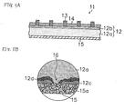
- a silicon solar cell 11 includes an Si wafer 12 consisting of a p-type silicon layer 12a and an n-type silicon layer 12b, a light-accepting-surface electrode 13 and an antireflection coating 14 formed on the light-accepting surface of the n-type silicon layer 12b, and a back-surface electrode 15 formed on the p-type silicon layer 12a.
- an electrode coating is formed by printing a conductive paste, in which aluminum powder 15a and glass frit are dispersed in an organic vehicle, on the side of the p-type silicon layer 12a of the Si wafer 12.
- the electrode coating is dried, and by firing at a temperature which is equal to or higher than the melting point of the aluminum powder, i.e., at 660°C or higher, with a near-infrared heating oven in air, the organic component is removed and the aluminum powder 15a is sintered, and thus the back-surface electrode 15 containing aluminum as a principal ingredient is obtained.
- the back-surface electrode 15 reacts with the p-type silicon layer 12a to form an Al-Si alloy layer 12c. Furthermore, Al ions diffuse into the p-type silicon layer 12a through the Al-Si alloy layer 12c from the back-surface electrode 15, and thus a p + electrolytic layer 12d is formed.
- the Al-Si alloy layer 12c and the p + electrolytic layer 12d secure Ohmic contact between the back-surface electrode 15 and the p-type silicon layer 12a and also improve the characteristics of the solar cell. For example, the reflection efficiency of long-wavelength light is improved, electrons are prevented from being recombined in the wafer, and the internal electric field is improved.
- aluminum powder is easily oxidized, and in the conductive paste described above, the surface of the aluminum powder is covered by an oxide layer.
- the oxide layer on the surface of aluminum powder is not particularly controlled, and particles of the aluminum powder have different degrees of oxidation in the surfaces thereof.
- the aluminum powder 15a covered by the oxide film has insufficient reactivity with silicon. Moreover, when firing is performed in air, since the thickness of the oxide film increases according to the diffusion law, the reactivity with silicon is further decreased. Additionally, since the surface of the Si wafer 12 has a texture structure composed of pyramidal irregularities on the order of several to 10 micrometers, a space occurs between the aluminum powder and the Si wafer 12, and the contact area between the aluminum powder 15a in the back-surface electrode 15 and the p-type silicon layer 12a, i.e., the area where the alloying reaction begins is reduced. Furthermore, the firing operation of the back-surface electrode 15 is completed in a short period of time, such as over several minutes, in order to inhibit the diffusion of impurities, such as glass components, which adversely affect the characteristics.
- the degree of oxidation of the aluminum powder depends on the thickness of the back-surface electrode 15 under the influence of the oxygen partial pressure in the vicinity of the interface between the back-surface electrode 15 and the p-type silicon layer 12a. That is, if the thickness of the back-surface electrode 15 is decreased, the oxygen partial pressure at the interface is increased and the reactivity of the back-surface electrode 15 is decreased, and thus the formation of the Al-Si alloy layer 12c and the p + electrolytic layer 12d is inhibited, resulting in the problems as described above.
- a conductive paste contains conductive powder and an organic vehicle.
- the conductive powder includes aluminum powder having an average particle diameter of 2 to 10 ⁇ m and having an oxide layer with a thickness of 2 to 10 nm on the surface thereof.
- a solar cell in another aspect of the present invention, includes a silicon substrate having a light-accepting surface, a light-accepting-surface electrode formed on the light-accepting surface of the silicon substrate, and a back-surface electrode formed of a conductive paste of the present invention on an opposite surface to the light-accepting surface of the silicon substrate.
- the aluminum powder which is used for a conductive paste of the present invention has an average particle diameter of 2 to 10 ⁇ m.
- the aluminum powder having an average particle diameter of 2 to 10 ⁇ m since the Al-Si contact area is increased regardless of the irregular structure of an Si wafer, a uniform alloy layer can be formed in the interface direction, and thus the coverage of the alloy layer can be increased.
- the average particle diameter of the aluminum powder is less than 2 ⁇ m, since the volumetric ratio of oxides in the aluminum powder is increased and the electrode resistivity increases, the wiring resistance of the silicon solar cell increases, resulting in degradation in the characteristics of the silicon solar cell, which is disadvantageous.
- the average particle diameter of the aluminum powder exceeds 10 ⁇ m, since the Al-Si contact area is not sufficiently secured, the coverage of the alloy layer is decreased.
- an oxide layer thereof has a thickness of 2 to 10 nm.
- the alloying reaction between Al and Si takes place at a high temperature of 600°C or more.
- the thickness of the oxide layer increases over time according to the parabolic rule. Therefore, in order to increase the coverage of the Al-Si alloy layer, the thickness of the oxide layer of the aluminum powder, which blocks the alloying reaction, is preferably set to be minimized in the initial state before heating.
- the thickness of the oxide layer is less than 2 nm, an excessive alloying reaction may cause the formation of Al-Si agglomerates or structural defects, such as cracking of the Si wafer.
- the thickness of the oxide layer exceeds 10 nm, for the reason described above, the Al-Si alloying reaction is not promoted.
- the conductive powder includes the aluminum powder in the amount of 80% by weight or more. More preferably, the conductive powder is nearly entirely composed of the aluminum powder. That is, in the conventional aluminum powder, the thickness and uniformity of the oxide layer are not controlled.
- the conductive paste contains the aluminum powder having an average particle diameter of 2 to 10 ⁇ m and having an oxide layer with a thickness of 2 to 10 nm on the surface thereof as a principal ingredient, and the thickness of the oxide layer of the aluminum powder is controlled. In a silicon solar cell provided with a back-surface electrode which is formed using such a conductive paste, a high conversion efficiency can be achieved.
- the content of the aluminum powder of the present invention in the total amount of aluminum powder constituting the conductive paste of the present invention is not specifically limited. That is, in response to the desired characteristics of the silicon solar cell, the thickness of the back-surface electrode, or material costs, it is possible to adjust the reactivity of the Al electrode by appropriately blending aluminum powders having different average particle diameters and having oxide layers with different thicknesses.
- organic vehicle contained in the conductive paste of the present invention an organic vehicle in which a cellulose-based resin, such as ethyl cellulose or nitrocellulose, an alkyd resin, or an acrylic resin is dissolved in a solvent, such as terpineol, Carbitol, or Cellosolve, may be used.
- a cellulose-based resin such as ethyl cellulose or nitrocellulose, an alkyd resin, or an acrylic resin is dissolved in a solvent, such as terpineol, Carbitol, or Cellosolve
- a solvent such as terpineol, Carbitol, or Cellosolve
- the conductive paste of the present invention may further contain glass frit.
- glass frit for example, PbO-B 2 O 3 -SiO 2 -based glass, or Bi 2 O 3 -B 2 O 3 -SiO 2 -based glass may be used.
- the glass frit is not limited thereto.
- FIGs. 1A and 1B A silicon solar cell in an embodiment of the present invention will be described with reference to FIGs. 1A and 1B.
- a silicon solar cell 1 includes an Si wafer 2 consisting of a p-type silicon layer 2a and an n-type silicon layer 2b, a light-accepting-surface electrode 3 and an antireflection coating 4 formed on the light-accepting surface of the Si wafer 2, and a back-surface electrode 5 formed on a surface opposite to the light-accepting surface.
- the light-accepting-surface electrode 3 and the antireflecting coating 4 are formed on the principal surface of the Si wafer 2 on the side of the n-type silicon layer 2b.
- a conductive film is formed on the principal surface of the Si wafer 2 on the side of the p-type silicon layer 2a using a conductive paste of the present invention, followed by firing.
- Al in the back-surface electrode 5 reacts with the p-type silicon layer 2a to form an Al-Si alloy layer 2c at the interface between the back-surface electrode 5 and the p-type silicon layer 2a on the side of the p-type silicon layer 2a, and Al ions diffuse into the p-type silicon layer 2 through the Al-Si alloy layer 2c to form a p + electrolytic layer 2d.
- the back-surface electrode 5 is formed using a conductive paste of the present invention which contains aluminum powder 5a having an average particle diameter of 2 to 10 ⁇ m and having an oxide layer with a thickness of 2 to 10 nm. Therefore, Al-Si agglomerates due to excessive alloying reaction are not produced, and regardless of the irregular structure of the Si wafer, the Al-Si contact area is increased, and thus the Al-Si alloy layer 2c and the p + electrolytic layer 2d having sufficient thicknesses are formed.
- the shapes of the light-accepting-surface electrode 3 and the antireflection coating 4 are not limited those described above in the embodiment.
- aluminum powders having the average particle diameter and the thickness of oxide layer as shown in Table 1 were prepared for Examples 1 to 9 and Comparative Examples 1 to 5. Additionally, the average particle diameters of the aluminum powders were measured by a laser diffraction-scattering-type particle size distribution tester, using a mixed solvent of ethanol and isopropyl alcohol as a disperse medium. The thickness of the oxide layer of the aluminum powder was determined by dividing the amount of oxide in the aluminum powder by the specific surface area thereof. The amount of oxide was measured by a method in which a predetermined amount of aluminum powder was heated in a carbon crucible to 2,000°C or more in air, and the amount of carbon dioxide generated was determined. The specific surface area was measured by the BET method.
- electrode coatings were formed by screen printing, on 350 ⁇ m thick Si wafers of predetermined sizes, using the conductive pastes in Examples 1 to 9 and Comparative Examples 1 to 5, followed by drying at 150°C. Firing was then performed in a near-infrared heating oven at a maximum temperature of 750°C to form back-surface electrodes, and thus test samples in Examples 1 to 9 and Comparative Examples 1 to 5 were obtained. In order to evaluate the characteristics, 3 types of test samples described below were produced.
- each sample for measuring resistivity a line electrode composed of a bent line with a width of 400 ⁇ m and an overall length of 200 mm was formed on an Si wafer with a size of 40 mm ⁇ 20 mm.
- the resistivity was obtained by measuring the electrical resistance between line electrodes and the thickness of the electrodes for each sample in Examples 1 to 9 and Comparative Examples 1 to 5, and the results thereof are summarized in Table 2.
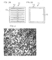
- each sample 11 for measuring conversion efficiency (Eff) As shown in FIG. 2A, an Si wafer 12 (14 mm by 14 mm square) consisting of a pn junction was prepared, and a light-accepting-surface electrode 13 composed of Ag was formed in a comb-like pattern on an n-type Si surface. A back-surface electrode 15 composed of Al was formed substantially entirely over a p-type Si surface.
- the conversion efficiency (Eff) was measured by a solar simulator (AM 1.5) at 25°C for each sample in Examples 1 to 9 and Comparative Examples 1 to 5, and the results thereof are summarized in Table 2.
- each sample for measuring the coverage of the Al-Si alloy layer and for evaluating structural defects, an Si wafer with a size of 40 mm ⁇ 20 mm consisting of a pn junction was prepared, and a back-surface electrode composed of Al was formed substantially entirely over a p-type Si surface so as to have a thickness of 50 ⁇ m.
- the appearance of the back-surface electrode after firing was observed to check the presence of agglomerates in the Al-Si alloy layer, protrusions, and cracking of the back-surface electrode.
- each sample in Examples 1 to 9 and Comparative Examples 1 to 5 was immersed in a 20% HCl aqueous solution to etch the back-surface electrode, and the state of the exposed Al-Si alloy layer was observed by an optical microscope.
- the coverage of the Al-Si alloy layer at the interface with the back-surface electrode was obtained by image analysis, and the results thereof are summarized in Table 2.
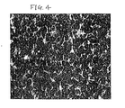
- Example 1 and Comparative Example 4 micrographs of exposed Al-Si alloy layers were taken, which are shown in FIGs. 3 and 4, respectively.
- the Al-Si alloy layers are shown by white regions and unreacted p-type silicon layers are shown as black spots. That is, as the amount of the black spots is decreased, the p-type silicon layer is much more covered by the Al-Si alloy layer.
- the electrode resistivity was in the range of 22 to 48 ⁇ cm, and the coverage of the Al-Si alloy layer was in the range of 65% to 95%, no structural defects were observed, and the conversion efficiency (Eff) was excellent in the range of 14.5% to 15.0%.
- the sample of Comparative Example 1 in which the aluminum powder had an average particle diameter of less than 2 ⁇ m, had a high electrode resistivity of 85 ⁇ cm, which was inferior, and also structural defects due to the occurrence of agglomerates were observed in some parts of the back-surface electrode.
- the conductive paste of the present invention in the silicon solar cell provided with the back-surface electrode, high conversion efficiency can be achieved, and also the thickness of the back-surface electrode and the thickness of the Si wafer can be decreased, and thus the size of the silicon solar cell can be reduced and the costs of the silicon solar cell can be reduced.
- the back-surface electrode is formed using the conductive paste of the present invention
- the silicon solar cell including the Si wafer consisting of the n-type silicon layer and the p-type silicon layer, the light-accepting-surface electrode and the antireflecting coating formed on the principal surface of the Si wafer on the side of the n-type silicon layer, and the back-surface electrode formed on the principal surface of the Si wafer on the side of the p-type silicon layer
- the back-surface electrode is formed by forming the electrode film on the principal surface of the Si wafer on the side of the p-type silicon layer using the conductive paste of the present invention, followed by firing, Al-Si agglomerates due to the excessive alloying reaction do not occur, and regardless of the irregular structure of the Si wafer, the Al-Si contact area can be increased, and the Al-Si alloy layer and p + electrolytic layer with sufficient thicknesses can be formed. Therefore, high conversion efficiency and low costs can be achieved.
Landscapes
- Chemical & Material Sciences (AREA)
- Dispersion Chemistry (AREA)
- Inorganic Chemistry (AREA)
- Photovoltaic Devices (AREA)
- Conductive Materials (AREA)
Applications Claiming Priority (2)
| Application Number | Priority Date | Filing Date | Title |
|---|---|---|---|
| JP2000012683 | 2000-01-21 | ||
| JP2000012683A JP2001202822A (ja) | 2000-01-21 | 2000-01-21 | 導電性ペースト |
Publications (2)
| Publication Number | Publication Date |
|---|---|
| EP1119007A2 true EP1119007A2 (de) | 2001-07-25 |
| EP1119007A3 EP1119007A3 (de) | 2002-09-25 |
Family
ID=18540370
Family Applications (1)
| Application Number | Title | Priority Date | Filing Date |
|---|---|---|---|
| EP01100899A Withdrawn EP1119007A3 (de) | 2000-01-21 | 2001-01-16 | Leitfähige Paste und Solarzelle damit |
Country Status (3)
| Country | Link |
|---|---|
| US (1) | US6558580B2 (de) |
| EP (1) | EP1119007A3 (de) |
| JP (1) | JP2001202822A (de) |
Cited By (4)
| Publication number | Priority date | Publication date | Assignee | Title |
|---|---|---|---|---|
| EP1575099A1 (de) * | 2004-03-09 | 2005-09-14 | RWE SCHOTT Solar GmbH | Verfahren zum Ausbilden einer Struktur |
| EP1691424A3 (de) * | 2005-02-09 | 2011-06-22 | centrotherm photovoltaics AG | Verfahren und Vorrichtung zur Herstellung von Siliziumsolarzellen |
| CN102646458A (zh) * | 2011-02-16 | 2012-08-22 | 中国钢铁股份有限公司 | 无铅导电胶及其制造方法 |
| US9385248B2 (en) | 2010-08-17 | 2016-07-05 | Lg Electronics Inc. | Solar cell panel |
Families Citing this family (22)
| Publication number | Priority date | Publication date | Assignee | Title |
|---|---|---|---|---|
| JP2003069055A (ja) * | 2001-06-13 | 2003-03-07 | Sharp Corp | 太陽電池セルとその製造方法 |
| JP3910072B2 (ja) * | 2002-01-30 | 2007-04-25 | 東洋アルミニウム株式会社 | ペースト組成物およびそれを用いた太陽電池 |
| US20040055635A1 (en) * | 2002-09-19 | 2004-03-25 | Hiroshi Nagakubo | Conductive paste, method for manufacturing solar battery, and solar battery |
| JP2004127987A (ja) * | 2002-09-30 | 2004-04-22 | Sharp Corp | 太陽電池セルおよびその製造方法 |
| JP3895254B2 (ja) * | 2002-10-07 | 2007-03-22 | シャープ株式会社 | 太陽電池セルの製造方法 |
| JP4668523B2 (ja) * | 2003-06-11 | 2011-04-13 | 東洋アルミニウム株式会社 | 太陽電池素子およびその製造方法 |
| WO2006011595A1 (ja) * | 2004-07-29 | 2006-02-02 | Kyocera Corporation | 太陽電池素子とその製造方法 |
| US7824579B2 (en) * | 2005-06-07 | 2010-11-02 | E. I. Du Pont De Nemours And Company | Aluminum thick film composition(s), electrode(s), semiconductor device(s) and methods of making thereof |
| JP2007019069A (ja) * | 2005-07-05 | 2007-01-25 | Toyo Aluminium Kk | ペースト組成物およびそれを用いた太陽電池素子 |
| JP4907333B2 (ja) * | 2006-12-26 | 2012-03-28 | 京セラ株式会社 | 太陽電池 |
| JP4970026B2 (ja) * | 2006-12-26 | 2012-07-04 | 京セラ株式会社 | 光電変換素子用導電性ペースト、光電変換素子、および光電変換素子の作製方法 |
| JP2008306023A (ja) * | 2007-06-08 | 2008-12-18 | Toyo Aluminium Kk | ペースト組成物と太陽電池素子 |
| JP2009146578A (ja) * | 2007-12-11 | 2009-07-02 | Noritake Co Ltd | 太陽電池および太陽電池用アルミニウムペースト |
| US20140335651A1 (en) * | 2008-11-14 | 2014-11-13 | Sichuan Yinhe Chemical Co., Ltd. | Inks and pastes for solar cell fabrication |
| JP5123830B2 (ja) * | 2008-11-26 | 2013-01-23 | ルネサスエレクトロニクス株式会社 | 反射防止膜、反射防止膜の製造方法、及び反射防止膜を用いた半導体装置 |
| CN101958361A (zh) * | 2009-07-13 | 2011-01-26 | 无锡尚德太阳能电力有限公司 | 透光薄膜太阳电池组件刻蚀方法 |
| CN102576776B (zh) * | 2009-07-22 | 2015-07-22 | 三菱电机株式会社 | 太阳能电池单元及其制造方法 |
| JP5649580B2 (ja) | 2009-09-18 | 2015-01-07 | 信越化学工業株式会社 | 太陽電池の製造方法 |
| TWI449189B (zh) * | 2011-02-10 | 2014-08-11 | 國立清華大學 | 一種用以提高破裂強度之太陽能基板 |
| WO2012111479A1 (ja) * | 2011-02-16 | 2012-08-23 | 株式会社 村田製作所 | 導電性ペースト、太陽電池、及び太陽電池の製造方法 |
| CN102651408A (zh) * | 2011-02-25 | 2012-08-29 | 叶哲良 | 一种用以提高破裂强度的太阳能基板 |
| WO2012148021A1 (ko) * | 2011-04-29 | 2012-11-01 | (주)창성 | 실리콘 태양전지의 저 휨 고특성 구현용 알루미늄 페이스트 조성물 |
Family Cites Families (1)
| Publication number | Priority date | Publication date | Assignee | Title |
|---|---|---|---|---|
| SU1415234A1 (ru) * | 1986-12-29 | 1988-08-07 | Предприятие П/Я Р-6668 | Проводникова паста |
-
2000
- 2000-01-21 JP JP2000012683A patent/JP2001202822A/ja active Pending
-
2001
- 2001-01-16 EP EP01100899A patent/EP1119007A3/de not_active Withdrawn
- 2001-01-22 US US09767217 patent/US6558580B2/en not_active Expired - Fee Related
Cited By (7)
| Publication number | Priority date | Publication date | Assignee | Title |
|---|---|---|---|---|
| EP1575099A1 (de) * | 2004-03-09 | 2005-09-14 | RWE SCHOTT Solar GmbH | Verfahren zum Ausbilden einer Struktur |
| WO2005088730A3 (de) * | 2004-03-09 | 2005-10-27 | Rwe Schott Solar Gmbh | Verfahren zum ausbilden einer struktur |
| EP1691424A3 (de) * | 2005-02-09 | 2011-06-22 | centrotherm photovoltaics AG | Verfahren und Vorrichtung zur Herstellung von Siliziumsolarzellen |
| US9385248B2 (en) | 2010-08-17 | 2016-07-05 | Lg Electronics Inc. | Solar cell panel |
| EP2421049B1 (de) * | 2010-08-17 | 2019-01-02 | LG Electronics Inc. | Solarzellenpaneel |
| CN102646458A (zh) * | 2011-02-16 | 2012-08-22 | 中国钢铁股份有限公司 | 无铅导电胶及其制造方法 |
| CN102646458B (zh) * | 2011-02-16 | 2014-02-12 | 中国钢铁股份有限公司 | 无铅导电胶及其制造方法 |
Also Published As
| Publication number | Publication date |
|---|---|
| EP1119007A3 (de) | 2002-09-25 |
| US6558580B2 (en) | 2003-05-06 |
| JP2001202822A (ja) | 2001-07-27 |
| US20010029977A1 (en) | 2001-10-18 |
Similar Documents
| Publication | Publication Date | Title |
|---|---|---|
| EP1119007A2 (de) | Leitfähige Paste und Solarzelle damit | |
| US7435361B2 (en) | Conductive compositions and processes for use in the manufacture of semiconductor devices | |
| US8168886B2 (en) | Paste for back contact-type solar cell | |
| JP6185232B2 (ja) | 低濃度ドーピングのエミッタを備えた半導体デバイスの製造における、鉛−テルルをベースとする酸化物を含有する導電性組成物の使用 | |
| EP2913311B1 (de) | Glas mit Wolfram und Blei in einer Solarzellenpaste | |
| EP2669899A1 (de) | Elektrisch leitfähige Pastenzusammensetzung mit niedrigem Metallgehalt | |
| JP2012502503A (ja) | 太陽電池電極 | |
| EP2355167A2 (de) | Verfahren zur herstellung von elektroden für solarzellen, substrat für in diesem verfahren hergestellte solarzellen sowie in diesem verfahren hergestellte solarzelle | |
| EP2696352B1 (de) | Silberpastenzusammensetzung zur formung einer elektrode und verfahren zu ihrer herstellung | |
| EP2490228A2 (de) | Silberpastenzusammensetzung und solarzelle damit | |
| TW201523896A (zh) | 結晶系矽太陽能電池及其製造方法 | |
| WO2010123967A2 (en) | Glass compositions used in conductors for photovoltaic cells | |
| EP2913139B1 (de) | Molybdän- und bleihaltiges Glas in einer Solarzellenpaste | |
| RU2690091C1 (ru) | Алюминиевая паста для изготовления тыльного контакта кремниевых солнечных элементов c тыльной диэлектрической пассивацией | |
| EP2474983A1 (de) | Elektrisch leitfähige paste, elektrode für ein halbleiterbauelement, halbleiterbauelement und verfahren zur herstellung des halbleiterbauelements | |
| EP2848657A1 (de) | Elektrisch leitende Paste mit haftungsförderndem Glas | |
| EP2824672B1 (de) | Elektrisch leitende Paste mit Ag-Teilchen mit einer multimodalen Durchmesserverteilung bei der Herstellung von Elektroden in MWT-Solarzellen | |
| Panek et al. | The new copper composite of pastes for Si solar cells front electrode application | |
| JP4714634B2 (ja) | 太陽電池電極用導電性ペースト | |
| Lossen et al. | Double printing nPERT cells with narrow contact layers | |
| KR101930284B1 (ko) | 태양전지 전극용 도전성 페이스트 및 이를 사용하여 제조된 태양전지 | |
| EP2896602B1 (de) | Silberarme, elektrisch leitende Paste | |
| WO2024101223A1 (ja) | 導電性ペースト、太陽電池及び太陽電池の製造方法 | |
| CN111630012A (zh) | 太阳能电池电极用导电性浆料以及包含于上述导电性浆料中的玻璃熔块、还有太阳能电池 | |
| EP2750139B1 (de) | Elektrisch leitende Paste mit einer vanadiumhaltigen Verbindung bei der Herstellung von Elektroden in MWT-Solarzellen |
Legal Events
| Date | Code | Title | Description |
|---|---|---|---|
| PUAI | Public reference made under article 153(3) epc to a published international application that has entered the european phase |
Free format text: ORIGINAL CODE: 0009012 |
|
| 17P | Request for examination filed |
Effective date: 20010116 |
|
| AK | Designated contracting states |
Kind code of ref document: A2 Designated state(s): AT BE CH CY DE DK ES FI FR GB GR IE IT LI LU MC NL PT SE TR |
|
| AX | Request for extension of the european patent |
Free format text: AL;LT;LV;MK;RO;SI |
|
| PUAL | Search report despatched |
Free format text: ORIGINAL CODE: 0009013 |
|
| RIC1 | Information provided on ipc code assigned before grant |
Free format text: 7H 01B 1/22 A, 7H 01L 31/00 B, 7H 01B 1/16 B |
|
| AK | Designated contracting states |
Kind code of ref document: A3 Designated state(s): AT BE CH CY DE DK ES FI FR GB GR IE IT LI LU MC NL PT SE TR |
|
| AX | Request for extension of the european patent |
Free format text: AL;LT;LV;MK;RO;SI |
|
| AKX | Designation fees paid |
Designated state(s): DE FR GB |
|
| GRAP | Despatch of communication of intention to grant a patent |
Free format text: ORIGINAL CODE: EPIDOSNIGR1 |
|
| STAA | Information on the status of an ep patent application or granted ep patent |
Free format text: STATUS: THE APPLICATION IS DEEMED TO BE WITHDRAWN |
|
| 18D | Application deemed to be withdrawn |
Effective date: 20040602 |