EP1119047A1 - Support plan pour un module à puce et methode de fabrication d'un module à puce - Google Patents
Support plan pour un module à puce et methode de fabrication d'un module à puce Download PDFInfo
- Publication number
- EP1119047A1 EP1119047A1 EP00100953A EP00100953A EP1119047A1 EP 1119047 A1 EP1119047 A1 EP 1119047A1 EP 00100953 A EP00100953 A EP 00100953A EP 00100953 A EP00100953 A EP 00100953A EP 1119047 A1 EP1119047 A1 EP 1119047A1
- Authority
- EP
- European Patent Office
- Prior art keywords
- flat carrier
- chip
- metallizations
- carrier
- metallization
- Prior art date
- Legal status (The legal status is an assumption and is not a legal conclusion. Google has not performed a legal analysis and makes no representation as to the accuracy of the status listed.)
- Withdrawn
Links
Images


Classifications
-
- H—ELECTRICITY
- H10—SEMICONDUCTOR DEVICES; ELECTRIC SOLID-STATE DEVICES NOT OTHERWISE PROVIDED FOR
- H10W—GENERIC PACKAGES, INTERCONNECTIONS, CONNECTORS OR OTHER CONSTRUCTIONAL DETAILS OF DEVICES COVERED BY CLASS H10
- H10W70/00—Package substrates; Interposers; Redistribution layers [RDL]
- H10W70/60—Insulating or insulated package substrates; Interposers; Redistribution layers
- H10W70/699—Insulating or insulated package substrates; Interposers; Redistribution layers for flat cards, e.g. credit cards
-
- G—PHYSICS
- G06—COMPUTING OR CALCULATING; COUNTING
- G06K—GRAPHICAL DATA READING; PRESENTATION OF DATA; RECORD CARRIERS; HANDLING RECORD CARRIERS
- G06K19/00—Record carriers for use with machines and with at least a part designed to carry digital markings
- G06K19/06—Record carriers for use with machines and with at least a part designed to carry digital markings characterised by the kind of the digital marking, e.g. shape, nature, code
- G06K19/067—Record carriers with conductive marks, printed circuits or semiconductor circuit elements, e.g. credit or identity cards also with resonating or responding marks without active components
- G06K19/07—Record carriers with conductive marks, printed circuits or semiconductor circuit elements, e.g. credit or identity cards also with resonating or responding marks without active components with integrated circuit chips
- G06K19/077—Constructional details, e.g. mounting of circuits in the carrier
- G06K19/07745—Mounting details of integrated circuit chips
-
- H—ELECTRICITY
- H10—SEMICONDUCTOR DEVICES; ELECTRIC SOLID-STATE DEVICES NOT OTHERWISE PROVIDED FOR
- H10W—GENERIC PACKAGES, INTERCONNECTIONS, CONNECTORS OR OTHER CONSTRUCTIONAL DETAILS OF DEVICES COVERED BY CLASS H10
- H10W72/00—Interconnections or connectors in packages
- H10W72/851—Dispositions of multiple connectors or interconnections
- H10W72/874—On different surfaces
- H10W72/884—Die-attach connectors and bond wires
-
- H—ELECTRICITY
- H10—SEMICONDUCTOR DEVICES; ELECTRIC SOLID-STATE DEVICES NOT OTHERWISE PROVIDED FOR
- H10W—GENERIC PACKAGES, INTERCONNECTIONS, CONNECTORS OR OTHER CONSTRUCTIONAL DETAILS OF DEVICES COVERED BY CLASS H10
- H10W90/00—Package configurations
- H10W90/701—Package configurations characterised by the relative positions of pads or connectors relative to package parts
- H10W90/721—Package configurations characterised by the relative positions of pads or connectors relative to package parts of bump connectors
- H10W90/724—Package configurations characterised by the relative positions of pads or connectors relative to package parts of bump connectors between a chip and a stacked insulating package substrate, interposer or RDL
-
- H—ELECTRICITY
- H10—SEMICONDUCTOR DEVICES; ELECTRIC SOLID-STATE DEVICES NOT OTHERWISE PROVIDED FOR
- H10W—GENERIC PACKAGES, INTERCONNECTIONS, CONNECTORS OR OTHER CONSTRUCTIONAL DETAILS OF DEVICES COVERED BY CLASS H10
- H10W90/00—Package configurations
- H10W90/701—Package configurations characterised by the relative positions of pads or connectors relative to package parts
- H10W90/751—Package configurations characterised by the relative positions of pads or connectors relative to package parts of bond wires
- H10W90/754—Package configurations characterised by the relative positions of pads or connectors relative to package parts of bond wires between a chip and a stacked insulating package substrate, interposer or RDL
Definitions
- the invention relates to a flat carrier, in particular for a chip module for use in chip cards, with one first and a second main page, where on the first Main a variety of first metallizations and on the second main page a corresponding number of second Metallization is provided.
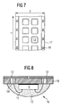
- Chip module for chip cards is shown in FIG. 8.
- the chip module 16 has a carrier 19, which is usually consists of epoxy resin.
- a semiconductor chip 9 is applied, for example is connected to the carrier 19 by means of adhesive.
- a metallization 13 is applied to the main side of the carrier 19.
- the metallization 13 forms the later accessible from the outside Contacts of the chip module 16.
- the metallization 13, which are usually made up of six or eight electrically there is separate contact areas, is over bond wires 11 with Contact pads of the semiconductor chip 9 connected.
- the bond wires 11 are through recesses 14 in the carrier 19 guided.
- a potting compound 15 applied, the semiconductor chip 9 and surrounds the bond wires 11.
- the chip module 16 shown in Figure 8 is in a so-called. "Reel-to-reel" process. With this procedure a clip carrier tape made of epoxy resin is provided which runs between two rolls as an endless belt.
- the carrier tape 17th is usually designed according to the JEDEC standard. This means that the carrier tape has a width of approximately 35 mm on.
- a section of such a carrier tape is shown in Figure 7.
- the carrier tape 17 points along its edges guide holes 18 with which the carrier tape 17 can be transported.
- the second Main page the metallization 13, e.g. a copper cladding, applied and then structured photolithographically as well as surface-finished (Ni An).
- the width y (35 mm) allows two metallizations 13 or later modules to be provided side by side and spaced apart on the carrier tape 17.
- module assembly process steps are on the first main page Semiconductor chips 9 applied. Then the contact pads of the semiconductor chips with the metallization 13 through the recesses connected together. Finally is poured with a potting compound. Finally be the completed chip modules 16, e.g. by sawing or Punching, isolated.
- the process steps just described are different Processing stations executed.
- the processing stations are located along the x-axis of the carrier tape 17.
- the carrier tape 17 is along the x direction to the passed individual processing stations, these can work in parallel.
- connection In the case of a carrier metallized on one side, the connection must be made between the semiconductor and the metallization by means of bond wires be made. Since the process step of bonding It brings temperatures of> 150 ° Celsius with it necessary, the material of the carrier is temperature resistant perform this step. The result conditional use of epoxy resin that has the required properties fulfilled, but has an impact on prices Unit cost of a chip module.
- a carrier that metallizes and plated through on both sides is to manufacture.
- Such a chip module is used in a chip card is, for example, from EP 0 071 311 A2 known.
- Figure 2 of this document is an integrated Module via its contact elements with the connection points connected by conductor tracks on a flexible Plastic film are applied.
- the plastic film is copper-clad on both sides, fully metallized and with corresponding contacts on the second main page the plastic film to the outside world.
- To increase the Strength of the integrated module on the plastic film is this made of an insulating and hardening plastic or encapsulating compound.
- a double-sided metallized carrier is rare in practice used, since this is used in a production with the described JEDEC standard compared to a one-sided metallized Carrier is disproportionately expensive.
- the object of the present invention is now to a manufacturing process for a chip module that is for use in a smart card is intended to provide that which in the known manufacturing processes from the prior art Technology mentioned disadvantages does not have.
- the one on SMD pick and place machine has adapted size.
- the cost of manufacturing a chip module can be significant can be reduced because of a standard SMD pick and place machine a much higher number of chip modules can be manufactured.
- a reel-to-reel process around 6000 chip modules can currently be manufactured.
- On SMD pick and place machine on the other hand, is able to handle approximately 50,000 To manufacture chip modules per hour. This is because that this process requires a significantly higher throughput enables.
- the manufacturing costs for a chip module can be lowered in that in a manufacturing facility required spatial dimensions for an SMD pick and place machine are much less than if by means a conventional reel-to-reel processing line of same throughput wanted to be achieved.
- the flat beam now makes it possible in an advantageous manner that not only two metallizations arranged side by side on the carrier can be, but depending on the dimensions of the flat carrier a significantly higher number of metallizations side by side can be arranged.
- the flat carrier advantageously consists of a thermoplastic or paper.
- significantly lower processing temperatures occur on. It is therefore possible to use a less expensive carrier material Use material.
- This can reduce the manufacturing costs of the chip module can be reduced.
- flip-chip contacting is advantageous, to reduce the overall height of the chip module. It can be this also the step of overmolding the semiconductor chip a sealing compound can be saved because the electrical connection between the semiconductor chip and the first metallization cannot be mechanically damaged.
- thermoplastic As plastic, e.g. ABS, PET, PVC or PC used become.
- the use of a thermoplastic also has the advantage that the connection of the Chip module with a chip card is particularly simple. This is because the chip card is made of a thermoplastic Plastic exists and thus the connection between the module and the chip card, for example by hot / cold gluing, Welding or an ultrasonic connection can be.
- a thermoplastic plastic has continue to have the advantage of being electrically insulating is. In this way, a short circuit between the first and the second metallization can be avoided.
- the second metallizations advantageously have second ones Contact areas provided for external contacting are.
- the second metallization is advantageous trained according to an ISO standard.
- a metallization can then have eight or six contact surfaces.
- the first metallizations advantageously have the first Contact surfaces that are arranged such that these when applying a semiconductor chip to the first main page of the flat carrier with contact surfaces of the semiconductor chip meet each other. This is no additional Rewiring necessary.
- the carrier takes on the task of Rewiring.
- the contact areas of the Semiconductor chips advantageously with a nickel-gold alloy Mistake. On the one hand, this makes the connection with the first contact surface is improved, the other one Corrosion of this electrical connection is prevented.
- the first Contact areas of the first metallization can be any be designed. They advantageously become particularly large executed so that the connection with the contact surfaces of the Semiconductor chips is easy to make.
- the second metallization can have second contact areas have, which for connection to a coil for contactless Data transmission are provided.
- the coil can be provided on a second, flat support.
- the invention also allows widely spaced To connect coil ends to the semiconductor chip, one two-sided metallization with a via is not on the flat carrier on which the coil is applied, must be made. Rather, the through-connection takes place in the flat chip module carrier according to the invention, whereby the manufacturing cost of a contactless smart card can be drastically reduced.
- the first and the second metallizations arranged in a grid and through Separation areas spaced apart.
- the grid-like arrangement the metallization enables quick work of an SMD pick and place machine based on the collect and place process Semiconductor chips on respective first metallizations can muster.
- the flat carrier advantageously has a size of 368 x 460 mm. This size corresponds to the current standard Dimensions processed with standard SMD pick and place machines can be. On such a flat surface Carriers can, depending on the design, approx. 700 ISO standard chip modules, each of which has eight contact surfaces, be provided. Alternatively, it would also be conceivable instead of this Formats to use continuous sheets or other formats.
- the grid-like arrangement of the metallizations corresponding to the area of a chip module enables a special simple, inexpensive and environmentally friendly production.
- the flat carrier becomes fully coated with copper. Then this Layer photomasked and etched. Because of the flat arrangement of the metallizations only a few non-metallized areas remain, only a little copper has to be etched away and into the wastewater be rinsed. After copper metallization, then finishing in the usual way.
- the manufacturing process for a chip module which is the starting product a flat carrier with a variety of has corresponding metallizations, each later Are part of a chip module, is therefore particularly simple, since the coil production for a contactless chip card Known use of plastic sheets with etched coil are. On these plastic sheets, the antenna carrier is used as Stamped out inlay. The plastic arch is then fully laminated with copper and then structured. The manufacturing process known from antenna production can remain unchanged for the manufacture of the two-sided metallized carrier can be used. Because the "Packing density" of the metallizations on the flat carrier However, it is very high, so that only little useless Remaining space is a huge savings in terms of Manufacturing costs possible.
- the semiconductor chips through an SMD pick and place machine on the flat Carrier applied. Because SMD pick and place machines versus one Manufacturing process according to the reel-to-reel process essential Working faster can be essential at the same time more chip modules are manufactured.
- the contact areas of the semiconductor chip are advantageously already in the wafer composite with a nickel-gold alloy chemically treated.
- the separation of the Chip modules made by cutting or punching.
- Every first and every second Metallization is electrical with one another via vias connected.
- the first metallization is designed that the contact surfaces with the contact surfaces of a Semiconductor chips directly, i.e. without bond wires, with each other can be connected.
- FIG. 2 shows a top view of the second main page a carrier separated from the flat carrier.
- the second main page 3 includes the second metallization, the has eight second contact surfaces 7 in the present example.
- the eight contact surfaces 7 are in accordance with the ISO standard arranged and electrically separated from each other.
- FIG. 3 shows a top view of the first main page, i.e. the back of Figure 2.
- the first metallization 4 has first contact surfaces 6, which with contact surfaces of a semiconductor chip.
- Via ladder tracks 21 is each first contact surface 6 with a via 8 connected to an electrical contact associated second contact surface 7 from Figure 2.
- the carrier thus takes over one for the semiconductor chip Rewiring.
- the electrical connection of the first and The second contact surfaces 6, 7 can be of different types respectively.
- the via could also take place according to the so-called "blackhole” method. Here carbon is deposited in the punched holes and then deposited copper.
- FIG. 4 shows a cross section of a chip module 26 that produced on a flat carrier 1 according to the invention has been.
- the spatial arrangement of the first and the second contact surfaces 6.7 to one another clearly.
- a semiconductor chip 9, which has contact surfaces 10, is with these connected to the first contact surfaces 6.
- the between the the first main side 2 and the space formed by the semiconductor chip can be filled in with an "underfiller".
- FIG. 5 shows a top view of the second main side 3 of a Chip module 26, in the metallizations for contacting are designed with a coil.
- two opposing second contact surfaces 7 are provided on the second main page 3 . These are each via vias 8 and Conductor tracks 21 with first contact surfaces 6 (dashed lines shown) connected.
- the first contact surfaces 6 serve to make an electrical contact to a semiconductor chip 9 (shown in dashed lines) to produce the first Main page 2 is applied.
- Figure 7 shows a cross section through a carrier layer 25 on which a Coil 22 is applied.
- the coil 22 can for example etched or fully laminated with copper and then structured or using a conductive paste and subsequent germination applied to the carrier layer 25 have been.
- the coil 22 three coil turns 24.
- the coil connections 23 come in the present figure on the left side of the support layer 25 to lie on.
- the flat carrier 1 is advantageously made of a thermoplastic Made of plastic. However, it is also the one Conceivable use of paper on which the structured metallizations applied using additive technology or laminating technology become.
- the total thickness of the module depends on the materials used.
- One from a thermoplastic Plastic sheet carrier usually has a thickness of 150 to 200 ⁇ m, the connection technology is already included in the metallization.
- the fat a semiconductor chip is usually between 120 and 185 ⁇ m. So when using standard materials Module thicknesses of 270 to 385 ⁇ m can already be achieved.
- the fat of the chip modules used in the prior art, as it is in Figure 8 is described, if a potting compound is provided around the semiconductor chip approx. 500 ⁇ m. Becomes a UV cover provided, the thickness is approx. 580 ⁇ m.
- the use of the Flat carrier according to the invention enables in addition to extraordinary high cost savings also in production particularly thin chip modules. These have the advantage that they can withstand mechanical bending stresses such as occur in daily use with
- the cost of manufacturing a chip module is essentially are determined by the carrier tape costs (do this about 60% of the material cost) is the use of a common thermoplastic material as flat Carrier for the chip modules compared to an epoxy resin Carrier tape advantageous to a large cost reduction to achieve.
Landscapes
- Engineering & Computer Science (AREA)
- Computer Hardware Design (AREA)
- Microelectronics & Electronic Packaging (AREA)
- Physics & Mathematics (AREA)
- General Physics & Mathematics (AREA)
- Theoretical Computer Science (AREA)
- Credit Cards Or The Like (AREA)
Priority Applications (2)
| Application Number | Priority Date | Filing Date | Title |
|---|---|---|---|
| EP00100953A EP1119047A1 (fr) | 2000-01-18 | 2000-01-18 | Support plan pour un module à puce et methode de fabrication d'un module à puce |
| PCT/DE2001/000156 WO2001054193A2 (fr) | 2000-01-18 | 2001-01-16 | Support plan pour un module de puce, et procede de fabrication de ce module |
Applications Claiming Priority (1)
| Application Number | Priority Date | Filing Date | Title |
|---|---|---|---|
| EP00100953A EP1119047A1 (fr) | 2000-01-18 | 2000-01-18 | Support plan pour un module à puce et methode de fabrication d'un module à puce |
Publications (1)
| Publication Number | Publication Date |
|---|---|
| EP1119047A1 true EP1119047A1 (fr) | 2001-07-25 |
Family
ID=8167653
Family Applications (1)
| Application Number | Title | Priority Date | Filing Date |
|---|---|---|---|
| EP00100953A Withdrawn EP1119047A1 (fr) | 2000-01-18 | 2000-01-18 | Support plan pour un module à puce et methode de fabrication d'un module à puce |
Country Status (2)
| Country | Link |
|---|---|
| EP (1) | EP1119047A1 (fr) |
| WO (1) | WO2001054193A2 (fr) |
Cited By (1)
| Publication number | Priority date | Publication date | Assignee | Title |
|---|---|---|---|---|
| EP1498842A4 (fr) * | 2002-04-01 | 2006-02-15 | Ubique Id Corp K | Dispositif de communication et son boitier |
Families Citing this family (1)
| Publication number | Priority date | Publication date | Assignee | Title |
|---|---|---|---|---|
| WO2013023326A1 (fr) * | 2011-08-18 | 2013-02-21 | 上海长丰智能卡有限公司 | Bande support pour un module novateur de carte intelligente, module de carte intelligente, procédé de production du module et carte intelligente |
Citations (5)
| Publication number | Priority date | Publication date | Assignee | Title |
|---|---|---|---|---|
| DE9303877U1 (de) * | 1993-03-18 | 1993-05-19 | Schulten, Thomas, 4600 Dortmund | Adapterkarte für D-Netz Autotelefone |
| US5255430A (en) * | 1992-10-08 | 1993-10-26 | Atmel Corporation | Method of assembling a module for a smart card |
| EP0599194A1 (fr) * | 1992-11-27 | 1994-06-01 | Esec Sempac S.A. | Module électronique ultramince |
| WO1997044823A1 (fr) * | 1996-05-17 | 1997-11-27 | Siemens Aktiengesellschaft | Substrat pour puce de semiconducteur |
| DE19709985A1 (de) * | 1997-03-11 | 1998-09-17 | Pav Card Gmbh | Chipkarte, Verbindungsanordnung und Verfahren zum Herstellen einer Chipkarte |
-
2000
- 2000-01-18 EP EP00100953A patent/EP1119047A1/fr not_active Withdrawn
-
2001
- 2001-01-16 WO PCT/DE2001/000156 patent/WO2001054193A2/fr not_active Ceased
Patent Citations (5)
| Publication number | Priority date | Publication date | Assignee | Title |
|---|---|---|---|---|
| US5255430A (en) * | 1992-10-08 | 1993-10-26 | Atmel Corporation | Method of assembling a module for a smart card |
| EP0599194A1 (fr) * | 1992-11-27 | 1994-06-01 | Esec Sempac S.A. | Module électronique ultramince |
| DE9303877U1 (de) * | 1993-03-18 | 1993-05-19 | Schulten, Thomas, 4600 Dortmund | Adapterkarte für D-Netz Autotelefone |
| WO1997044823A1 (fr) * | 1996-05-17 | 1997-11-27 | Siemens Aktiengesellschaft | Substrat pour puce de semiconducteur |
| DE19709985A1 (de) * | 1997-03-11 | 1998-09-17 | Pav Card Gmbh | Chipkarte, Verbindungsanordnung und Verfahren zum Herstellen einer Chipkarte |
Cited By (1)
| Publication number | Priority date | Publication date | Assignee | Title |
|---|---|---|---|---|
| EP1498842A4 (fr) * | 2002-04-01 | 2006-02-15 | Ubique Id Corp K | Dispositif de communication et son boitier |
Also Published As
| Publication number | Publication date |
|---|---|
| WO2001054193A3 (fr) | 2002-02-14 |
| WO2001054193A2 (fr) | 2001-07-26 |
Similar Documents
| Publication | Publication Date | Title |
|---|---|---|
| DE69716310T2 (de) | Chipkarte und chipkartenmodul | |
| DE69706280T2 (de) | Kontaktloses elektronisches modul für karte oder etikette | |
| EP0919041B1 (fr) | Procede de fabrication d'un module de carte a puce pour carte a puce combinee | |
| EP0869453B1 (fr) | Procédé de fabrication de carte à puce | |
| EP1271399B1 (fr) | Porteur de données avec circuit intégré | |
| DE69531845T2 (de) | Herstellungsverfahren einer Kombi-Karte | |
| DE19500925A1 (de) | Chipkarte zur kontaktlosen Datenübertragung | |
| EP0891603B1 (fr) | Substrat non conducteur formant une bande ou un flanc, sur lequel sont formes une pluralite d'elements porteurs | |
| EP0992939A1 (fr) | Méthode de fabrication d'un microtransponder | |
| DE19651566A1 (de) | Chip-Modul sowie Verfahren zu dessen Herstellung | |
| WO2010034820A1 (fr) | Antenne pour balise rfid | |
| EP0780004A1 (fr) | Circuit avec module sous forme de carte a puce connecte a une bobine | |
| DE69805404T2 (de) | Verfahren zum herstellen kontaktloser karten mit antennenverbindung durch gelötete drähte | |
| EP1428260B1 (fr) | Substrat non conducteur formant une bande ou un flan, sur lequel est formee une pluralite d'elements de support | |
| EP1388121B1 (fr) | Procede et demi-produit destines a la fabrication d'une carte a puce comportant une bobine | |
| DE602004004647T2 (de) | Verfahren zum zusammenbauen eines elektronischen komponent auf einem substrat | |
| DE69718223T2 (de) | Massenspeicher und Herstellungsverfahren dafür | |
| DE102021005830A1 (de) | Kartenförmiger Datenträger und Verfahren zum Herstellen eines kartenförmigen Datenträgers | |
| WO2008138531A1 (fr) | Système de transmission sans contact et procédé de réalisation associé | |
| EP1119047A1 (fr) | Support plan pour un module à puce et methode de fabrication d'un module à puce | |
| EP4315161B1 (fr) | Carte à puce et procédé de fabrication d'une carte à puce | |
| DE10236666A1 (de) | Verfahren zum Herstellen von Kontaktlosen und/oder gemischten Chipkarten | |
| DE102008039445B4 (de) | Zwischenprodukt für ein kartenförmiges Raumgebilde zur Ausbildung eines Transponders und Verfahren zur Herstellung desselben | |
| DE19844089C2 (de) | Verfahren zur Herstellung von Transponderanordnungen | |
| DE19609149A1 (de) | Chipkarte |
Legal Events
| Date | Code | Title | Description |
|---|---|---|---|
| PUAI | Public reference made under article 153(3) epc to a published international application that has entered the european phase |
Free format text: ORIGINAL CODE: 0009012 |
|
| AK | Designated contracting states |
Kind code of ref document: A1 Designated state(s): AT BE CH CY DE DK ES FI FR GB GR IE IT LI LU MC NL PT SE |
|
| AX | Request for extension of the european patent |
Free format text: AL;LT;LV;MK;RO;SI |
|
| 17P | Request for examination filed |
Effective date: 20020118 |
|
| AKX | Designation fees paid |
Free format text: AT BE CH CY DE DK ES FI FR GB GR IE IT LI LU MC NL PT SE |
|
| STAA | Information on the status of an ep patent application or granted ep patent |
Free format text: STATUS: THE APPLICATION HAS BEEN WITHDRAWN |
|
| 18W | Application withdrawn |
Withdrawal date: 20020531 |