EP1120660A2 - Vorrichtung und Verfahren zur Auswertung von offsetspannungsbehafteten digitalen Signalen - Google Patents
Vorrichtung und Verfahren zur Auswertung von offsetspannungsbehafteten digitalen Signalen Download PDFInfo
- Publication number
- EP1120660A2 EP1120660A2 EP01100375A EP01100375A EP1120660A2 EP 1120660 A2 EP1120660 A2 EP 1120660A2 EP 01100375 A EP01100375 A EP 01100375A EP 01100375 A EP01100375 A EP 01100375A EP 1120660 A2 EP1120660 A2 EP 1120660A2
- Authority
- EP
- European Patent Office
- Prior art keywords
- threshold value
- signal
- comparator
- output
- input
- Prior art date
- Legal status (The legal status is an assumption and is not a legal conclusion. Google has not performed a legal analysis and makes no representation as to the accuracy of the status listed.)
- Granted
Links
Images

Classifications
-
- H—ELECTRICITY
- H04—ELECTRIC COMMUNICATION TECHNIQUE
- H04L—TRANSMISSION OF DIGITAL INFORMATION, e.g. TELEGRAPHIC COMMUNICATION
- H04L25/00—Baseband systems
- H04L25/02—Details ; arrangements for supplying electrical power along data transmission lines
- H04L25/06—DC level restoring means; Bias distortion correction ; Decision circuits providing symbol by symbol detection
- H04L25/061—DC level restoring means; Bias distortion correction ; Decision circuits providing symbol by symbol detection providing hard decisions only; arrangements for tracking or suppressing unwanted low frequency components, e.g. removal of DC offset
-
- G—PHYSICS
- G01—MEASURING; TESTING
- G01R—MEASURING ELECTRIC VARIABLES; MEASURING MAGNETIC VARIABLES
- G01R31/00—Arrangements for testing electric properties; Arrangements for locating electric faults; Arrangements for electrical testing characterised by what is being tested not provided for elsewhere
- G01R31/28—Testing of electronic circuits, e.g. by signal tracer
- G01R31/30—Marginal testing, e.g. by varying supply voltage
- G01R31/3004—Current or voltage test
-
- G—PHYSICS
- G01—MEASURING; TESTING
- G01R—MEASURING ELECTRIC VARIABLES; MEASURING MAGNETIC VARIABLES
- G01R31/00—Arrangements for testing electric properties; Arrangements for locating electric faults; Arrangements for electrical testing characterised by what is being tested not provided for elsewhere
- G01R31/28—Testing of electronic circuits, e.g. by signal tracer
- G01R31/317—Testing of digital circuits
- G01R31/3181—Functional testing
- G01R31/319—Tester hardware, i.e. output processing circuits
- G01R31/3193—Tester hardware, i.e. output processing circuits with comparison between actual response and known fault free response
Definitions
- the invention relates to an apparatus and a method for Evaluation of digital signals with offset voltage.
- An evaluation of digital signals with offset voltage is caused by an undesired change in the offset voltage difficult during operation.
- Such undesirable Changes in the offset voltage can, for example due to temperature influences and an aging of Components in the signal path of the digital signal are caused.
- the invention is based on this prior art the task is to show a way like the one above Disadvantages described known devices avoided can be.
- Claim 13 relates to a method for the evaluation of digital signals with offset voltage.
- the advantages of the invention are in particular that by automatically adjusting the response threshold of the Comparator of the evaluation circuit to the present one Offset voltage the influence of the offset voltage on the evaluation digital signals with offset voltage are eliminated becomes.
- the invention is independent of the signal coding of the digital signals received. It also allows one Evaluation of high-frequency digital signal sequences with not DC-free coding, for example NRZ coding. Further advantages of the invention are the reduction the influence of external interference signals on the evaluation circuit. Because in the claimed level-sensitive evaluation the output signal is not saved Interference signals are only output as long as they are on the Act circuit.
- the digital signals fed to an evaluation circuit can be applied with an offset voltage during operation subject to unwanted changes. These changes can affect the temperature and aging of components, which are in the signal path of the digital signal his.
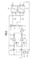
- An embodiment of such Digital signal with offset voltage is shown in FIG. 1 shown.
- the digital signal shown, which with any Coding is provided, has HIGH level H and LOW level L, each of which is overlaid by an offset voltage O. are.
- Such a digital signal with offset voltage becomes the input 1 of the device shown in FIG fed.
- the input 1 of the device shown is with the input a switch 2 connected. This is also the case at input 1 applied input signal to the input 12 of a second comparator 14 and the input 13 of a first comparator 15.
- the output of switch 2 is connected via a resistor 3 a first connection of a capacitor serving as a memory 4 and connected to the input of an amplifier 5.
- the second connection of the capacitor 4 is at a reference potential, for example mass.
- the base 6 one Circuit for setting a first threshold value SU and a second threshold SO.
- This circuit points a constant current source 9 and one between the constant current source and the base point 6 arranged in series from two ohmic resistors 7 and 8.
- the second threshold SO At the connection point between the constant current source 9 and the resistor 8 there is the second threshold SO. This becomes an entrance 11 of the second comparator 14 supplied.
- the first threshold SU tapped, which is the input 10 of the first comparator 15 is forwarded.
- the second threshold is greater than the first threshold.
- the second comparator 14 compares the second Threshold value SO with the offset voltage present at input 1 digital signal. The latter is smaller than the second threshold, then the output 16 of the first Comparator 14 provided a message signal. This contains information that the level of the transmitted digital signal due to aging effects of components in the signal path has dropped so much that maintenance of the device or replacement of components is necessary is.
- the first comparator 15 compares the first Threshold value SU with the offset voltage present at input 1 digital signal. The latter is smaller than the first threshold, then the output 17 of the first Comparator 15 an offset voltage-free LOW level signal made available. However, it is larger than that first threshold, then at the output 17 of the first comparator 15 an offset voltage-free HIGH level signal for Provided.
- the first comparator 15 has a further output 18. This is always when at the output 17 of the first comparator 15 there is an offset voltage-free LOW level signal, issued a control signal for the switch 2, which turns on switch 2, i.e. in the permeable Condition.
- the threshold values for the comparators 14 and 15 each time a LOW level signal is present in the offset voltage digital input signal sequence to the currently existing offset voltage adjusted. This allows one level-sensitive evaluation of the received digital signal without using a capacitor coupling and without bushing a differentiation of the input signal.
- FIG. 3 shows a second exemplary embodiment of a device for the evaluation of offset voltage digital Signals. This device differs from that in the device shown in Figure 2 essentially by that they are parallel to the signal path with switch 2, the Resistor 3, capacitor 4, amplifier 26 and one Resistor 27 another signal path with a switch 19, a resistor 20, a memory 21, an amplifier 22 and a resistor 23.
- This additional circuit is signal distortion to reduce that in the device according to FIG. 2 when there are signals with slowly rising edges may occur.
- the time constants of the RC elements are 20/21 or 3/4 selected differently.
- the RC link 3/4 has one large time constant of 1 ms.
- the RC link 20/21 has one small time constant of 1 ns.
- the analog amplifiers 22, 26 and 5 is make sure that the offset voltage of the amplifier is small compared to the minimum value of the digital signal to be recorded is.
- the amplifiers 22 and 5 must be fast amplifiers and the comparators 14 and 15 as fast comparators can be realized since the voltage across the capacitor 21st reach the HIGH level of the signal for the duration of a bit got to.
- the signal transit time must be taken into account and the duty cycle of switches 2 and 19 the leakage currents (offset and bias currents) are also taken into account become. These may contact the capacitors 4 and 21 Tension and also that at the connection point between the Resistors 23 and 27 do not affect the applied voltage.
Landscapes
- Engineering & Computer Science (AREA)
- General Engineering & Computer Science (AREA)
- Physics & Mathematics (AREA)
- General Physics & Mathematics (AREA)
- Power Engineering (AREA)
- Computer Networks & Wireless Communication (AREA)
- Signal Processing (AREA)
- Measurement Of Current Or Voltage (AREA)
- Manipulation Of Pulses (AREA)
- Analogue/Digital Conversion (AREA)
- Tests Of Electronic Circuits (AREA)
- Dc Digital Transmission (AREA)
Abstract
Description
- FIG 1
- ein Ausführungsbeispiel für ein offsetspannungsbehaftetes digitales Signal,
- FIG 2
- ein Schaltbild einer ersten Vorrichtung zur Auswertung von digitalen Signalen und
- FIG 3
- ein Schaltbild einer zweiten Vorrichutng zur Auswertung von digitalen Signalen.
Claims (13)
- Vorrichtung zur Auswertung von digitalen Signalen, mit einem Signaleingang (1),einem mit dem Signaleingang über einen Schalter (2) verbundenen Speicher (4),Mitteln (7, 8, 9) zur Einstellung eines ersten Schwellenwertes (SU) undeinem ersten Komparator (15) zum Vergleichen des Eingangssignals mit dem ersten Schwellenwert, um beim Vorliegen eines Eingangssignals, welches größer ist als der erste Schwellenwert, ausgangsseitig ein HIGH-Pegel-Signal und beim Vorliegen eines Eingangssignals, welches kleiner ist als der erste Schwellenwert, ausgangsseitig ein LOW-Pegel-Signal zur Verfügung zu stellen, wobeider erste Komparator (15) einen Ausgang (18) aufweist, an welchem beim Vorliegen eines Eingangssignals, welches kleiner ist als der erste Schwellenwert, ein den Schalter (2) schließendes Steuersignal bereitgestellt wird, und wobei der Speicher (4) mit einem Fußpunkt (6) der Mittel (7, 8, 9) zur Einstellung des Schwellenwertes verbunden ist.
- Vorrichtung nach Anspruch 1, dadurch gekennzeichnet, dass sie einen zweiten Komparator (14) enthält, welcher einen ersten Eingang (11) für einen zweiten Schwellenwert (SO), der größer ist als der erste Schwellenwert, einen mit dem Signaleingang (1) verbundenen zweiten Eingang (12) und einen Ausgang (16) aufweist, an welchem beim Vorliegen eines Eingangssignals, welches kleiner ist als der zweite Schwellenwert, ein Meldesignal ausgegeben wird.
- Vorrichtung nach Anspruch 1 oder 2, dadurch gekennzeichnet, dass der Ausgang (18), an dem das Steuersignal für den Schalter (2) anliegt, ein weiterer Ausgang des ersten Komparators (15) ist.
- Vorrichtung nach einem der vorhergehenden Ansprüche, dadurch gekennzeichnet, dass die Mittel zur Einstellung der Schwellenwerte eine Konstantstromquelle (9) und eine mit der Konstantstromquelle verbundene Reihenschaltung aus zwei Widerständen (7, 8) enthalten.
- Vorrichtung nach Anspruch 4, dadurch gekennzeichnet, dass der zweite Schwellenwert zwischen der Konstantstromquelle (9) und dem mit der Konstantstromquelle verbundenen ersten Widerstand (8) der Reihenschaltung abgreifbar ist.
- Vorrichtung nach Anspruch 5, dadurch gekennzeichnet, dass der erste Schwellenwert zwischen den beiden Widerständen (7, 8) der Reihenschaltung abgreifbar ist.
- Vorrichtung nach einem der vorhergehenden Ansprüche, dadurch gekennzeichnet, dass der von der Konstantstromquelle (9) abgelegene Anschluß der Reihenschaltung der Widerstände (7, 8) der Fußpunkt (6) ist.
- Vorrichtung nach einem der vorhergehenden Ansprüche, dadurch gekennzeichnet, dass der Fußpunkt (6) mit dem Speicher (4) über einen Verstärker (5) verbunden ist.
- Vorrichtung nach einem der vorhergehenden Ansprüche, dadurch gekennzeichnet, dass der Schalter (2) mit dem Speicher (4) über einen Widerstand (3) verbunden ist.
- Vorrichtung nach Anspruch 9, dadurch gekennzeichnet, dass der Speicher (4) ein Kondensator ist, dessen einer Anschluss zwischen dem Widerstand (3) und dem Verstärker (5) angeordnet ist und dessen anderer Anschluss mit einem Bezugspotential verbunden ist.
- Vorrichtung nach einem der vorhergehenden Ansprüche, dadurch gekennzeichnet, dass sie zwischen dem Signaleingang (1) und dem Fußpunkt (6) eine Parallelschaltung zweier Signalwege aufweist, die jeweils einen Schalter und ein RC-Glied enthalten, wobei die Zeitkonstanten der beiden RC-Glieder sich voneinander unterscheiden.
- Vorrichtung nach Anspruch 11, dadurch gekennzeichnet, dass die Schalter jeweils mit demselben Ausgang (18) des ersten Komparators (15) verbunden sind, wobei zwischen dem Ausgang (18) des ersten Komparators (15) und dem Schalter (19) mit der kleineren Zeitkonstanten ein Inverter (25) und ein Zeitglied (24) vorgesehen sind.
- Verfahren zur Auswertung von digitalen Signalen, bei welchem die digitalen Signale in einem Komparator mit einem ersten Schwellenwert verglichen werden, am Ausgang des Komparators LOW-Pegel-Signale oder HIGH-Pegel-Signale zur Verfügung gestellt werden und der Schwellenwert in Abhängigkeit von der den digitalen Signalen überlagerten Offsetspannung verändert wird, wobei die Offsetspannung während des Vorliegens eines LOW-Pegel-Signals erfaßt und als Referenzwert für die Einstellung des Schwellenwertes für die Komparatorschaltung gespeichert wird und wobei während des Vorliegens nachfolgender LOW-Pegel-Signale eine Aktualisierung der gespeicherten Offsetspannung erfolgt.
Applications Claiming Priority (2)
| Application Number | Priority Date | Filing Date | Title |
|---|---|---|---|
| DE10001849 | 2000-01-18 | ||
| DE10001849A DE10001849C2 (de) | 2000-01-18 | 2000-01-18 | Vorrichtung und Verfahren zur Auswertung von offsetspannungsbehafteten digitalen Signalen |
Publications (3)
| Publication Number | Publication Date |
|---|---|
| EP1120660A2 true EP1120660A2 (de) | 2001-08-01 |
| EP1120660A3 EP1120660A3 (de) | 2003-10-29 |
| EP1120660B1 EP1120660B1 (de) | 2005-03-23 |
Family
ID=7627835
Family Applications (1)
| Application Number | Title | Priority Date | Filing Date |
|---|---|---|---|
| EP01100375A Expired - Lifetime EP1120660B1 (de) | 2000-01-18 | 2001-01-05 | Vorrichtung und Verfahren zur Auswertung von offsetspannungsbehafteten digitalen Signalen |
Country Status (4)
| Country | Link |
|---|---|
| EP (1) | EP1120660B1 (de) |
| AT (1) | ATE291742T1 (de) |
| DE (2) | DE10001849C2 (de) |
| ES (1) | ES2238342T3 (de) |
Families Citing this family (1)
| Publication number | Priority date | Publication date | Assignee | Title |
|---|---|---|---|---|
| DE102020200671A1 (de) | 2020-01-21 | 2021-07-22 | Siemens Schweiz Ag | Empfangen von digitalen Kommunikationssignalen auf einer wenigstens zwei Leitungen umfassenden Kommunikationsleitung |
Family Cites Families (6)
| Publication number | Priority date | Publication date | Assignee | Title |
|---|---|---|---|---|
| AT342126B (de) * | 1975-03-18 | 1978-03-10 | Gao Ges Automation Org | Schaltungsanordnung zur auswertung von signalen, insbesondere von ausgangssignalen optischer messeinrichtungen |
| US4254469A (en) * | 1979-03-01 | 1981-03-03 | Ncr Corporation | Method and apparatus for offset error correction |
| JP2685050B2 (ja) * | 1986-06-11 | 1997-12-03 | 富士通株式会社 | コンパレータ回路 |
| US4821292A (en) * | 1987-06-03 | 1989-04-11 | General Electric Company | Adaptive limiter/detector which changes time constant upon detection of dotting pattern |
| DE3840111A1 (de) * | 1988-11-28 | 1990-05-31 | Deutsch Franz Forsch Inst | Verfahren und schaltungsanordnung zur digitalisierung des hoeherfrequenten anteils eines elektrischen signals mit ueberlagertem variierenden gleichsignalanteil |
| US5493219A (en) * | 1993-04-15 | 1996-02-20 | Nippondenso Co., Ltd. | MRE sensor signal detector |
-
2000
- 2000-01-18 DE DE10001849A patent/DE10001849C2/de not_active Expired - Fee Related
-
2001
- 2001-01-05 AT AT01100375T patent/ATE291742T1/de not_active IP Right Cessation
- 2001-01-05 EP EP01100375A patent/EP1120660B1/de not_active Expired - Lifetime
- 2001-01-05 ES ES01100375T patent/ES2238342T3/es not_active Expired - Lifetime
- 2001-01-05 DE DE50105659T patent/DE50105659D1/de not_active Expired - Fee Related
Also Published As
| Publication number | Publication date |
|---|---|
| ATE291742T1 (de) | 2005-04-15 |
| DE10001849C2 (de) | 2003-11-27 |
| EP1120660A3 (de) | 2003-10-29 |
| DE50105659D1 (de) | 2005-04-28 |
| EP1120660B1 (de) | 2005-03-23 |
| ES2238342T3 (es) | 2005-09-01 |
| DE10001849A1 (de) | 2001-07-26 |
Similar Documents
| Publication | Publication Date | Title |
|---|---|---|
| DE4005609B4 (de) | Verfahren und Vorrichtung zur Funktionsüberwachung eines elektrischen Verbrauchers | |
| DE3040424C2 (de) | ||
| EP0583690A2 (de) | Chip-Karte mit Feldstärkedetektor | |
| DE2121115A1 (de) | Prüfeinrichtung für Schaltkreise | |
| DE69321170T2 (de) | Gerät zur Wiedergabe von Digitalinformationen | |
| DE2727201A1 (de) | Beruehrungssteuertastenschaltung | |
| DE69811950T2 (de) | Elektronische überwachungsschaltung für elektrische spannung | |
| DE3051112C2 (de) | ||
| EP1217630B1 (de) | Verfahren zur Prüfung von einer integrierten Schaltung | |
| DE3007502A1 (de) | Schaltung zur aufbereitung eines digital-signales | |
| DE2653633A1 (de) | Verfahren und vorrichtung zum ueberwachen des schusseintragvorgangs bei webstuehlen | |
| DE3930091A1 (de) | Schaltungsanordnung zum schutz eines stromverbrauchers vor falschpolung seiner speisespannung | |
| DE3007929A1 (de) | Beruehrungslos steuerbarer naeherungsschalter | |
| EP1120660B1 (de) | Vorrichtung und Verfahren zur Auswertung von offsetspannungsbehafteten digitalen Signalen | |
| DE68911961T2 (de) | Adaptive Signalsunterscheidungsschaltung und Verfahren zur Unterscheidung von hohem und niedrigem Pegel von Datensignalen. | |
| DE69022798T2 (de) | Vorrichtung zur automatischen Wiederherstellung des Normalbetriebes eines verriegelbaren Relais. | |
| EP0227186A2 (de) | Schaltungsanordnung zur Auswertung der Ausgangssignale von Stromflussdetektoren in Fernmeldeanlagen | |
| DE102021122843A1 (de) | Übertragungssystem und Übertragungsverfahren zur Übertragung von Daten und Energie über eine Zweidrahtleitung | |
| LU103339B1 (de) | Auswerteeinheit für Näherungsschalter | |
| DE3781543T2 (de) | Unterdrueckungsschaltung von unerwuenschten zeitlichen abschnitten eines variablen spannungssignals. | |
| DE202006020644U1 (de) | Vorrichtung zur Überprüfung einer Schalteranordnung | |
| DE19828058B4 (de) | Schaltung zur Erkennung einer Leitungsunterbrechung für ein digitales Signal | |
| DE3113423A1 (de) | "verfahren und anordnung unter verwendung eines schwellwertschalters zur fadenbruchueberwachung" | |
| DE2813451A1 (de) | Einrichtung zur getakteten abfrage des schaltzustandes von schaltern | |
| DE102024120338A1 (de) | Auswerteeinheit für Näherungsschalter |
Legal Events
| Date | Code | Title | Description |
|---|---|---|---|
| PUAI | Public reference made under article 153(3) epc to a published international application that has entered the european phase |
Free format text: ORIGINAL CODE: 0009012 |
|
| AK | Designated contracting states |
Kind code of ref document: A2 Designated state(s): AT BE CH CY DE DK ES FI FR GB GR IE IT LI LU MC NL PT SE TR |
|
| AX | Request for extension of the european patent |
Free format text: AL;LT;LV;MK;RO;SI |
|
| PUAL | Search report despatched |
Free format text: ORIGINAL CODE: 0009013 |
|
| AK | Designated contracting states |
Kind code of ref document: A3 Designated state(s): AT BE CH CY DE DK ES FI FR GB GR IE IT LI LU MC NL PT SE TR |
|
| AX | Request for extension of the european patent |
Extension state: AL LT LV MK RO SI |
|
| RIC1 | Information provided on ipc code assigned before grant |
Ipc: 7G 01R 19/165 B Ipc: 7G 01R 29/26 A Ipc: 7H 03K 5/08 B |
|
| 17P | Request for examination filed |
Effective date: 20040216 |
|
| 17Q | First examination report despatched |
Effective date: 20040312 |
|
| AKX | Designation fees paid |
Designated state(s): AT CH DE ES FR GB LI |
|
| GRAP | Despatch of communication of intention to grant a patent |
Free format text: ORIGINAL CODE: EPIDOSNIGR1 |
|
| GRAS | Grant fee paid |
Free format text: ORIGINAL CODE: EPIDOSNIGR3 |
|
| GRAA | (expected) grant |
Free format text: ORIGINAL CODE: 0009210 |
|
| AK | Designated contracting states |
Kind code of ref document: B1 Designated state(s): AT CH DE ES FR GB LI |
|
| REG | Reference to a national code |
Ref country code: GB Ref legal event code: FG4D Free format text: NOT ENGLISH |
|
| REG | Reference to a national code |
Ref country code: CH Ref legal event code: NV Representative=s name: SIEMENS SCHWEIZ AG Ref country code: CH Ref legal event code: EP |
|
| GBT | Gb: translation of ep patent filed (gb section 77(6)(a)/1977) |
Effective date: 20050323 |
|
| REG | Reference to a national code |
Ref country code: IE Ref legal event code: FG4D Free format text: GERMAN |
|
| REF | Corresponds to: |
Ref document number: 50105659 Country of ref document: DE Date of ref document: 20050428 Kind code of ref document: P |
|
| REG | Reference to a national code |
Ref country code: ES Ref legal event code: FG2A Ref document number: 2238342 Country of ref document: ES Kind code of ref document: T3 |
|
| PLBE | No opposition filed within time limit |
Free format text: ORIGINAL CODE: 0009261 |
|
| STAA | Information on the status of an ep patent application or granted ep patent |
Free format text: STATUS: NO OPPOSITION FILED WITHIN TIME LIMIT |
|
| ET | Fr: translation filed | ||
| 26N | No opposition filed |
Effective date: 20051227 |
|
| PGFP | Annual fee paid to national office [announced via postgrant information from national office to epo] |
Ref country code: CH Payment date: 20080415 Year of fee payment: 8 Ref country code: DE Payment date: 20080320 Year of fee payment: 8 |
|
| REG | Reference to a national code |
Ref country code: CH Ref legal event code: PCAR Free format text: SIEMENS SCHWEIZ AG;INTELLECTUAL PROPERTY FREILAGERSTRASSE 40;8047 ZUERICH (CH) |
|
| PGFP | Annual fee paid to national office [announced via postgrant information from national office to epo] |
Ref country code: AT Payment date: 20081215 Year of fee payment: 9 Ref country code: ES Payment date: 20090209 Year of fee payment: 9 |
|
| PGFP | Annual fee paid to national office [announced via postgrant information from national office to epo] |
Ref country code: GB Payment date: 20090116 Year of fee payment: 9 |
|
| REG | Reference to a national code |
Ref country code: CH Ref legal event code: PL |
|
| PG25 | Lapsed in a contracting state [announced via postgrant information from national office to epo] |
Ref country code: DE Free format text: LAPSE BECAUSE OF NON-PAYMENT OF DUE FEES Effective date: 20090801 Ref country code: LI Free format text: LAPSE BECAUSE OF NON-PAYMENT OF DUE FEES Effective date: 20090131 Ref country code: CH Free format text: LAPSE BECAUSE OF NON-PAYMENT OF DUE FEES Effective date: 20090131 |
|
| PGFP | Annual fee paid to national office [announced via postgrant information from national office to epo] |
Ref country code: FR Payment date: 20090120 Year of fee payment: 9 |
|
| GBPC | Gb: european patent ceased through non-payment of renewal fee |
Effective date: 20100105 |
|
| REG | Reference to a national code |
Ref country code: FR Ref legal event code: ST Effective date: 20100930 |
|
| PG25 | Lapsed in a contracting state [announced via postgrant information from national office to epo] |
Ref country code: FR Free format text: LAPSE BECAUSE OF NON-PAYMENT OF DUE FEES Effective date: 20100201 |
|
| PG25 | Lapsed in a contracting state [announced via postgrant information from national office to epo] |
Ref country code: AT Free format text: LAPSE BECAUSE OF NON-PAYMENT OF DUE FEES Effective date: 20100105 |
|
| PG25 | Lapsed in a contracting state [announced via postgrant information from national office to epo] |
Ref country code: GB Free format text: LAPSE BECAUSE OF NON-PAYMENT OF DUE FEES Effective date: 20100105 |
|
| REG | Reference to a national code |
Ref country code: ES Ref legal event code: FD2A Effective date: 20110407 |
|
| PG25 | Lapsed in a contracting state [announced via postgrant information from national office to epo] |
Ref country code: ES Free format text: LAPSE BECAUSE OF NON-PAYMENT OF DUE FEES Effective date: 20110328 |
|
| PG25 | Lapsed in a contracting state [announced via postgrant information from national office to epo] |
Ref country code: ES Free format text: LAPSE BECAUSE OF NON-PAYMENT OF DUE FEES Effective date: 20100106 |