EP1120791A1 - Halbleiterschaltung - Google Patents
Halbleiterschaltung Download PDFInfo
- Publication number
- EP1120791A1 EP1120791A1 EP99969937A EP99969937A EP1120791A1 EP 1120791 A1 EP1120791 A1 EP 1120791A1 EP 99969937 A EP99969937 A EP 99969937A EP 99969937 A EP99969937 A EP 99969937A EP 1120791 A1 EP1120791 A1 EP 1120791A1
- Authority
- EP
- European Patent Office
- Prior art keywords
- voltage
- memory cell
- transistor
- data line
- gate
- Prior art date
- Legal status (The legal status is an assumption and is not a legal conclusion. Google has not performed a legal analysis and makes no representation as to the accuracy of the status listed.)
- Withdrawn
Links
Images




Classifications
-
- G—PHYSICS
- G11—INFORMATION STORAGE
- G11C—STATIC STORES
- G11C11/00—Digital stores characterised by the use of particular electric or magnetic storage elements; Storage elements therefor
- G11C11/21—Digital stores characterised by the use of particular electric or magnetic storage elements; Storage elements therefor using electric elements
- G11C11/34—Digital stores characterised by the use of particular electric or magnetic storage elements; Storage elements therefor using electric elements using semiconductor devices
- G11C11/40—Digital stores characterised by the use of particular electric or magnetic storage elements; Storage elements therefor using electric elements using semiconductor devices using transistors
- G11C11/401—Digital stores characterised by the use of particular electric or magnetic storage elements; Storage elements therefor using electric elements using semiconductor devices using transistors forming cells needing refreshing or charge regeneration, i.e. dynamic cells
- G11C11/403—Digital stores characterised by the use of particular electric or magnetic storage elements; Storage elements therefor using electric elements using semiconductor devices using transistors forming cells needing refreshing or charge regeneration, i.e. dynamic cells with charge regeneration common to a multiplicity of memory cells, i.e. external refresh
- G11C11/404—Digital stores characterised by the use of particular electric or magnetic storage elements; Storage elements therefor using electric elements using semiconductor devices using transistors forming cells needing refreshing or charge regeneration, i.e. dynamic cells with charge regeneration common to a multiplicity of memory cells, i.e. external refresh with one charge-transfer gate, e.g. MOS transistor, per cell
-
- H—ELECTRICITY
- H10—SEMICONDUCTOR DEVICES; ELECTRIC SOLID-STATE DEVICES NOT OTHERWISE PROVIDED FOR
- H10B—ELECTRONIC MEMORY DEVICES
- H10B12/00—Dynamic random access memory [DRAM] devices
- H10B12/30—DRAM devices comprising one-transistor - one-capacitor [1T-1C] memory cells
-
- G—PHYSICS
- G11—INFORMATION STORAGE
- G11C—STATIC STORES
- G11C11/00—Digital stores characterised by the use of particular electric or magnetic storage elements; Storage elements therefor
- G11C11/21—Digital stores characterised by the use of particular electric or magnetic storage elements; Storage elements therefor using electric elements
- G11C11/34—Digital stores characterised by the use of particular electric or magnetic storage elements; Storage elements therefor using electric elements using semiconductor devices
- G11C11/40—Digital stores characterised by the use of particular electric or magnetic storage elements; Storage elements therefor using electric elements using semiconductor devices using transistors
- G11C11/401—Digital stores characterised by the use of particular electric or magnetic storage elements; Storage elements therefor using electric elements using semiconductor devices using transistors forming cells needing refreshing or charge regeneration, i.e. dynamic cells
- G11C11/403—Digital stores characterised by the use of particular electric or magnetic storage elements; Storage elements therefor using electric elements using semiconductor devices using transistors forming cells needing refreshing or charge regeneration, i.e. dynamic cells with charge regeneration common to a multiplicity of memory cells, i.e. external refresh
-
- G—PHYSICS
- G11—INFORMATION STORAGE
- G11C—STATIC STORES
- G11C11/00—Digital stores characterised by the use of particular electric or magnetic storage elements; Storage elements therefor
- G11C11/21—Digital stores characterised by the use of particular electric or magnetic storage elements; Storage elements therefor using electric elements
- G11C11/34—Digital stores characterised by the use of particular electric or magnetic storage elements; Storage elements therefor using electric elements using semiconductor devices
- G11C11/40—Digital stores characterised by the use of particular electric or magnetic storage elements; Storage elements therefor using electric elements using semiconductor devices using transistors
- G11C11/401—Digital stores characterised by the use of particular electric or magnetic storage elements; Storage elements therefor using electric elements using semiconductor devices using transistors forming cells needing refreshing or charge regeneration, i.e. dynamic cells
- G11C11/403—Digital stores characterised by the use of particular electric or magnetic storage elements; Storage elements therefor using electric elements using semiconductor devices using transistors forming cells needing refreshing or charge regeneration, i.e. dynamic cells with charge regeneration common to a multiplicity of memory cells, i.e. external refresh
- G11C11/405—Digital stores characterised by the use of particular electric or magnetic storage elements; Storage elements therefor using electric elements using semiconductor devices using transistors forming cells needing refreshing or charge regeneration, i.e. dynamic cells with charge regeneration common to a multiplicity of memory cells, i.e. external refresh with three charge-transfer gates, e.g. MOS transistors, per cell
-
- G—PHYSICS
- G11—INFORMATION STORAGE
- G11C—STATIC STORES
- G11C16/00—Erasable programmable read-only memories
- G11C16/02—Erasable programmable read-only memories electrically programmable
- G11C16/04—Erasable programmable read-only memories electrically programmable using variable threshold transistors, e.g. FAMOS
-
- H—ELECTRICITY
- H10—SEMICONDUCTOR DEVICES; ELECTRIC SOLID-STATE DEVICES NOT OTHERWISE PROVIDED FOR
- H10B—ELECTRONIC MEMORY DEVICES
- H10B12/00—Dynamic random access memory [DRAM] devices
Definitions
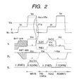
- QR should be conducting at VN(H) and non-conducting at VN(L).
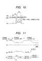
- the data line precharged to VDD either discharges to 0 V as illustrated or holds VDD.
- the write transistor QW non-conducting it is necessary to make the write transistor QW non-conducting to prevent the read operation from being adversely affected by QW.
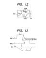
- the condition which makes QW non-conducting at VN(L) should be met because QE has a lower source voltage and more readily becomes conducting at VN(L) than at VN(H).
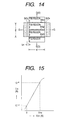
- the signal voltage emerging on the data line becomes extremely high. As stated above, it can be turned into the amplitude of the source voltage depending on the design. Further, the number of memory cells that can be connected to one data line is unlimited as a matter of principle. As there is a gain even if the incidental capacity (CD) of the data line increases, the memory cell will operate properly. As opposed to this, since any known DRAM cell has no gain, the signal voltage emerging on the data line is extremely small.
Landscapes
- Engineering & Computer Science (AREA)
- Microelectronics & Electronic Packaging (AREA)
- Computer Hardware Design (AREA)
- Dram (AREA)
- Read Only Memory (AREA)
- Semiconductor Memories (AREA)
- Non-Volatile Memory (AREA)
Applications Claiming Priority (3)
| Application Number | Priority Date | Filing Date | Title |
|---|---|---|---|
| JP28066398 | 1998-10-02 | ||
| JP10280663A JP2000113683A (ja) | 1998-10-02 | 1998-10-02 | 半導体装置 |
| PCT/JP1999/005338 WO2000021092A1 (fr) | 1998-10-02 | 1999-09-29 | Dispositif a semi-conducteurs |
Publications (1)
| Publication Number | Publication Date |
|---|---|
| EP1120791A1 true EP1120791A1 (de) | 2001-08-01 |
Family
ID=17628208
Family Applications (1)
| Application Number | Title | Priority Date | Filing Date |
|---|---|---|---|
| EP99969937A Withdrawn EP1120791A1 (de) | 1998-10-02 | 1999-09-29 | Halbleiterschaltung |
Country Status (7)
| Country | Link |
|---|---|
| EP (1) | EP1120791A1 (de) |
| JP (1) | JP2000113683A (de) |
| KR (1) | KR20010075543A (de) |
| CN (1) | CN1324486A (de) |
| AU (1) | AU5998699A (de) |
| TW (1) | TW449748B (de) |
| WO (1) | WO2000021092A1 (de) |
Cited By (5)
| Publication number | Priority date | Publication date | Assignee | Title |
|---|---|---|---|---|
| WO2011099389A1 (en) | 2010-02-12 | 2011-08-18 | Semiconductor Energy Laboratory Co., Ltd. | Semiconductor device and driving method of the same |
| EP2428959A1 (de) * | 2010-09-13 | 2012-03-14 | Semiconductor Energy Laboratory Co, Ltd. | Halbleiterbauelement |
| US9825037B2 (en) | 2010-08-06 | 2017-11-21 | Semiconductor Energy Laboratory Co., Ltd. | Semiconductor device and driving method thereof |
| US10236033B2 (en) | 2010-09-14 | 2019-03-19 | Semiconductor Energy Laboratory Co., Ltd. | Memory device and semiconductor device |
| US11923372B2 (en) | 2012-02-29 | 2024-03-05 | Semiconductor Energy Laboratory Co., Ltd. | Semiconductor device |
Families Citing this family (18)
| Publication number | Priority date | Publication date | Assignee | Title |
|---|---|---|---|---|
| JP2000269358A (ja) * | 1999-03-17 | 2000-09-29 | Hitachi Ltd | 半導体装置およびその製造方法 |
| US6570206B1 (en) | 2000-03-29 | 2003-05-27 | Hitachi, Ltd. | Semiconductor device |
| JP2002203913A (ja) | 2000-12-28 | 2002-07-19 | Hitachi Ltd | 半導体記憶装置の製造方法および半導体記憶装置 |
| JP2002245777A (ja) | 2001-02-20 | 2002-08-30 | Hitachi Ltd | 半導体装置 |
| JP2002269976A (ja) * | 2001-03-09 | 2002-09-20 | Hitachi Ltd | 半導体記憶装置 |
| JP2003017591A (ja) * | 2001-07-03 | 2003-01-17 | Hitachi Ltd | 半導体記憶装置 |
| US6677633B2 (en) | 2002-09-24 | 2004-01-13 | Hitachi, Ltd. | Semiconductor device |
| US6831866B1 (en) * | 2003-08-26 | 2004-12-14 | International Business Machines Corporation | Method and apparatus for read bitline clamping for gain cell DRAM devices |
| CN101593560B (zh) * | 2008-05-26 | 2011-07-06 | 中芯国际集成电路制造(北京)有限公司 | 随机存取存储器及其存储单元 |
| WO2011089852A1 (en) | 2010-01-22 | 2011-07-28 | Semiconductor Energy Laboratory Co., Ltd. | Semiconductor memory device and driving method thereof |
| WO2011096262A1 (en) * | 2010-02-05 | 2011-08-11 | Semiconductor Energy Laboratory Co., Ltd. | Semiconductor device |
| CN102754162B (zh) * | 2010-02-19 | 2015-12-09 | 株式会社半导体能源研究所 | 半导体器件及半导体器件的驱动方法 |
| WO2011108475A1 (en) * | 2010-03-04 | 2011-09-09 | Semiconductor Energy Laboratory Co., Ltd. | Semiconductor memory device and semiconductor device |
| JP5923248B2 (ja) * | 2010-05-20 | 2016-05-24 | 株式会社半導体エネルギー研究所 | 半導体装置 |
| US8582348B2 (en) * | 2010-08-06 | 2013-11-12 | Semiconductor Energy Laboratory Co., Ltd. | Semiconductor device and method for driving semiconductor device |
| US8339837B2 (en) * | 2010-08-26 | 2012-12-25 | Semiconductor Energy Laboratory Co., Ltd. | Driving method of semiconductor device |
| US8634228B2 (en) * | 2010-09-02 | 2014-01-21 | Semiconductor Energy Laboratory Co., Ltd. | Driving method of semiconductor device |
| CN109887536A (zh) * | 2019-02-13 | 2019-06-14 | 上海新储集成电路有限公司 | 一种非易失性存储单元结构 |
Family Cites Families (4)
| Publication number | Priority date | Publication date | Assignee | Title |
|---|---|---|---|---|
| JPS634671A (ja) * | 1986-06-25 | 1988-01-09 | Hitachi Ltd | 半導体記憶装置 |
| JPH0254572A (ja) * | 1988-08-18 | 1990-02-23 | Matsushita Electric Ind Co Ltd | 半導体記憶装置 |
| KR100215866B1 (ko) * | 1996-04-12 | 1999-08-16 | 구본준 | 커패시터가 없는 디램 및 그의 제조방법 |
| JP4162280B2 (ja) * | 1996-11-15 | 2008-10-08 | 株式会社日立製作所 | メモリデバイスおよびメモリアレイ回路 |
-
1998
- 1998-10-02 JP JP10280663A patent/JP2000113683A/ja active Pending
-
1999
- 1999-09-29 KR KR1020017004188A patent/KR20010075543A/ko not_active Ceased
- 1999-09-29 EP EP99969937A patent/EP1120791A1/de not_active Withdrawn
- 1999-09-29 AU AU59986/99A patent/AU5998699A/en not_active Abandoned
- 1999-09-29 WO PCT/JP1999/005338 patent/WO2000021092A1/ja not_active Ceased
- 1999-09-29 CN CN99812731A patent/CN1324486A/zh active Pending
- 1999-10-02 TW TW088117019A patent/TW449748B/zh not_active IP Right Cessation
Non-Patent Citations (1)
| Title |
|---|
| See references of WO0021092A1 * |
Cited By (13)
| Publication number | Priority date | Publication date | Assignee | Title |
|---|---|---|---|---|
| EP2534679A4 (de) * | 2010-02-12 | 2016-03-16 | Semiconductor Energy Lab | Halbleiterbauelement und antriebsverfahren dafür |
| WO2011099389A1 (en) | 2010-02-12 | 2011-08-18 | Semiconductor Energy Laboratory Co., Ltd. | Semiconductor device and driving method of the same |
| US9825037B2 (en) | 2010-08-06 | 2017-11-21 | Semiconductor Energy Laboratory Co., Ltd. | Semiconductor device and driving method thereof |
| US10453846B2 (en) | 2010-09-13 | 2019-10-22 | Semiconductor Energy Laboratory Co., Ltd. | Semiconductor device |
| US8767442B2 (en) | 2010-09-13 | 2014-07-01 | Semiconductor Energy Laboratory Co., Ltd. | Semiconductor device including memory cell array |
| EP2428959A1 (de) * | 2010-09-13 | 2012-03-14 | Semiconductor Energy Laboratory Co, Ltd. | Halbleiterbauelement |
| US10236033B2 (en) | 2010-09-14 | 2019-03-19 | Semiconductor Energy Laboratory Co., Ltd. | Memory device and semiconductor device |
| US10665270B2 (en) | 2010-09-14 | 2020-05-26 | Semiconductor Energy Laboratory Co., Ltd. | Memory device comprising stacked memory cell |
| US11568902B2 (en) | 2010-09-14 | 2023-01-31 | Semiconductor Energy Laboratory Co., Ltd. | Semiconductor device including transistors with different channel-formation materials |
| US12040042B2 (en) | 2010-09-14 | 2024-07-16 | Semiconductor Energy Laboratory Co., Ltd. | Semiconductor device including transistor |
| US11923372B2 (en) | 2012-02-29 | 2024-03-05 | Semiconductor Energy Laboratory Co., Ltd. | Semiconductor device |
| US12382723B2 (en) | 2012-02-29 | 2025-08-05 | Semiconductor Energy Laboratory Co., Ltd. | Semiconductor device |
| US12550447B2 (en) | 2012-02-29 | 2026-02-10 | Semiconductor Energy Laboratory Co., Ltd. | Semiconductor device |
Also Published As
| Publication number | Publication date |
|---|---|
| AU5998699A (en) | 2000-04-26 |
| WO2000021092A1 (fr) | 2000-04-13 |
| JP2000113683A (ja) | 2000-04-21 |
| CN1324486A (zh) | 2001-11-28 |
| KR20010075543A (ko) | 2001-08-09 |
| TW449748B (en) | 2001-08-11 |
Similar Documents
| Publication | Publication Date | Title |
|---|---|---|
| EP1120791A1 (de) | Halbleiterschaltung | |
| US6512714B2 (en) | Semiconductor memory device equipped with dummy cells | |
| JP3781270B2 (ja) | 半導体集積回路装置 | |
| EP1475805B1 (de) | Halbleiterspeicheranordnung | |
| US7023721B2 (en) | Semiconductor integrated circuit device | |
| US7145811B2 (en) | Semiconductor storage device | |
| US6787835B2 (en) | Semiconductor memories | |
| US7123509B2 (en) | Floating body cell memory and reading and writing circuit thereof | |
| US20050146928A1 (en) | 3T1D memory cells using gated diodes and methods of use thereof | |
| JPWO2000070682A1 (ja) | 半導体集積回路装置 | |
| US5745423A (en) | Low power precharge circuit for a dynamic random access memory | |
| US7023752B2 (en) | Semiconductor storage apparatus | |
| JPH06326272A (ja) | 半導体記憶装置 | |
| WO1985002314A2 (en) | Semiconductor memory | |
| JP4373464B2 (ja) | 半導体装置 | |
| US5331595A (en) | Semiconductor memory device having IO line pair to be equalized and divided into blocks and operating method thereof | |
| EP0603651B1 (de) | Datenleseschaltung für Speichersystem mit einem dynamischen verstärkten Speicher | |
| JP2002269975A (ja) | 半導体記憶装置 | |
| JPS63894A (ja) | メモリ | |
| HK1003737B (en) | Signal sensing circuits for memory system using dynamic gain memory | |
| JPS62226494A (ja) | メモリ |
Legal Events
| Date | Code | Title | Description |
|---|---|---|---|
| PUAI | Public reference made under article 153(3) epc to a published international application that has entered the european phase |
Free format text: ORIGINAL CODE: 0009012 |
|
| 17P | Request for examination filed |
Effective date: 20010423 |
|
| AK | Designated contracting states |
Kind code of ref document: A1 Designated state(s): AT BE CH CY DE DK ES FI FR GB GR IE IT LI LU MC NL PT SE |
|
| STAA | Information on the status of an ep patent application or granted ep patent |
Free format text: STATUS: THE APPLICATION HAS BEEN WITHDRAWN |
|
| 18W | Application withdrawn |
Withdrawal date: 20020723 |
|
| RBV | Designated contracting states (corrected) |
Designated state(s): DE FR GB IT NL |