EP1120837A2 - Panneau de cellules solaires - Google Patents
Panneau de cellules solaires Download PDFInfo
- Publication number
- EP1120837A2 EP1120837A2 EP01300475A EP01300475A EP1120837A2 EP 1120837 A2 EP1120837 A2 EP 1120837A2 EP 01300475 A EP01300475 A EP 01300475A EP 01300475 A EP01300475 A EP 01300475A EP 1120837 A2 EP1120837 A2 EP 1120837A2
- Authority
- EP
- European Patent Office
- Prior art keywords
- connector
- solar cell
- housing
- cell panel
- terminal
- Prior art date
- Legal status (The legal status is an assumption and is not a legal conclusion. Google has not performed a legal analysis and makes no representation as to the accuracy of the status listed.)
- Granted
Links
Images


Classifications
-
- H—ELECTRICITY
- H02—GENERATION; CONVERSION OR DISTRIBUTION OF ELECTRIC POWER
- H02S—GENERATION OF ELECTRIC POWER BY CONVERSION OF INFRARED RADIATION, VISIBLE LIGHT OR ULTRAVIOLET LIGHT, e.g. USING PHOTOVOLTAIC [PV] MODULES
- H02S40/00—Components or accessories in combination with PV modules, not provided for in groups H02S10/00 - H02S30/00
- H02S40/30—Electrical components
- H02S40/34—Electrical components comprising specially adapted electrical connection means to be structurally associated with the PV module, e.g. junction boxes
-
- H—ELECTRICITY
- H10—SEMICONDUCTOR DEVICES; ELECTRIC SOLID-STATE DEVICES NOT OTHERWISE PROVIDED FOR
- H10F—INORGANIC SEMICONDUCTOR DEVICES SENSITIVE TO INFRARED RADIATION, LIGHT, ELECTROMAGNETIC RADIATION OF SHORTER WAVELENGTH OR CORPUSCULAR RADIATION
- H10F77/00—Constructional details of devices covered by this subclass
- H10F77/93—Interconnections
- H10F77/933—Interconnections for devices having potential barriers
- H10F77/935—Interconnections for devices having potential barriers for photovoltaic devices or modules
- H10F77/937—Busbar structures for modules
-
- H—ELECTRICITY
- H10—SEMICONDUCTOR DEVICES; ELECTRIC SOLID-STATE DEVICES NOT OTHERWISE PROVIDED FOR
- H10F—INORGANIC SEMICONDUCTOR DEVICES SENSITIVE TO INFRARED RADIATION, LIGHT, ELECTROMAGNETIC RADIATION OF SHORTER WAVELENGTH OR CORPUSCULAR RADIATION
- H10F77/00—Constructional details of devices covered by this subclass
- H10F77/93—Interconnections
- H10F77/933—Interconnections for devices having potential barriers
- H10F77/935—Interconnections for devices having potential barriers for photovoltaic devices or modules
- H10F77/939—Output lead wires or elements
-
- Y—GENERAL TAGGING OF NEW TECHNOLOGICAL DEVELOPMENTS; GENERAL TAGGING OF CROSS-SECTIONAL TECHNOLOGIES SPANNING OVER SEVERAL SECTIONS OF THE IPC; TECHNICAL SUBJECTS COVERED BY FORMER USPC CROSS-REFERENCE ART COLLECTIONS [XRACs] AND DIGESTS
- Y02—TECHNOLOGIES OR APPLICATIONS FOR MITIGATION OR ADAPTATION AGAINST CLIMATE CHANGE
- Y02B—CLIMATE CHANGE MITIGATION TECHNOLOGIES RELATED TO BUILDINGS, e.g. HOUSING, HOUSE APPLIANCES OR RELATED END-USER APPLICATIONS
- Y02B10/00—Integration of renewable energy sources in buildings
- Y02B10/10—Photovoltaic [PV]
-
- Y—GENERAL TAGGING OF NEW TECHNOLOGICAL DEVELOPMENTS; GENERAL TAGGING OF CROSS-SECTIONAL TECHNOLOGIES SPANNING OVER SEVERAL SECTIONS OF THE IPC; TECHNICAL SUBJECTS COVERED BY FORMER USPC CROSS-REFERENCE ART COLLECTIONS [XRACs] AND DIGESTS
- Y02—TECHNOLOGIES OR APPLICATIONS FOR MITIGATION OR ADAPTATION AGAINST CLIMATE CHANGE
- Y02E—REDUCTION OF GREENHOUSE GAS [GHG] EMISSIONS, RELATED TO ENERGY GENERATION, TRANSMISSION OR DISTRIBUTION
- Y02E10/00—Energy generation through renewable energy sources
- Y02E10/50—Photovoltaic [PV] energy
-
- Y—GENERAL TAGGING OF NEW TECHNOLOGICAL DEVELOPMENTS; GENERAL TAGGING OF CROSS-SECTIONAL TECHNOLOGIES SPANNING OVER SEVERAL SECTIONS OF THE IPC; TECHNICAL SUBJECTS COVERED BY FORMER USPC CROSS-REFERENCE ART COLLECTIONS [XRACs] AND DIGESTS
- Y10—TECHNICAL SUBJECTS COVERED BY FORMER USPC
- Y10S—TECHNICAL SUBJECTS COVERED BY FORMER USPC CROSS-REFERENCE ART COLLECTIONS [XRACs] AND DIGESTS
- Y10S136/00—Batteries: thermoelectric and photoelectric
- Y10S136/291—Applications
-
- Y—GENERAL TAGGING OF NEW TECHNOLOGICAL DEVELOPMENTS; GENERAL TAGGING OF CROSS-SECTIONAL TECHNOLOGIES SPANNING OVER SEVERAL SECTIONS OF THE IPC; TECHNICAL SUBJECTS COVERED BY FORMER USPC CROSS-REFERENCE ART COLLECTIONS [XRACs] AND DIGESTS
- Y10—TECHNICAL SUBJECTS COVERED BY FORMER USPC
- Y10S—TECHNICAL SUBJECTS COVERED BY FORMER USPC CROSS-REFERENCE ART COLLECTIONS [XRACs] AND DIGESTS
- Y10S136/00—Batteries: thermoelectric and photoelectric
- Y10S136/291—Applications
- Y10S136/293—Circuits
Definitions
- the present invention relates to a solar cell panel for electricity generation using solar energy, having a connector incorporated in it.
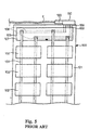
- Fig. 5 shows one form of known solar cell panel 100 having a connector 110 for connecting with an external connector 120 provided on the end of cable K.
- the connector 110 is firmly fixed on the outer periphery of the panel 100 which is made of a pair of glass sheets 101, between which a plurality of solar cell elements 102 in a two-dimensional array are sandwiched.
- the solar cell elements 102 are electrically connected mutually in series or in parallel between the pair of glass sheets 101 by tape-like conductors 103, which are electrically connected with the connector 110 through a connecting sheet 105.
- the connecting sheet 105 a pair of thin ribbon-like conductors 106, which are arranged in parallel at suitable spacing, is sandwiched by insulation sheets 107.
- the conductors 103 from the solar cell elements 102 are electrically connected by soldering, etc. to the respective conductors 106.
- Tape-like conductors 109 are electrically connected by soldering, etc. to the conductors 106 in the end area of the connecting sheet 105, and extend to the outer peripheral area of the panel 100 to be connected to the connector 110.
- the solar cell panel 100 is electrically connected to an external load or storage battery.
- the electrical connection in connector 110 and external connector 120 is performed by locking together of positive and negative terminals inside the connectors.
- a negative and a positive terminal are arranged in the housing of the connector 110, and electrically connected by for example soldering to the conductors 109 which extend from the outer peripheral area of the panel 100.
- space is required for connecting the conductors 109 and the negative terminal and the positive terminal inside the connector 110, which causes a problem that the whole shape of the connector 110 becomes large. This is unfavourable for design reasons, because the connector 110 itself is conspicuous when the solar cell panel is installed on the window frame or on the roof of a building, etc. If a large frame body is installed around the panel 100 to hide the connector 110, the effective area contributing to solar energy electricity generation is decreased.
- US-A-4283106 shows a single-pole connector mountable on a solar panel by engagement of a slot on the connector housing with a cut-out in a peripheral projecting flange of the panel.
- a strip-shape conductor protrudes from between superimposed sheets of the panel and is soldered to an exposed base member of a folded metal terminal construction mounted in the connector housing.
- the arrangement is space-consuming, since both the flange and the connector project above the plane of the panel. Soldering of the conductor to the terminal construction is inconvenient.
- An object of the present invention is to provide a connector of compact structure on a solar cell panel.
- a solar cell panel having a pair of superimposed plates and at least one solar energy cell sandwiched between the plates.
- a connector for use in making electrical connection to an external connection member in use of the solar cell is mounted on the superimposed plates at their periphery.
- At least one one-piece electrical conductor member has a first end located between the superimposed plates and electrically connected to the solar energy cell and a second end which protrudes from the periphery of the plates and is received and held in a housing of the connector where it constitutes an electrical terminal for making electrical connection with the external connection member in use.
- the electrical conductor is of ribbon-like or strip shape.
- This construction permits a compact and simple connector to be provided at the periphery of the panel.
- the one-piece electrical conductor member, or each such electrical member is bent twice, outside the superimposed plates, first to extend in a first direction which is the thickness direction of the superimposed members and secondly to extend in a second direction substantially parallel to the adjacent zone of the periphery of the panel, so as to constitute a pair of parallel spaced terminals of the connector extending in the second direction.
- a bypass diode may easily be incorporated, in the housing of the connector, between the two conductors.
- the housing has locking means for engaging the electrical conductor member and holding it in its longitudinal position in the housing.
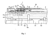
- Figs. 1 to 4 The solar cell panel having a connector which is an embodiment of the present invention is shown in Figs. 1 to 4 in which the solar cell panel 100 itself is the same as in Fig. 5 except for conductor 109 and connector 110, so that repetition of its description is not needed here.
- Figs. 1 to 3 are described as a matter of convenience with reference to a forward direction which is to the right and a backward direction which is to the left (see arrows in Figs. 2 and 3).
- a connector 1 is installed on the outer periphery of panel 100 to be able to be connected with an external connector 50 which is installed at the end of cable K.
- the ends of the conductors 30 which extend out from the outer periphery of the panel 100 are held in an insulating housing 2 of the connector 1 and act as terminals 30b for connecting with terminals 55 inside the external connector 50.
- the external connector 50 is a two terminal connector installed at the end of a two core cable K, having a housing 51 as shown in Fig. 1 containing two connecting terminals 55 arranged spaced apart and aligned and electrically connected with the respective cores of the external cable K.
- Each terminal 55 is in use connected with the respective terminal 30b by forcing the planar terminal 30b between a resilient tongue 57 and a pair of abutment seats 58 (of which one is seen in Fig. 1) of a connecting portion 56 of the terminal 55.
- the whole terminal 55 is formed of cut and bent metal sheet.
- the two abutment seats 58 are formed by side flange parts which are folded over so that their edges project upwardly towards the tongue 57.
- the housing 51 has a portion 60 extending towards its tip side having a hook 60a which engages in a latching manner with a recess 3a of the housing 2 of the connector 1.
- Each one-piece conductor 30 is formed by bending a metal strip member made by punching out thin sheet, and has at one end a connecting area 30a sandwiched together with connecting sheet 105 between a pair of glass sheets 101 of the panel.
- the glass sheets 101 are superimposed with adhesive or filler between them which supports the connecting area 30a of each conductor 30 in the required position between them.
- the connecting areas 30a of the conductors 30 are arranged between the glass sheets 101 aligned at required intervals along the edge of panel 100 and are electrically connected, e.g. by soldering, to the thin ribbon-like conductors 106 in connecting sheet 105, which are connected to the leads 103 of the solar cell elements 102 in the connecting sheet 105.
- the portions of the conductors 30 protruding from the outer periphery of the panel 100 are bent twice, to extend first in the thickness direction of the panel 100 and secondly in the direction parallel to the edge surface of the panel 100, whereby in housing 2 they extend in a coplanar, spaced and aligned manner as the respective terminals 30b.
- the housing 2 has a terminal-supporting region 10 having projections 13a which engage in recesses 30c cut in the terminals 30b, to locate the terminals 30b in the backwards/forward direction.
- the housing 2 of the connector is flat, and of rectangular cross-section as seen in Fig. 4, in which portion 1 of the sheets 101 are shown diagrammatically.
- the housing 1 has a cavity region 15 bounded by the housing wall containing the bent portions of the conductors 30, and having a slit 16 in its base on the panel 100, at a location corresponding to the gap between the pair of glass sheets 101, so that the conductors 30 can extend from between the sheets directly into the cavity 15.
- a diode D for effecting electrical bypass of the panel 100, which is required under certain operating conditions.
- the diode D is connected by leads DL, to the respective conductors 30, e.g. by soldering.
- a sheet-shape closure 19 closes the end opening of the cavity 15 at the rear side of the connector, in order to prevent access of water.
- the housing 2 has a barrier wall 11 with through holes 12, through which pass the respective terminals 30b.
- the terminals 30b are retained in their aligned position parallel to the edge of the panel 100.
- the members 13 have a flat shape, and are elastically deformable in the transverse direction.
- the extremity of each member 13 has a surface 13b inclined to the insertion direction of the terminal 30b, so that the terminal 30b pushes the member 13 aside until the projection 13a is engaged with the recess 30c by the spring back of the member 13.
- the forward portion of the housing 2 has an open ended cavity 7 to receive the housing 51 of the connector 50.
- the rearward part of this cavity 7 is divided by a partition 6a to form a pair of terminal insertion passages 6.
- the terminals 30b extend along these terminal insertion passages 6, and receive and engage the terminals 55 of the external connector 50.
- Support members 20 for the terminals 30b are fully slidable along the respective terminal receiving passages 6, and have through-holes 21 through which the terminals 30b pass.
- the supports 20 serve to maintain the alignment position of the terminals 30b.
- a resilient member, such as a coil spring 25, is provided between the base of each terminal receiving passage 6 and the support 20, to urge the support 20 in the forward direction.
- a stop (not shown) retains the support 20 in the passage 6.
- the housing 2 has a wide groove 3 which receives the extending portion 60 of the housing 51 of the external connector 50, so that the hook end 60a engages with the correspondingly shaped recess 3a, to lock the connectors together.
- the connector 1 may be assembled in advance, and the connecting portions 30a projecting from the slit 16 are inserted and connected to the conductors 106 of the connecting sheet 105, e.g. by soldering, before being sandwiched between the glass sheets 101.
- the housing 2, with its sealing end closure 19, is adhesively bonded to the peripheral edge faces of the sheets 101, so that the cavity 15 is sealed to the sheets 101.
- the arrangement of the bent conductors 30 extending out of the periphery of the panel 100 into the flat connector housing 2 provides a compact shape for the whole construction, as compared with that of Fig. 5. Because the conductor 30 is bent first in the thickness direction of the panel 100 and then in the direction parallel to the periphery of the panel 100, a compact arrangement is achieved, and the external connector 50 is joined to the connector 1 in the direction parallel to the edge of the panel 100.
- the two terminals 30b are coplanar, to make the construction compact. However, within the scope of the invention, the terminals 30b may extend perpendicularly to the edge direction of the panel 100, so that the connection with the external connector 50 is made in this perpendicular direction.
- the connector 1 is located between the planes of the exterior main faces of the panel.
- bypass diode D can be easily incorporated into the solar cell panel construction.
- the return force of the springs 25 ensures continued engagement of the hook 60a with the corresponding recess 3a.
Landscapes
- Photovoltaic Devices (AREA)
- Hybrid Cells (AREA)
Applications Claiming Priority (2)
| Application Number | Priority Date | Filing Date | Title |
|---|---|---|---|
| JP2000013749 | 2000-01-24 | ||
| JP2000013749A JP2001210849A (ja) | 2000-01-24 | 2000-01-24 | 太陽電池パネル用のコネクタ |
Publications (3)
| Publication Number | Publication Date |
|---|---|
| EP1120837A2 true EP1120837A2 (fr) | 2001-08-01 |
| EP1120837A3 EP1120837A3 (fr) | 2004-04-21 |
| EP1120837B1 EP1120837B1 (fr) | 2006-09-13 |
Family
ID=18541297
Family Applications (1)
| Application Number | Title | Priority Date | Filing Date |
|---|---|---|---|
| EP01300475A Expired - Lifetime EP1120837B1 (fr) | 2000-01-24 | 2001-01-19 | Panneau de cellules solaires |
Country Status (4)
| Country | Link |
|---|---|
| US (1) | US6437236B2 (fr) |
| EP (1) | EP1120837B1 (fr) |
| JP (1) | JP2001210849A (fr) |
| DE (1) | DE60122951T2 (fr) |
Cited By (7)
| Publication number | Priority date | Publication date | Assignee | Title |
|---|---|---|---|---|
| WO2005067060A1 (fr) * | 2003-12-24 | 2005-07-21 | Glaswerke Arnold Gmbh & Co. Kg | Vitre d'isolation pour modules photovoltaiques |
| WO2008042194A2 (fr) | 2006-10-03 | 2008-04-10 | Sunpower Corporation | Formation de barres de bus pour module photovoltaïque |
| FR2915345A1 (fr) * | 2007-04-20 | 2008-10-24 | Imphy Alloys Sa | Bati support d'un panneau electriquement actif tel qu'un panneau photovoltaique |
| EP2096681A1 (fr) * | 2008-02-27 | 2009-09-02 | Arcelormittal-Stainless & Nickel | Dispositif de connexion électrique externe des cellules électriquement actives d'un panneau électriquement actif, telles que les cellules génératrices d'électricité d'un panneau photovoltaïque |
| WO2012038124A1 (fr) * | 2010-09-20 | 2012-03-29 | Robert Bosch Gmbh | Ensemble contact de raccordement et ensemble photopile |
| WO2011141203A3 (fr) * | 2010-05-12 | 2012-07-26 | Robert Bosch Gmbh | Système de mise en contact par connexion pour modules solaires |
| WO2016008964A1 (fr) * | 2014-07-17 | 2016-01-21 | Solibro Hi-Tech Gmbh | Module solaire et procédé de production d'un module solaire |
Families Citing this family (37)
| Publication number | Priority date | Publication date | Assignee | Title |
|---|---|---|---|---|
| US8664030B2 (en) | 1999-03-30 | 2014-03-04 | Daniel Luch | Collector grid and interconnect structures for photovoltaic arrays and modules |
| JP2002094101A (ja) * | 2000-09-13 | 2002-03-29 | Sumitomo Wiring Syst Ltd | 太陽電池パネル用の端子ボックス |
| JP3769509B2 (ja) * | 2002-01-31 | 2006-04-26 | 木谷電器株式会社 | 太陽電池モジュール用端子ボックス |
| DE10239845C1 (de) * | 2002-08-29 | 2003-12-24 | Day4 Energy Inc | Elektrode für fotovoltaische Zellen, fotovoltaische Zelle und fotovoltaischer Modul |
| JP4069834B2 (ja) * | 2003-08-20 | 2008-04-02 | 松下電工株式会社 | 太陽光発電システム |
| US7759158B2 (en) * | 2005-03-22 | 2010-07-20 | Applied Materials, Inc. | Scalable photovoltaic cell and solar panel manufacturing with improved wiring |
| DE102005039952A1 (de) * | 2005-08-24 | 2007-03-08 | Siegfried Renn | Photovoltaisches Solarmodul |
| US20070193618A1 (en) * | 2005-09-19 | 2007-08-23 | Solar Roofing Systems, Inc. | Integrated Solar Roofing System |
| US8227688B1 (en) | 2005-10-17 | 2012-07-24 | Solaria Corporation | Method and resulting structure for assembling photovoltaic regions onto lead frame members for integration on concentrating elements for solar cells |
| US7910822B1 (en) | 2005-10-17 | 2011-03-22 | Solaria Corporation | Fabrication process for photovoltaic cell |
| US20070144577A1 (en) * | 2005-12-23 | 2007-06-28 | Rubin George L | Solar cell with physically separated distributed electrical contacts |
| US9236512B2 (en) | 2006-04-13 | 2016-01-12 | Daniel Luch | Collector grid and interconnect structures for photovoltaic arrays and modules |
| US9006563B2 (en) | 2006-04-13 | 2015-04-14 | Solannex, Inc. | Collector grid and interconnect structures for photovoltaic arrays and modules |
| US9865758B2 (en) | 2006-04-13 | 2018-01-09 | Daniel Luch | Collector grid and interconnect structures for photovoltaic arrays and modules |
| US8729385B2 (en) | 2006-04-13 | 2014-05-20 | Daniel Luch | Collector grid and interconnect structures for photovoltaic arrays and modules |
| US8884155B2 (en) | 2006-04-13 | 2014-11-11 | Daniel Luch | Collector grid and interconnect structures for photovoltaic arrays and modules |
| US8822810B2 (en) | 2006-04-13 | 2014-09-02 | Daniel Luch | Collector grid and interconnect structures for photovoltaic arrays and modules |
| US7700878B2 (en) * | 2006-08-31 | 2010-04-20 | Antaya Technologies Corporation | Buss bar strip |
| US20080092944A1 (en) * | 2006-10-16 | 2008-04-24 | Leonid Rubin | Semiconductor structure and process for forming ohmic connections to a semiconductor structure |
| JP4989268B2 (ja) * | 2007-03-23 | 2012-08-01 | 三洋電機株式会社 | 太陽電池モジュール |
| US7910392B2 (en) | 2007-04-02 | 2011-03-22 | Solaria Corporation | Method and system for assembling a solar cell package |
| US20090056806A1 (en) * | 2007-09-05 | 2009-03-05 | Solaria Corporation | Solar cell structure including a plurality of concentrator elements with a notch design and predetermined radii and method |
| ES2370863T3 (es) * | 2007-04-13 | 2011-12-23 | Huber+Suhner Ag | Caja de conexión |
| US20080290368A1 (en) * | 2007-05-21 | 2008-11-27 | Day4 Energy, Inc. | Photovoltaic cell with shallow emitter |
| US8119902B2 (en) | 2007-05-21 | 2012-02-21 | Solaria Corporation | Concentrating module and method of manufacture for photovoltaic strips |
| US7419377B1 (en) * | 2007-08-20 | 2008-09-02 | Solaria Corporation | Electrical coupling device and method for solar cells |
| US7910035B2 (en) | 2007-12-12 | 2011-03-22 | Solaria Corporation | Method and system for manufacturing integrated molded concentrator photovoltaic device |
| KR20100097219A (ko) * | 2007-12-18 | 2010-09-02 | 데이4 에너지 인코포레이티드 | Pv 스트링으로 에지 액세스를 수행하는 광전지 모듈, 연결 방법, 장치, 및 시스템 |
| CN101926009B (zh) * | 2008-01-25 | 2012-01-25 | 应用材料股份有限公司 | 自动化太阳能电池电连接设备 |
| US8293568B2 (en) * | 2008-07-28 | 2012-10-23 | Day4 Energy Inc. | Crystalline silicon PV cell with selective emitter produced with low temperature precision etch back and passivation process |
| DE202008011461U1 (de) * | 2008-08-28 | 2010-01-07 | Aleo Solar Ag | Elektrische Solarzellenverbindungen sowie photovoltaische Solarmodule |
| US7850476B2 (en) * | 2008-10-29 | 2010-12-14 | Tyco Electronics Corporation | Low profile solar laminate connector assembly |
| DE102009039370B4 (de) * | 2009-05-20 | 2013-12-05 | Gp Solar Gmbh | Solarzellenmodul mit zumindest einer Laminatfolie, einer weiteren Laminatfolie und einem Querverbinder sowie Verfahren zur Verschaltung von Solarzellen in einem Solarzellenmodul |
| DE102009060604A1 (de) * | 2009-12-23 | 2011-06-30 | Energetica Holding Gmbh | Solar-Modul mit einer Leiterplatte und Verfahren zur Herstellung und Anwendung |
| CN103391722A (zh) | 2010-12-30 | 2013-11-13 | Wm.雷格利Jr.公司 | 糖含量减少的硬糖 |
| JP5594902B2 (ja) * | 2011-04-18 | 2014-09-24 | モレックス インコーポレイテド | 太陽電池パネル用コネクタ及び太陽電池パネル連結体 |
| USD699176S1 (en) | 2011-06-02 | 2014-02-11 | Solaria Corporation | Fastener for solar modules |
Family Cites Families (6)
| Publication number | Priority date | Publication date | Assignee | Title |
|---|---|---|---|---|
| US4310211A (en) * | 1979-12-26 | 1982-01-12 | Amp Incorporated | High current contact system for solar modules |
| US4283106A (en) * | 1980-02-01 | 1981-08-11 | Amp Incorporated | Symmetrical connector for solar panel arrays |
| DE19712747A1 (de) * | 1997-03-26 | 1998-11-05 | Pilkington Solar Int Gmbh | Photovoltaisches Solarmodul in Plattenform |
| JP3359531B2 (ja) * | 1997-03-27 | 2002-12-24 | シャープ株式会社 | 太陽電池モジュール接続構造および太陽電池モジュールの接地方法 |
| JP3478524B2 (ja) * | 1997-07-22 | 2003-12-15 | フィグラ株式会社 | 複層ガラス |
| JP3679611B2 (ja) * | 1998-06-05 | 2005-08-03 | 三洋電機株式会社 | 太陽電池モジュール |
-
2000
- 2000-01-24 JP JP2000013749A patent/JP2001210849A/ja active Pending
-
2001
- 2001-01-19 DE DE60122951T patent/DE60122951T2/de not_active Expired - Fee Related
- 2001-01-19 EP EP01300475A patent/EP1120837B1/fr not_active Expired - Lifetime
- 2001-01-24 US US09/767,861 patent/US6437236B2/en not_active Expired - Fee Related
Cited By (19)
| Publication number | Priority date | Publication date | Assignee | Title |
|---|---|---|---|---|
| WO2005067060A1 (fr) * | 2003-12-24 | 2005-07-21 | Glaswerke Arnold Gmbh & Co. Kg | Vitre d'isolation pour modules photovoltaiques |
| WO2008042194A2 (fr) | 2006-10-03 | 2008-04-10 | Sunpower Corporation | Formation de barres de bus pour module photovoltaïque |
| US10777691B2 (en) | 2006-10-03 | 2020-09-15 | Sunpower Corporation | Formed photovoltaic module busbars |
| US10121910B2 (en) | 2006-10-03 | 2018-11-06 | Sunpower Corporation | Formed photovoltaic module busbars |
| EP3136448A1 (fr) * | 2006-10-03 | 2017-03-01 | Sunpower Corporation | Barres omnibus photovoltaïques formees |
| EP2082433B1 (fr) * | 2006-10-03 | 2016-11-09 | Sunpower Corporation | Formation de barres de bus pour module photovoltaïque |
| US8516755B2 (en) | 2007-04-20 | 2013-08-27 | Aperam Alloys Imphy | Bearing frame for an electrically active panel such as photovoltaic panel |
| FR2915345A1 (fr) * | 2007-04-20 | 2008-10-24 | Imphy Alloys Sa | Bati support d'un panneau electriquement actif tel qu'un panneau photovoltaique |
| WO2008145898A3 (fr) * | 2007-04-20 | 2009-03-19 | Arcelormittal Stainless And Ni | Bâti support d'un panneau électriquement actif tel qu'un panneau photovoltaïque |
| EA016066B1 (ru) * | 2007-04-20 | 2012-01-30 | Арселормитталь-Стейнлесс Энд Никель Эллойз | Опорный каркас электрически активной панели, такой как фотоэлектрическая панель |
| US8286393B2 (en) | 2007-04-20 | 2012-10-16 | Arcelormittal—Stainless and Nickel Alloys | Bearing frame for an electrically active panel such as a photovoltaic panel |
| US8714998B2 (en) | 2008-02-27 | 2014-05-06 | Arcelormittal-Stainless And Nickel Alloys | Device for the external electrical connection of electrically active cells of an electrically active panel |
| CN102007605B (zh) * | 2008-02-27 | 2013-01-02 | 安赛乐米塔尔-不锈钢及镍合金有限公司 | 用于诸如光电面板的发电单元的电活性面板的电活性单元的外部电连接的设备 |
| EA019620B1 (ru) * | 2008-02-27 | 2014-05-30 | Арселормитталь-Стейнлесс Энд Никель Эллойз | Устройство внешнего электрического соединения электрически активных элементов электрически активной панели, таких как электрогенерирующие элементы фотоэлектрической панели |
| WO2009112762A3 (fr) * | 2008-02-27 | 2010-08-26 | Arcelormittal - Stainless And Nickel Alloys | Dispositif de connexion électrique externe des cellules électriquement actives d'un panneau électriquement actif, telles que les cellules génératrices d'électricité d'un panneau photovoltaïque |
| EP2096681A1 (fr) * | 2008-02-27 | 2009-09-02 | Arcelormittal-Stainless & Nickel | Dispositif de connexion électrique externe des cellules électriquement actives d'un panneau électriquement actif, telles que les cellules génératrices d'électricité d'un panneau photovoltaïque |
| WO2011141203A3 (fr) * | 2010-05-12 | 2012-07-26 | Robert Bosch Gmbh | Système de mise en contact par connexion pour modules solaires |
| WO2012038124A1 (fr) * | 2010-09-20 | 2012-03-29 | Robert Bosch Gmbh | Ensemble contact de raccordement et ensemble photopile |
| WO2016008964A1 (fr) * | 2014-07-17 | 2016-01-21 | Solibro Hi-Tech Gmbh | Module solaire et procédé de production d'un module solaire |
Also Published As
| Publication number | Publication date |
|---|---|
| DE60122951T2 (de) | 2007-05-24 |
| EP1120837A3 (fr) | 2004-04-21 |
| US20010009159A1 (en) | 2001-07-26 |
| JP2001210849A (ja) | 2001-08-03 |
| DE60122951D1 (de) | 2006-10-26 |
| EP1120837B1 (fr) | 2006-09-13 |
| US6437236B2 (en) | 2002-08-20 |
Similar Documents
| Publication | Publication Date | Title |
|---|---|---|
| EP1120837A2 (fr) | Panneau de cellules solaires | |
| JP2903918B2 (ja) | ジョイントコネクタ | |
| US7883362B2 (en) | Joint connector, joint terminal and a wiring harness with a joint connector | |
| US6004158A (en) | Electrical connector with secondary locking plates | |
| EP1979968B1 (fr) | Connecteur détecteur de tension pour pile à combustible, et pile à combustible | |
| GB2218576A (en) | Floatingly mounting an electrical connector in a panel | |
| JP2001135378A (ja) | 平形導体の端末構造 | |
| JP3133921B2 (ja) | コネクタ | |
| JP2000208200A (ja) | 防水コネクタ | |
| JP2910623B2 (ja) | ジョイントコネクタ、端子金具及びコネクタハウジング | |
| JP2852497B2 (ja) | 電気コネクタ | |
| CN219303987U (zh) | 一种便于安装软排线的线对板连接器结构 | |
| EP1215761B1 (fr) | Dispositif de connection électrique pour connecter des circuits flexibles plats | |
| US6537080B2 (en) | Joint connector | |
| US20220337188A1 (en) | Modular solar panel design for improved durability & repairability | |
| CN219018768U (zh) | 一种条形光伏接线盒 | |
| US20050059299A1 (en) | Memory card connector | |
| CN113168970B (zh) | 连接模块 | |
| US20240339778A1 (en) | Connector | |
| JP2001028282A (ja) | フラットケーブル用コネクタ | |
| CN223681417U (zh) | 拼装式电磁屏蔽板及使用其的屏蔽门体 | |
| CN222507799U (zh) | 电池盖板、电池及电池包 | |
| JPH10334977A (ja) | コネクタ | |
| JPH0616430Y2 (ja) | 中継端子 | |
| CN103165713B (zh) | 端子盒 |
Legal Events
| Date | Code | Title | Description |
|---|---|---|---|
| PUAI | Public reference made under article 153(3) epc to a published international application that has entered the european phase |
Free format text: ORIGINAL CODE: 0009012 |
|
| 17P | Request for examination filed |
Effective date: 20010208 |
|
| AK | Designated contracting states |
Kind code of ref document: A2 Designated state(s): AT BE CH CY DE DK ES FI FR GB GR IE IT LI LU MC NL PT SE TR |
|
| AX | Request for extension of the european patent |
Free format text: AL;LT;LV;MK;RO;SI |
|
| PUAL | Search report despatched |
Free format text: ORIGINAL CODE: 0009013 |
|
| AK | Designated contracting states |
Kind code of ref document: A3 Designated state(s): AT BE CH CY DE DK ES FI FR GB GR IE IT LI LU MC NL PT SE TR |
|
| AX | Request for extension of the european patent |
Extension state: AL LT LV MK RO SI |
|
| RIC1 | Information provided on ipc code assigned before grant |
Ipc: 7H 01L 31/048 A Ipc: 7H 01L 31/042 B |
|
| 17Q | First examination report despatched |
Effective date: 20040902 |
|
| AKX | Designation fees paid |
Designated state(s): DE |
|
| GRAP | Despatch of communication of intention to grant a patent |
Free format text: ORIGINAL CODE: EPIDOSNIGR1 |
|
| GRAS | Grant fee paid |
Free format text: ORIGINAL CODE: EPIDOSNIGR3 |
|
| GRAA | (expected) grant |
Free format text: ORIGINAL CODE: 0009210 |
|
| AK | Designated contracting states |
Kind code of ref document: B1 Designated state(s): DE |
|
| REF | Corresponds to: |
Ref document number: 60122951 Country of ref document: DE Date of ref document: 20061026 Kind code of ref document: P |
|
| PLBE | No opposition filed within time limit |
Free format text: ORIGINAL CODE: 0009261 |
|
| STAA | Information on the status of an ep patent application or granted ep patent |
Free format text: STATUS: NO OPPOSITION FILED WITHIN TIME LIMIT |
|
| 26N | No opposition filed |
Effective date: 20070614 |
|
| PGFP | Annual fee paid to national office [announced via postgrant information from national office to epo] |
Ref country code: DE Payment date: 20090115 Year of fee payment: 9 |
|
| PG25 | Lapsed in a contracting state [announced via postgrant information from national office to epo] |
Ref country code: DE Free format text: LAPSE BECAUSE OF NON-PAYMENT OF DUE FEES Effective date: 20100803 |